FIELD OF TECHNOLOGY
The present invention relates to a plating structure and a method of
producing the plating structure.
BACKGROUND OF TECHNOLOGY
A fine carbon fiber (diameter: 200 nm or less, aspect ratio: 10 or
more) called "carbon nano tube (CNT)" or "carbon nano fiber" is
characterized by a basic skeleton of carbon (six-ring) arranged in an axial
direction, and it will be used in broad fields of technology due to its high
heat conductivity, high electric conductivity, high slidablity, high
mechanical strength, etc., which are derived form said characteristic.
Various methods of producing the CNT has been known, but the
most advantageous method for mass production is a vapor growth method
(see "Carbon Nano Tube (January 30, 2001)" authored by Kazuyoshi
Tanaka, published by Kagaku Doujin Shuppan Co. Ltd., page 67-77).
For example, the fine carbon fibers are incorporated in a metal to
form a composite material, which can be used for sliding parts, heat
radiators, etc..
Conventionally, the composite material is produced by the steps of:
adding fine carbon fibers into a molten metal; and agitating the molten
metal to mix.
However, in the conventional method, it is very difficult to
uniformly disperse the fine carbon fibers in the molten metal because
specific gravity of the fine carbon fiber is widely different from that of
the molten metal.
Further, heat load is great with respect to the fine carbon fibers and
other substances, so some components cannot be mixed with the fine
carbon fibers.
Thus, the present invention has been invented to solve the above
described problems, and an object of the present invention is to provide a
plating structure, in which fine carbon fibers or derivatives thereof can be
incorporated in a metal at room temperature, and a method of producing
the plating structure.
DISCLOSURE OF THE INVENTION
The plating structure of the present invention comprises a plating
film, in which fine carbon fibers or derivatives thereof are incorporated.
The derivatives include substances prepared by subjecting the fine carbon
fibers to various chemical modifications and by fluorinating the fine
carbon fibers. Note that, the fine carbon fiber means a carbon fiber having
a diameter of about 200 nm or less and an aspect ratio of about 10 or
more.
The incorporation can be performed in a plating step, they can be
incorporated at room temperature, so that heat load of the substances to
be incorporated can be reduced.
In the plating structure, the plating film may be made of a single
metal, or a metal alloy.
In the plating structure, fine resin materials, which are formed into
powders, fibers, etc., may be incorporated.
In the plating structure, the plating film may be formed by
electrolytic plating or electroless plating.
In the plating structure, ends of the fine carbon fibers may project
from a surface of the plating film. The plating structure can be used as an
emitter for field emission.
In the plating structure, the derivatives may be fluorinated carbon
fibers.
An electronic part may comprise cable patterns having the plating
structure.
A mechanical part, e.g., fine gear, may have the plating structure.
A multilayer body may comprise: some plated layers having the
plating structures; and other plated layers being plated with a different
metal. With this structure, heat conductivity in a direction of piling the
layers is different from that in an orthogonal direction (a direction parallel
to each layer), so that the multilayered body can be used as an anisotropic
heat conductor.
A heat radiator may comprise: a plurality of plated layers having
the plating structures; and a plurality of plated layers being plated with a
different metal, wherein two types of the plated layers are alternately
layered, and edges of the plated layers plated with the different metal are
removed by etching whereby a plurality of the plated layers having the
plating structures are arranged parallel with separations.
The method of the present invention comprises the steps of: adding
a dispersing agent and fine carbon fibers or derivatives thereof into a
plating solution so as to disperse the fine carbon fibers or the derivatives
in the plating solution; and plating a substrate in the plating solution so as
to form a plating film, in which the fine carbon fibers or the derivatives
are incorporated, on a surface of the substrate.
In the method, resin materials may be further dispersed in the
plating solution so as to form a plating film, in which the resin materials
and the fine carbon fibers or the derivatives are incorporated, on the
surface of the substrate.
In the method, a cationic and/or nonionic surface acting agent
(surfactant) may be used as the dispersing agent.
In the method, the dispersing agent may be polycarboxylic acid,
e.g., polyacrylic acid, or salt thereof.
The plating solution may include a dispersing agent, which is
polycarboxylic acid, e.g., polyacrylic acid, or salt thereof, so as to
disperse fine carbon fibers therein.
BRIEF DESCRIPTION OF THE DRAWINGS
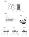
Fig. 1 is an explanation view showing a principle of dispersing
electroplating;
Fig. 2 is an explanation view of CNTs, whose ends project;
Fig. 3 is an explanation view of a photoresist pattern;
Fig. 4 is an explanation view of a state, in which a plating structure
is formed in a concave section;
Fig. 5 is an explanation view of a state, in which the photoresist
pattern is removed;
Fig. 6 is an explanation view of fine gears;
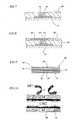
Fig. 7 is an explanation view of a state, in which a via is formed;
Fig. 8 is an explanation view of a multilayered cable patterns;
Fig. 9 is an explanation view of heat radiating fins;
Fig. 10 is an explanation view of a carbon fiber incorporated in a
plating film;
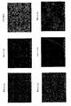
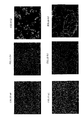
Fig. 11(a) is a micrograph of a surface of a plating film, which is
formed by electrolytic plating in an agitated Base Solution 1 with current
density of 2A/dm2, taken by a scanning electron microscope (SEM); Fig.
11(a') is an enlarged view thereof; Fig. 11(b) is a micrograph of a surface
of a plating film, which is formed by electrolytic plating in a plating
solution of Example 1 with current density of 2A/dm2, taken by the
scanning electron microscope (SEM); Fig. 11(b') is an enlarged view
thereof; Fig. 11(c) is a micrograph of a surface of a plating film, which is
formed by electrolytic plating in a plating solution of Example 2 with
current density of 2A/dm2, taken by the scanning electron microscope
(SEM); Fig. 11(c') is an enlarged view thereof;
Figs. 12(a) and (b) are enlarged views of Fig. 11(c'), whose rate of
enlargement are different;
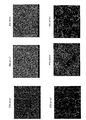
Fig. 13(a) is a micrograph of a surface of a plating film, which is
formed by electrolytic plating in the agitated Base Solution 1 with current
density of 5A/dm2, taken by the scanning electron microscope (SEM); Fig.
13(a') is an enlarged view thereof; Fig. 13(b) is a micrograph of a surface
of a plating film, which is formed by electrolytic plating in the plating
solution of Example 1 with current density of 5A/dm2, taken by the
scanning electron microscope (SEM); Fig. 13(b') is an enlarged view
thereof; Fig. 13(c) is a micrograph of a surface of a plating film, which is
formed by electrolytic plating in plating the solution of Example 2 with
current density of 5A/dm2, taken by the scanning electron microscope
(SEM); Fig. 13(c') is an enlarged view thereof;
Figs. 14(a) and (b) are enlarged views of Fig. 13(c'), whose rate of
enlargement are different;
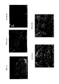
Fig. 15(a) is a micrograph of a surface of a plating film, which is
formed by electrolytic plating in the agitated Base Solution 1 with current
density of 2A/dm2, taken by the scanning electron microscope (SEM); Fig.
15(a') is an enlarged view thereof; Fig. 15(b) is a micrograph of a surface
of a plating film, which is formed by electrolytic plating in a plating
solution of Example 3 with current density of 2A/dm2, taken by the
scanning electron microscope (SEM); Fig. 15(b') is an enlarged view
thereof; Fig. 15(c) is a micrograph of a surface of a plating film, which is
formed by electrolytic plating in a plating solution of Example 4 with
current density of 2A/dm2, taken by the scanning electron microscope
(SEM); Fig. 15(c') is an enlarged view thereof;
Figs. 16(a) and (b) are enlarged views of Fig. 15(c'), whose rate of
enlargement are different;
Fig. 17(a) is a micrograph of a surface of a plating film, which is
formed by electrolytic plating in an agitated Base Solution 2 with current
density of 2A/dm2, taken by the scanning electron microscope (SEM); Fig.
17(a') is an enlarged view thereof; Fig. 17(b) is a micrograph of a surface
of a plating film, which is formed by electrolytic plating in a plating
solution of Example 5 with current density of 2A/dm2, taken by the
scanning electron microscope (SEM); Fig. 17(b') is an enlarged view
thereof; Fig. 17(c) is a micrograph of a surface of a plating film, which is
formed by electrolytic plating in a plating solution of Example 6 with
current density of 2A/dm2, taken by the scanning electron microscope
(SEM); Fig. 17(c') is an enlarged view thereof;
Fig. 18(a) is a micrograph of a surface of a plating film, which is
formed by electrolytic plating in the agitated Base Solution 2 with current
density of 5A/dm2, taken by the scanning electron microscope (SEM); Fig.
18(a') is an enlarged view thereof; Fig. 18(b) is a micrograph of a surface
of a plating film, which is formed by electrolytic plating in the plating
solution of Example 5 with current density of 5A/dm2, taken by the
scanning electron microscope (SEM); Fig. 18(b') is an enlarged view
thereof; Fig. 18(c) is a micrograph of a surface of a plating film, which is
formed by electrolytic plating in the plating solution of Example 6 with
current density of 5A/dm2, taken by the scanning electron microscope
(SEM); Fig. 18(c') is an enlarged view thereof;
Figs. 19 is an enlarged view of Fig. 18(c');
Fig. 20(a) is a micrograph of a surface of a plating film, which is
formed by electrolytic plating in the agitated Base Solution 2 with current
density of 2A/dm2, taken by the scanning electron microscope (SEM); Fig.
20(a') is an enlarged view thereof; Fig. 20(b) is a micrograph of a surface
of a plating film, which is formed by electrolytic plating in a plating
solution of Example 7 with current density of 2A/dm2, taken by the
scanning electron microscope (SEM); Fig. 20(b') is an enlarged view
thereof; Fig. 20(c) is a micrograph of a surface of a plating film, which is
formed by electrolytic plating in a plating solution of Example 8 with
current density of 2A/dm2, taken by the scanning electron microscope
(SEM); Fig. 20(c') is an enlarged view thereof;
Fig. 21 (a) is a micrograph of a surface of a plating film, which is
formed by electrolytic plating in the agitated Base Solution 2 with current
density of 5A/dm2, taken by the scanning electron microscope (SEM); Fig.
21(a') is an enlarged view thereof; Fig. 21(b) is a micrograph of a surface
of a plating film, which is formed by electrolytic plating in the plating
solution of Example 7 with current density of 5A/dm2, taken by the
scanning electron microscope (SEM); Fig. 21(b') is an enlarged view
thereof; Fig. 21(c) is a micrograph of a surface of a plating film, which is
formed by electrolytic plating in the plating solution of Example 8 with
current density of 5A/dm2, taken by the scanning electron microscope
(SEM); Fig. 21(c') is an enlarged view thereof;
Figs. 22(a) and (b) are enlarged views of Fig. 21(c'), whose rate of
enlargement are different; and
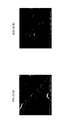
Fig. 23 are micrographs of surfaces of plating films (a: surfaces of
fine carbon fibers are not plated; b: surfaces of fine carbon fibers are
plated by electroless plating in a solution of Example 9) taken by the
scanning electron microscope (SEM).
PREFERRED EMBODIMENTS OF THE INVENTION
Preferred embodiments of the present invention will now be
described in detail with reference to the accompanying drawings.
In the present invention, a dispersing agent and fine carbon fibers
or derivatives of the fine carbon fibers are added in a plating solution so
as to disperse the fine carbon fibers or the derivatives thereof in the
plating solution, then plating is performed so that a plating film, in which
the fine carbon fibers or the derivatives thereof (hereinafter referred to as
"fine carbon fibers, etc." or merely referred to as "fine carbon fibers") are
incorporated in a plating metal, can be formed on a surface of a substrate.
Fig. 1 is a schematic explanation view showing a principle of
dispersing electroplating.
Fine carbon fibers 10, e.g., CNTs, or derivatives of fine carbon
fibers are uniformly dispersed in a plating solution by a dispersing agent.
Preferably, the plating solution is agitated during the plating process, so
that the fine carbon fibers 10, etc. are capable of swimming in the plating
solution without settling down.
In this state, when the plating metal deposits onto a surface of a
substrate 12, the fine carbon fibers 10, etc., which locate on the surface of
the substrate 12, are incorporated in a plating film 14 by electrolytic
plating, so that a composite material (plating structure) of the metal and
the fine carbon fibers, etc. is formed on the surface of the substrate 12.
Note that, the plating method is not limited to a direct current
plating method, further a current inversion plating method, a pulse plating
method, etc. may be employed.
The fine carbon fibers 10 has slight water repellency, and they are
hard to be dispersed in the plating solution without the dispersing agent.
Especially, fluorinated carbon fibers are very hard to be dispersed.
Thus, the dispersing agent is added to the plating solution so as to
disperse the fine carbon fibers, etc. therein.
The dispersing agent is not limited, but cationic or nonionic surface
acting agents (surfactant) can be used as preferred dispersing agents for
electrolytic plating.
Preferred cationic surface acting agents are, for example,
cetyltrimethylammonium chloride, cetyltrimethylammonium bromide,
cetylpyridinium chloride.
To disperse fluorinated carbon fibers, cationic surface acting agents,
e.g., N-[(3-perfluorooctanesulfonamide)
propyl]-N,N,N,-trimethylammonium iodide, may be used.
Preferred anionic surface acting agents are, for example, sodium
dedocyl sulfate, dodecanoic sodium, sodium tetradecylsulfate, fatty acid
sodium, fatty triethanolamine salt, sodium alkylbenzenesulfate, sodium
monoalkyl phosphate.
To disperse fluorinated carbon fibers, anionic surface acting agents,
e.g., perfluorooctane sulfonic acid, perfluorooctane sulfonate,
N-propyl-N-perfluorooctylsulfonyl glycine potassium salt,
bis[2-(N-propyl perfluorooctylsulfonylamino)ethyl] ammonium
phosphate, perfluorocaprylic acid, perfluorooctanoate ammonium, may be
used.
Preferred nonionic surface acting agents are, for example,
polyacrylic acid, polyethylene glycol, polyoxyethylene nonylphenyl ether,
polyoxythylene dodecyl ether, polyoxyethylene lauryl ether,
polyoxyethylene lauryl ether, polyoxyethylene fatty acidic ether,
polyoxyethylene polyoxypropylene block polymer, polyoxyethylene
alkylamine, alkylpolyglucoside, glycerin fatty acidic ester, sorbitan fatty
acidic ester, saccharate fatty acidic ester, propylene glycol fatty acidic
ester.
To disperse fluorinated carbon fibers, nonionic surface acting agents, e.g.,
N-Propyl-N-(2-hydroethyl) perfuorooctane sulfonate amide,
N-polyoxyethylene-N-propylperfluorooctanesulfonate amide,
N-(2-hydoroxyethylene)-N- perfluorooctylsulfonyl benzylamine, may be
used.
The surface acting agents may be solely used or combined.
Further, polycarboxylic acid, e.g., polyacrylic acid, and salt thereof
are suitable dispersing agents. Polyacrylic acid having molecular weight
of about 3000-4000 has high uniform dispersibility.
The plating solution is not limited, but nickel plating solution and
copper plating solution are suitable solutions.
Further, various alloy solutions may be used.
Plating may be performed by not only electrolytic plating but also
electroless plating.
In the case of electroless plating too, when the plating metal
deposits onto the surface of the substrate (plate) 12, the fine carbon fibers,
etc. are incorporated in the plating film 14 as shown in Fig. 1.
Since the fine carbon fibers have high heat conductivity and high
electric conductivity, the plating structures produced by above described
methods also have high heat conductivity and high electric conductivity.
Therefore, they may be widely used, e.g., heat sinks, electric elements.
As shown in Fig. 2, the fine carbon fibers 10 are fixed in the plating
film 14, and their ends project from a surface of the plating film 14.
Especially, the state shown in Fig. 2 is remarkable in the plating film 14
plated with copper.
The plating structure, in which the fine carbon fibers 10 are fixed in
the plating film 14 and their ends project therefrom as shown in Fig. 2, is
suitably used as an emitter for field emission.
Field emission from carbon nano tubes (CNTs) has been studied,
and we pay attention to carbon nano tubes as a material of a display.
To realize the field emission, a strong electric field must be
produced. Thus, the ends must be sharpened as a material of the emitter.
In this regard, CNTs have the great aspect ratio and the sharp ends, and
they are chemically stable,mechanically tough and highly stable at high
temperature, namely they are suitable materials of the emitter for field
emission.
Conventionally, CNTs have been used for a broad cold cathode of a
light emitting device, in which a plurality of CNTs are fixed on a
substrate and headed in the same direction by screen printing, etc..
However, it is difficult to fix a plurality of CNTs on the substrate
with heading in the same direction by screen printing. On the other hand,
in the plating method of the present embodiment, fine carbon fibers
(CNTs) are vertically fixed in the plating film; therefore, the emitter for
field emission, which has a plurality of emitting ends, can be easily
produced.
Figs. 3-5 show steps of producing a fine mechanical part.
In Fig. 3, a resist pattern 16 having a concave section 17 is formed
on the substrate 12 by photolithography. Next, as shown in Fig. 4, a
plating structure 18, in which the fine carbon fibers 10 are incorporated,
is formed in the concave section 17, then the resist pattern 16 is removed
as shown in Fig. 5, so that the pillar-shaped plating structure 18 is
produced on the substrate 12. Next, the plating structure 18 is removed
from the substrate 12, so that fine mechanical parts, e.g., very fine gears
20 shown in Fig. 6, can be produced. Since the plating structure 18 (20)
includes the fine carbon fibers, it can be used as, for example, a pillar
shaped part having high toughness and high durability.
Figs. 7 and 8 show steps of producing a multilayer circuit board,
which is an example of electronic parts.
In Fig. 7, an insulating layer 22 is formed on a cable pattern 21 of a
lower layer by, for example, applying insulating resin; next, a via hole 23,
in which the cable pattern 21 is exposed, is formed in the insulating layer
22 by, for example, laser means; and a plating structure (via) 24, in which
fine carbon fibers are incorporated, is formed in the via hole 23 by the
above described plating method.
In Fig. 8, a resist pattern 25, in which the via 24 is exposed, is
formed on the insulating layer 22 by photolithography, then a cable
pattern 26, which is a plating structure including fine carbon fibers and
which is electrically connected to the via 24, is formed by electroless
plating and electrolytic plating (an additive method). By the above
described steps, the multilayer circuit board, which has the cable patterns
constituted by the plating structures including the fine carbon fibers, can
be produced.
The cable pattern 26, which includes the fine carbon fibers, also
has high electric conductivity.
Note that, the plating method is not limited to the additive method;
for example, the plating film (the plating structure) may be entirely
formed on the insulating layer by electroless plating and electrolytic
plating, then the plating film may be etched so as to form the cable
pattern (a subtractive method).
Note that, another embodiment, not shown, is a cable pattern
connected to electrodes of a semiconductor chip, and the cable pattern
may be produced by forming a polyimide resin layer (an insulating layer)
on the semiconductor chip and forming the plating structure, which
includes fine carbon fibers, thereon as the cable pattern. Bumps for
connecting to an external circuit may be provided to proper positions so
as to relocate the electrodes of the semiconductor chip.
The cable pattern for relocating the electrodes has not only high
electric conductivity but also high heat conductivity; the cable pattern
acts as a heat sink of the semiconductor chip, and heat radiation rate
thereof can be improved.
Fig. 9 shows a heat radiator constituted by the plating structure.
Firstly, a plurality of plated layers 31, each of which is constituted
by the plating structure including the fine carbon fibers (e.g., copper layer
including CNTs), and a plurality of plated layers 32, each of which is
made of a different metal (e.g., nickel) and each of which may include
fine carbon fibers or no fine carbon fibers, are alternately piled. In the
multilayer body, heat conductivity in a direction of piling the layers is
different from that in an orthogonal direction (a direction parallel to each
layer), so that the multilayered body can be used as an anisotropic heat
conductor. Especially, if the plated layers 32 include no fine carbon fibers,
heat conductivity of the plated layers 31 including the fine carbon fibers
is greater, so that the multilayer body is suitably used as the anisotropic
heat conductor. Note that, the plated layers of the multilayer body may be
made of three different metals or more.
For example, if edges of the plated layers 32 are removed by
etching, a plurality of the plated layers 31 constituted by the plated
structure including the fine carbon fibers are arranged parallel with fine
separations, so that a heat radiator 30 can be produced. The plated layers
31 have very high heat radiation rate, and total surface area of the plated
layers 31, which are arranged parallel, is very large so that the heat
radiator 30 has very high heat radiation rate.
Fluorinated carbon fibers are produced by fluorinating fine carbon
fibers, e.g., CNTs.
For example, the fluorination is performed under the following
conditions.
Namely, the fluorination is performed by the steps of: filling a
nickel boat with fine carbon fibers (e.g., CNTs); setting in a nickel tube
for fluorination; and reacting with fluorine for 72 hours at temperature of
340°C with fluorine-partial pressure of 460 mmHg and nitrogen-partial
pressure of 310 mmHg, so that fluorinated carbon fibers, each of which
has a structure of CxFy, can be produced.
To accelerate the fluorination, a catalytic agent, e.g., silver fluoride,
may be used.
The fluorinated carbon fibers have high water repellency.
The fluorinated carbon fibers are added to a plating solution
together with a dispersing agent, as well as the former embodiment, so as
to uniformly disperse in the plating solution, then plating is performed
with agitating the plating solution; the fluorinated carbon fibers, which
locate on the surface of the substrate 12, are incorporated in the plating
film 14 when the plating metal deposits onto the surface of the substrate
12 as well as the embodiment shown in Fig. 1, so that a composite
material (plating structure) of the metal and the fluorinated carbon fibers
is formed on the surface of the substrate 12.
The composite material also has high water repellency.
If the plating is performed in the plating solution in which fine
resin powders or fine resin fibers, e.g., fluorocarbon resin such as Teflon
(trademark), is further dispersed, The fine resin powders or the fine resin
fibers can be incorporated in the plating film together with the fluorinated
carbon fibers. The composite material including the three substances also
has high water repellency.
Note that, the composite material including three substances may
include the above described fine carbon fibers instead of the fluorinated
carbon fibers.
Fig. 10 shows the fine carbon fiber (CNT) 10, whose surface is
coated with a plating film 34.
The plating films 34 are formed by dispersing CNTs in a plating
solution for electroless plating with a dispersing agent and performing
electroless plating. By dispersing the CNTs 10 in the plating solution, the
electroless plating films 34 can be formed on surfaces of the CNTs 10
with uniform thickness.
The carbon fibers, whose surfaces are coated with the plating films,
have great specific gravity, and they have high homology with metals; the
carbon fibers can be uniformly dispersed in a molten metal, so that a
composite material, in which the carbon fibers and the metal are well
homogenized, can be produced. And, the carbon fibers may be dispersed
in resin so as to produce a composite material including the resin. Further,
the carbon fibers, whose surfaces are coated with the plating films, may
be mixed with adhesive resin so as to produce electric conductive resin.
Experiments
| (Base Solution 19 |
| NiSO4 · 6H2O |
1M |
| NiCl2 · 6H2O |
0.2M |
| H3BO3 |
0.5M |
| (Example 1) |
| Base Solution 1 + |
| PA5000 |
2 × 10⁻⁴M |
| (PA5000 was added to the Base Solution) |
| (Example 2) |
| Base Solution 1 + |
| PA5000 |
2 × 10⁻⁴M |
| CNT |
2g/l |
| (Note that, PA5000 was polyacrylic acid, whose molecular weight was 5000) |
Plating films were respectively formed in the Base Solution 1 and
the plating solutions of Examples 1 and 2, which were agitated while
plating, by electrolytic plating with current density of 2A/dm2, and
micrographs of their surfaces taken by a scanning electron microscope
(SEM) are shown in Figs. 11(a), (a'), Figs. 11(b), (b') and Figs. 11(c), (c')
(note that, (a'), (b') and (c') are enlarged views of (a), (b) and (c). The
relations in the following Examples are the same as here). Figs. 12(a) and
(b) are enlarged views of Fig. 11(c'), whose rate of enlargement are
different.
As clearly shown in Figs. 11(a) and 11(a'), a surface of a nickel
plating film was relatively rough; as clearly shown in Figs. 11(b) and
11(b'), flatness of the surface was improved and a lustered plating film
was gained by adding polyacrylic acid. Polyacrylic acid acted as not only
the agent for dispersing CNTs but also a brightening agent. As clearly
shown in Figs. 11(c) and 11(c'), the CNTs were incorporated in the nickel
plating film. As clearly shown in Figs. 11(c') and 12, nickel grew on
surfaces of the CNTs like particles and covered the CNTs, further the
particles of nickel were joined each other, so that the CNTs were
incorporated in the nickel plating film.
Other plating films were respectively formed in the
Base Solution 1
and the plating solutions of Examples 1 and 2, which were agitated while
plating, by electrolytic plating with current density of 5A/dm
2, and
micrographs of their surfaces taken by the scanning electron microscope
(SEM) are shown in Figs. 13(a), (a'), Figs. 13(b), (b') and Figs. 13(c),
(c'). Figs. 14(a) and (b) are enlarged views of Fig. 13(c'), whose rate of
enlargement are different. The current density was changed, but results
were almost the same as those shown in Figs. 11.
| (Example 3) |
| Base Solution 1 + |
| PA25000 | 2 × 10⁻⁴M |
| (Example 4) |
| Base Solution 1 + |
| PA25000 | 2×10⁻⁴M |
| CNT | 2 g/l |
| (Note that, PA25000 was polyacrylic acid, whose molecular weight was 25000) |
In Examples 3 and 4, the molecular weight of polyacrylic acid was
25000, but other conditions were the same as those of Examples 1 and 2.
Plating films were respectively formed in the Base Solution 1 and
the plating solutions of Examples 3 and 4, which were agitated while
plating, by electrolytic plating with current density of 2A/dm2, and
micrographs of their surfaces taken by the scanning electron microscope
(SEM) are shown in Figs. 15(a), (a'), Figs. 15(b), (b') and Figs. 15(c),
(c'). Figs. 16(a) and (b) are enlarged views of Fig. 15(c'), whose rate of
enlargement are different. The molecular weight of polyacrylic acid was
25000, but results were almost the same as those shown in Figs. 11.
Further, the current density was changed to 5A/dm
2, but results
were almost the same.
| (Base Solution 2) |
| CuSO4 · 5H2O | 0.85M |
| H2SO4 | 0.55M |
| (Example 5) |
| Base Solution 2 + |
| PA5000 | 2 × 10⁻⁴M |
| (Example 6) |
| Base Solution 2 + |
| PA5000 | 2 × 10⁻⁴M |
| CNT | 2g/l |
| (Note that, PA5000 was polyacrylic acid, whose molecular weight was 5000) |
Plating films were respectively formed in the Base Solution 2 and
the plating solutions of Examples 5 and 6, which were agitated while
plating, by electrolytic plating with current density of 2A/dm2, and
micrographs of their surfaces taken by the scanning electron microscope
(SEM) are shown in Figs. 17(a), (a'), Figs. 17(b), (b') and Figs. 17(c),
(c').
As clearly shown in 17(b), (b') and Figs. 17(c), (c'), by adding
polyacrylic acid and applying the current density of 2A/dm2, surfaces of
the plating films were made rough, so the plating films were useless.
Other plating films were respectively formed in the Base Solution 2
and the plating solutions of Examples 5 and 6, which were agitated while
plating, by electrolytic plating with current density of 5A/dm
2, and
micrographs of their surfaces taken by the scanning electron microscope
(SEM) are shown in Figs. 18(a), (a'), Figs. 18(b), (b') and Figs. 18(c),
(c'). Fig. 19 is an enlarged view of Fig. 18(c'). As clearly shown in Figs.
18(a) and 18(a'), a surface of a copper plating film was rough; as clearly
shown in Figs. 18(b) and 18(b'), flatness of the surface can be improved
and a lustered plating film was gained by adding polyacrylic acid and
increasing the current density to 5A/dm
2. Polyacrylic acid acted as not
only the agent for dispersing CNTs but also a brightening agent. As
clearly shown in Figs. 18(c) and 18(c'), the CNTs were incorporated in
the nickel plating film. Unlike nickel plating, in copper plating, a plating
metal did not grow on surfaces of the CNTs like particles, and copper
directly deposited on a substrate as shown in Fig. 19, so that the CNTs
were incorporated in the deposited copper plating film and fixed therein.
Further, as shown in Fig. 19, projecting ends of the CNTs from the
surface of the copper plating film was remarkably observed. The
projected ends can be used for emitting field electrons.
| (Example 7) |
| Base Solution 2 + |
| PA25000 | 2×10⁻⁴M |
| (Example 8) |
| Base Solution 2 + |
| PA25000 | 2×10⁻⁴M |
| CNT | 2g/l |
| (Note that, PA25000 was polyacrylic acid, whose molecular weight was 25000) |
Plating films were respectively formed in the Base Solution 2 and
the plating solutions of Examples 7 and 8, which were agitated while
plating, by electrolytic plating with current density of 2A/dm2, and
micrographs of their surfaces taken by the scanning electron microscope
(SEM) are shown in Figs. 20(a), (a'), Figs. 20(b), (b') and Figs. 20(c),
(c').
As clearly shown in 20(b), (b') and Figs. 20(c), (c'), by adding
polyacrylic acid, whose molecular weight was 25000, and applying the
current density of 2A/dm2, surfaces of the plating films were made rough,
so the plating films were useless.
Other plating films were respectively formed in the Base Solution 2
and the plating solutions of Examples 7 and 8, which were agitated while
plating, by electrolytic plating with current density of 5A/dm2, and
micrographs of their surfaces taken by the scanning electron microscope
(SEM) are shown in Figs. 21(a), (a'), Figs. 21(b), (b') and Figs. 21(c),
(c'). Figs. 22(a) and (b) are enlarged views of Fig. 21(c'), whose rate of
enlargement are different. As clearly shown in Figs. 21(a) and 21(a'), a
surface of a copper plating film was relatively rough; as clearly shown in
Figs. 21(b) and 21(b'), flatness of the surface can be improved and a
lustered plating film was gained by adding polyacrylic acid and
increasing the current density to 5A/dm2. Polyacrylic acid acted as not
only the agent for dispersing CNTs but also a brightening agent. As
clearly shown in Figs. 21(c) and 21(c'), the CNTs were incorporated in
the nickel plating film. Unlike nickel plating, in copper plating, a plating
metal did not grow on surfaces of the CNTs like particles, and copper
directly deposited on a substrate as shown in Fig. 22, so that the CNTs
were incorporated in the deposited copper plating film and fixed therein.
Further, as shown in Fig. 22, projecting ends of the CNTs from the
surface of the copper plating film was remarkably observed. The
projected ends can be used for emitting field electrons.
(Example 9)
PA5000 of 2 × 10
-5M was added to fine carbon fibers (VGCF:
tradename) of 0.2g/l, and the VGCFs were dispersed in pure water by
supersonic waves, then the mixture was filtered with filter paper, further
the filtered substances were soaked in a HCl solution of 10g/l and
SnCl
2+10ml/l for 5 minutes at temperature of 25°C and further filtered.
The filtered substances were treated in a HCl solution of 10mg/l and
PdCl
2+10ml/l for 5 minutes at temperature of 25°C and filtered. Further,
the filtered substances were electroless-plated for 15 minutes in an
electroless nickel plating solution (a pH value was adjusted to nine by
adding ammonia) having the following composition at temperature of
35°C.
| H2SO4 | 20g/l |
| sodium hypophosphite | 20g/l |
| sodium citrate | 20g/l |
Micrographs of the VGCFs taken by the scanning electron
microscope (SEM) are shown in Fig. 23, which show the fibers not plated
(Fig. 23(a)) and those electroless-plated with nickel (Fig. 23(b)).
According to the drawings, surfaces of the VGCFs were coated with
electroless-plating nickel films.
EFFECTS OF THE INVENTION
The present invention is capable of providing a plating structure, in
which fine carbon fibers or derivatives thereof are incorporated in a
plating metal, and a method of producing said plating structure.