EP1560718B1 - Method of manufacturing a security thread having an embedded microchip, security thread and document comprising the thread - Google Patents
Method of manufacturing a security thread having an embedded microchip, security thread and document comprising the thread Download PDFInfo
- Publication number
- EP1560718B1 EP1560718B1 EP02787657A EP02787657A EP1560718B1 EP 1560718 B1 EP1560718 B1 EP 1560718B1 EP 02787657 A EP02787657 A EP 02787657A EP 02787657 A EP02787657 A EP 02787657A EP 1560718 B1 EP1560718 B1 EP 1560718B1
- Authority
- EP
- European Patent Office
- Prior art keywords
- support material
- microchip
- security thread
- thread
- manufacturing
- Prior art date
- Legal status (The legal status is an assumption and is not a legal conclusion. Google has not performed a legal analysis and makes no representation as to the accuracy of the status listed.)
- Expired - Lifetime
Links
- 238000004519 manufacturing process Methods 0.000 title claims abstract description 20
- 239000000463 material Substances 0.000 claims abstract description 55
- 239000000758 substrate Substances 0.000 claims abstract description 15
- 238000000151 deposition Methods 0.000 claims abstract description 9
- 238000001816 cooling Methods 0.000 claims abstract description 7
- 238000010438 heat treatment Methods 0.000 claims abstract description 5
- 239000000853 adhesive Substances 0.000 claims description 9
- 230000001070 adhesive effect Effects 0.000 claims description 9
- 150000001875 compounds Chemical class 0.000 claims description 6
- 229920000728 polyester Polymers 0.000 claims description 6
- 239000012815 thermoplastic material Substances 0.000 claims description 6
- 239000002904 solvent Substances 0.000 claims description 5
- 239000003292 glue Substances 0.000 claims description 4
- 229920000642 polymer Polymers 0.000 claims description 4
- 239000007787 solid Substances 0.000 claims description 4
- 229920002554 vinyl polymer Polymers 0.000 claims description 4
- 238000003825 pressing Methods 0.000 claims description 3
- 238000004804 winding Methods 0.000 claims description 3
- 238000001514 detection method Methods 0.000 claims description 2
- 238000002844 melting Methods 0.000 claims description 2
- 230000008018 melting Effects 0.000 claims description 2
- 229920002635 polyurethane Polymers 0.000 claims description 2
- 239000004814 polyurethane Substances 0.000 claims description 2
- 239000011347 resin Substances 0.000 claims description 2
- 229920005989 resin Polymers 0.000 claims description 2
- XLYOFNOQVPJJNP-UHFFFAOYSA-N water Substances O XLYOFNOQVPJJNP-UHFFFAOYSA-N 0.000 claims description 2
- 230000005484 gravity Effects 0.000 claims 1
- 230000005855 radiation Effects 0.000 claims 1
- 230000032258 transport Effects 0.000 claims 1
- 238000000034 method Methods 0.000 abstract description 10
- 239000002966 varnish Substances 0.000 description 18
- 239000000976 ink Substances 0.000 description 9
- 239000004411 aluminium Substances 0.000 description 4
- XAGFODPZIPBFFR-UHFFFAOYSA-N aluminium Chemical compound [Al] XAGFODPZIPBFFR-UHFFFAOYSA-N 0.000 description 4
- 229910052782 aluminium Inorganic materials 0.000 description 4
- 239000001993 wax Substances 0.000 description 3
- RYGMFSIKBFXOCR-UHFFFAOYSA-N Copper Chemical compound [Cu] RYGMFSIKBFXOCR-UHFFFAOYSA-N 0.000 description 2
- PXHVJJICTQNCMI-UHFFFAOYSA-N Nickel Chemical compound [Ni] PXHVJJICTQNCMI-UHFFFAOYSA-N 0.000 description 2
- 229910052802 copper Inorganic materials 0.000 description 2
- 239000010949 copper Substances 0.000 description 2
- 230000008021 deposition Effects 0.000 description 2
- 229920001971 elastomer Polymers 0.000 description 2
- 239000007769 metal material Substances 0.000 description 2
- 230000000007 visual effect Effects 0.000 description 2
- 239000004743 Polypropylene Substances 0.000 description 1
- BQCADISMDOOEFD-UHFFFAOYSA-N Silver Chemical compound [Ag] BQCADISMDOOEFD-UHFFFAOYSA-N 0.000 description 1
- 230000005540 biological transmission Effects 0.000 description 1
- 238000005520 cutting process Methods 0.000 description 1
- 230000001419 dependent effect Effects 0.000 description 1
- 238000004049 embossing Methods 0.000 description 1
- 238000005516 engineering process Methods 0.000 description 1
- 230000002708 enhancing effect Effects 0.000 description 1
- 239000007850 fluorescent dye Substances 0.000 description 1
- 239000011159 matrix material Substances 0.000 description 1
- 238000012986 modification Methods 0.000 description 1
- 230000004048 modification Effects 0.000 description 1
- 229910052759 nickel Inorganic materials 0.000 description 1
- 238000010422 painting Methods 0.000 description 1
- 239000004033 plastic Substances 0.000 description 1
- 229920003023 plastic Polymers 0.000 description 1
- 229920000767 polyaniline Polymers 0.000 description 1
- 229920006267 polyester film Polymers 0.000 description 1
- -1 polypropylene Polymers 0.000 description 1
- 229920001155 polypropylene Polymers 0.000 description 1
- 238000007639 printing Methods 0.000 description 1
- 238000007789 sealing Methods 0.000 description 1
- 229910052709 silver Inorganic materials 0.000 description 1
- 239000004332 silver Substances 0.000 description 1
- 238000005507 spraying Methods 0.000 description 1
- 239000000126 substance Substances 0.000 description 1
- 239000013077 target material Substances 0.000 description 1
- 229920001169 thermoplastic Polymers 0.000 description 1
- 239000004416 thermosoftening plastic Substances 0.000 description 1
- 125000000391 vinyl group Chemical group [H]C([*])=C([H])[H] 0.000 description 1
Images
Classifications
-
- B—PERFORMING OPERATIONS; TRANSPORTING
- B32—LAYERED PRODUCTS
- B32B—LAYERED PRODUCTS, i.e. PRODUCTS BUILT-UP OF STRATA OF FLAT OR NON-FLAT, e.g. CELLULAR OR HONEYCOMB, FORM
- B32B27/00—Layered products comprising a layer of synthetic resin
- B32B27/36—Layered products comprising a layer of synthetic resin comprising polyesters
-
- B—PERFORMING OPERATIONS; TRANSPORTING
- B32—LAYERED PRODUCTS
- B32B—LAYERED PRODUCTS, i.e. PRODUCTS BUILT-UP OF STRATA OF FLAT OR NON-FLAT, e.g. CELLULAR OR HONEYCOMB, FORM
- B32B27/00—Layered products comprising a layer of synthetic resin
- B32B27/30—Layered products comprising a layer of synthetic resin comprising vinyl (co)polymers; comprising acrylic (co)polymers
-
- B—PERFORMING OPERATIONS; TRANSPORTING
- B32—LAYERED PRODUCTS
- B32B—LAYERED PRODUCTS, i.e. PRODUCTS BUILT-UP OF STRATA OF FLAT OR NON-FLAT, e.g. CELLULAR OR HONEYCOMB, FORM
- B32B27/00—Layered products comprising a layer of synthetic resin
- B32B27/06—Layered products comprising a layer of synthetic resin as the main or only constituent of a layer, which is next to another layer of the same or of a different material
- B32B27/08—Layered products comprising a layer of synthetic resin as the main or only constituent of a layer, which is next to another layer of the same or of a different material of synthetic resin
-
- B—PERFORMING OPERATIONS; TRANSPORTING
- B32—LAYERED PRODUCTS
- B32B—LAYERED PRODUCTS, i.e. PRODUCTS BUILT-UP OF STRATA OF FLAT OR NON-FLAT, e.g. CELLULAR OR HONEYCOMB, FORM
- B32B27/00—Layered products comprising a layer of synthetic resin
- B32B27/40—Layered products comprising a layer of synthetic resin comprising polyurethanes
-
- B—PERFORMING OPERATIONS; TRANSPORTING
- B32—LAYERED PRODUCTS
- B32B—LAYERED PRODUCTS, i.e. PRODUCTS BUILT-UP OF STRATA OF FLAT OR NON-FLAT, e.g. CELLULAR OR HONEYCOMB, FORM
- B32B7/00—Layered products characterised by the relation between layers; Layered products characterised by the relative orientation of features between layers, or by the relative values of a measurable parameter between layers, i.e. products comprising layers having different physical, chemical or physicochemical properties; Layered products characterised by the interconnection of layers
- B32B7/04—Interconnection of layers
- B32B7/06—Interconnection of layers permitting easy separation
-
- B—PERFORMING OPERATIONS; TRANSPORTING
- B32—LAYERED PRODUCTS
- B32B—LAYERED PRODUCTS, i.e. PRODUCTS BUILT-UP OF STRATA OF FLAT OR NON-FLAT, e.g. CELLULAR OR HONEYCOMB, FORM
- B32B7/00—Layered products characterised by the relation between layers; Layered products characterised by the relative orientation of features between layers, or by the relative values of a measurable parameter between layers, i.e. products comprising layers having different physical, chemical or physicochemical properties; Layered products characterised by the interconnection of layers
- B32B7/04—Interconnection of layers
- B32B7/12—Interconnection of layers using interposed adhesives or interposed materials with bonding properties
-
- B—PERFORMING OPERATIONS; TRANSPORTING
- B42—BOOKBINDING; ALBUMS; FILES; SPECIAL PRINTED MATTER
- B42D—BOOKS; BOOK COVERS; LOOSE LEAVES; PRINTED MATTER CHARACTERISED BY IDENTIFICATION OR SECURITY FEATURES; PRINTED MATTER OF SPECIAL FORMAT OR STYLE NOT OTHERWISE PROVIDED FOR; DEVICES FOR USE THEREWITH AND NOT OTHERWISE PROVIDED FOR; MOVABLE-STRIP WRITING OR READING APPARATUS
- B42D25/00—Information-bearing cards or sheet-like structures characterised by identification or security features; Manufacture thereof
- B42D25/30—Identification or security features, e.g. for preventing forgery
- B42D25/305—Associated digital information
-
- B—PERFORMING OPERATIONS; TRANSPORTING
- B42—BOOKBINDING; ALBUMS; FILES; SPECIAL PRINTED MATTER
- B42D—BOOKS; BOOK COVERS; LOOSE LEAVES; PRINTED MATTER CHARACTERISED BY IDENTIFICATION OR SECURITY FEATURES; PRINTED MATTER OF SPECIAL FORMAT OR STYLE NOT OTHERWISE PROVIDED FOR; DEVICES FOR USE THEREWITH AND NOT OTHERWISE PROVIDED FOR; MOVABLE-STRIP WRITING OR READING APPARATUS
- B42D25/00—Information-bearing cards or sheet-like structures characterised by identification or security features; Manufacture thereof
- B42D25/30—Identification or security features, e.g. for preventing forgery
- B42D25/355—Security threads
-
- B—PERFORMING OPERATIONS; TRANSPORTING
- B42—BOOKBINDING; ALBUMS; FILES; SPECIAL PRINTED MATTER
- B42D—BOOKS; BOOK COVERS; LOOSE LEAVES; PRINTED MATTER CHARACTERISED BY IDENTIFICATION OR SECURITY FEATURES; PRINTED MATTER OF SPECIAL FORMAT OR STYLE NOT OTHERWISE PROVIDED FOR; DEVICES FOR USE THEREWITH AND NOT OTHERWISE PROVIDED FOR; MOVABLE-STRIP WRITING OR READING APPARATUS
- B42D25/00—Information-bearing cards or sheet-like structures characterised by identification or security features; Manufacture thereof
- B42D25/30—Identification or security features, e.g. for preventing forgery
- B42D25/36—Identification or security features, e.g. for preventing forgery comprising special materials
- B42D25/369—Magnetised or magnetisable materials
-
- B—PERFORMING OPERATIONS; TRANSPORTING
- B42—BOOKBINDING; ALBUMS; FILES; SPECIAL PRINTED MATTER
- B42D—BOOKS; BOOK COVERS; LOOSE LEAVES; PRINTED MATTER CHARACTERISED BY IDENTIFICATION OR SECURITY FEATURES; PRINTED MATTER OF SPECIAL FORMAT OR STYLE NOT OTHERWISE PROVIDED FOR; DEVICES FOR USE THEREWITH AND NOT OTHERWISE PROVIDED FOR; MOVABLE-STRIP WRITING OR READING APPARATUS
- B42D25/00—Information-bearing cards or sheet-like structures characterised by identification or security features; Manufacture thereof
- B42D25/30—Identification or security features, e.g. for preventing forgery
- B42D25/36—Identification or security features, e.g. for preventing forgery comprising special materials
- B42D25/373—Metallic materials
-
- D—TEXTILES; PAPER
- D21—PAPER-MAKING; PRODUCTION OF CELLULOSE
- D21H—PULP COMPOSITIONS; PREPARATION THEREOF NOT COVERED BY SUBCLASSES D21C OR D21D; IMPREGNATING OR COATING OF PAPER; TREATMENT OF FINISHED PAPER NOT COVERED BY CLASS B31 OR SUBCLASS D21G; PAPER NOT OTHERWISE PROVIDED FOR
- D21H21/00—Non-fibrous material added to the pulp, characterised by its function, form or properties; Paper-impregnating or coating material, characterised by its function, form or properties
- D21H21/14—Non-fibrous material added to the pulp, characterised by its function, form or properties; Paper-impregnating or coating material, characterised by its function, form or properties characterised by function or properties in or on the paper
- D21H21/40—Agents facilitating proof of genuineness or preventing fraudulent alteration, e.g. for security paper
- D21H21/42—Ribbons or strips
-
- D—TEXTILES; PAPER
- D21—PAPER-MAKING; PRODUCTION OF CELLULOSE
- D21H—PULP COMPOSITIONS; PREPARATION THEREOF NOT COVERED BY SUBCLASSES D21C OR D21D; IMPREGNATING OR COATING OF PAPER; TREATMENT OF FINISHED PAPER NOT COVERED BY CLASS B31 OR SUBCLASS D21G; PAPER NOT OTHERWISE PROVIDED FOR
- D21H21/00—Non-fibrous material added to the pulp, characterised by its function, form or properties; Paper-impregnating or coating material, characterised by its function, form or properties
- D21H21/14—Non-fibrous material added to the pulp, characterised by its function, form or properties; Paper-impregnating or coating material, characterised by its function, form or properties characterised by function or properties in or on the paper
- D21H21/40—Agents facilitating proof of genuineness or preventing fraudulent alteration, e.g. for security paper
- D21H21/44—Latent security elements, i.e. detectable or becoming apparent only by use of special verification or tampering devices or methods
- D21H21/48—Elements suited for physical verification, e.g. by irradiation
-
- B—PERFORMING OPERATIONS; TRANSPORTING
- B32—LAYERED PRODUCTS
- B32B—LAYERED PRODUCTS, i.e. PRODUCTS BUILT-UP OF STRATA OF FLAT OR NON-FLAT, e.g. CELLULAR OR HONEYCOMB, FORM
- B32B2250/00—Layers arrangement
- B32B2250/24—All layers being polymeric
-
- B—PERFORMING OPERATIONS; TRANSPORTING
- B32—LAYERED PRODUCTS
- B32B—LAYERED PRODUCTS, i.e. PRODUCTS BUILT-UP OF STRATA OF FLAT OR NON-FLAT, e.g. CELLULAR OR HONEYCOMB, FORM
- B32B2310/00—Treatment by energy or chemical effects
- B32B2310/08—Treatment by energy or chemical effects by wave energy or particle radiation
- B32B2310/0806—Treatment by energy or chemical effects by wave energy or particle radiation using electromagnetic radiation
- B32B2310/0825—Treatment by energy or chemical effects by wave energy or particle radiation using electromagnetic radiation using IR radiation
-
- B—PERFORMING OPERATIONS; TRANSPORTING
- B32—LAYERED PRODUCTS
- B32B—LAYERED PRODUCTS, i.e. PRODUCTS BUILT-UP OF STRATA OF FLAT OR NON-FLAT, e.g. CELLULAR OR HONEYCOMB, FORM
- B32B2310/00—Treatment by energy or chemical effects
- B32B2310/08—Treatment by energy or chemical effects by wave energy or particle radiation
- B32B2310/0806—Treatment by energy or chemical effects by wave energy or particle radiation using electromagnetic radiation
- B32B2310/0831—Treatment by energy or chemical effects by wave energy or particle radiation using electromagnetic radiation using UV radiation
-
- B—PERFORMING OPERATIONS; TRANSPORTING
- B32—LAYERED PRODUCTS
- B32B—LAYERED PRODUCTS, i.e. PRODUCTS BUILT-UP OF STRATA OF FLAT OR NON-FLAT, e.g. CELLULAR OR HONEYCOMB, FORM
- B32B2367/00—Polyesters, e.g. PET, i.e. polyethylene terephthalate
-
- B—PERFORMING OPERATIONS; TRANSPORTING
- B32—LAYERED PRODUCTS
- B32B—LAYERED PRODUCTS, i.e. PRODUCTS BUILT-UP OF STRATA OF FLAT OR NON-FLAT, e.g. CELLULAR OR HONEYCOMB, FORM
- B32B2375/00—Polyureas; Polyurethanes
-
- B—PERFORMING OPERATIONS; TRANSPORTING
- B32—LAYERED PRODUCTS
- B32B—LAYERED PRODUCTS, i.e. PRODUCTS BUILT-UP OF STRATA OF FLAT OR NON-FLAT, e.g. CELLULAR OR HONEYCOMB, FORM
- B32B2391/00—Waxes
Definitions
- the present invention relates to a method of manufacturing a security thread equipped with a microchip, a security thread, and a document comprising the thread.
- DE 198 33 746 A1 discloses a generic security thread comprising a substrate, a support material provided on the substrate, a microchip fixedly attached to or at least partly embedded in the support material.
- EP-1 254 765 A1 discloses a further security thread without any microchip.
- microchip With the continuous progress of the technology, particularly of the miniaturisation technique of microprocessors, a microchip has been developed which has a suitable dimension for the use in plastic or paper documents.
- the invention provides a method for precisely depositing such a microchip into a security thread, and also a security thread which is capable to accommodate the microchip.
- the microchip is fixedly attached to or embedded in the thread.
- the security thus manufactured is suitable for banknotes, passports or passenger tickets, for instance.
- the deposition of the microchip can be carried out in a paper mill during the production of the paper.
- the security thread having the microchip incorporated therein can be introduced into the paper by means of a conventional system as it is used in a paper mill.
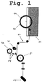
- Fig. 1 The embodiment shown in Fig. 1 is applied to the paper manufacture in a paper mill, wherein a security thread 1 is introduced in banknotes, for example.
- a security thread 1 is introduced in banknotes, for example.
- the invention is not restricted to this embodiment.
- the security thread 1 is constituted by a substrate which can be a tape or film, preferably of polyester.
- the substrate which usually is a transparent or printed polyester film, is metalized under vacuum with aluminium and/or copper etc. with a thickness from 6 to 50 ⁇ m.
- a suitable support material is applied, which can be quickly (preferably within a few milliseconds) brought from its solid state to a soft or "gum-like" state.
- thermoplastic material containing a resin having a low melting point (approximately 70 °C) is applied by painting, transferring, spraying, for example.
- a thermoplastic material wax, vinyl-polymer, polyurethane or any polymer or compound distributed in solvents on water basis or on solvent basis is suitable, provided that it has the capability to modify its state from solid to a soft or "gum-like" state.
- the amount of this material depends on the type and the capability of modifying its state.
- wax, vinyl-polymers, polymers or parafina can be put in a solvent based varnish and applied on the film.
- the thermoplastic material can be subjected to a roll embossing or stencil printing process wherein the thickness of deposition in a dried state is approximately 10 ⁇ m.
- thermoplastic material In order to enhance the adhesion of the thermoplastic material, a special treatment for enhancing the adhesion can be carried out before applying the thermoplastic material.
- the varnish Once the varnish has been applied and dried, it provides a sealing to the atmosphere, and the film is cut in stripes having a width of approximately 0.5 to 6 mm, particularly if the thread 1 shall be introduced within the paper by means of a total embedding or windows technique.
- the film is kept in larger sizes, if the film is transformed into tapes and is, therefore, applied on the surface of another final support.
- the thread 1 preferably has a width of 2.5 mm which is necessary to accommodate a microchip 2, because a conventional microchip 2 has side lengths of 0.5 mm to 1.5 mm.
- the threads 1 After cutting the film into threads 1, the threads 1 are winded up around bobbins (not shown) as they are usually used for the security threads 1.
- the thus winded thread 1 is positioned on appropriate reels 3 which comprise a motor spindle that winds off the thread 1 in a controlled manner so as to maintain a constant output.
- the thread 1 By winding off the thread 1, the thread 1 is heated by means of a contact with a heat cylinder 4.
- the method of heating and of modifying the state of the varnish can also be a mechanic operation by means of a contact of the polyester with a heat source 4, for example.
- the thread 1 is radiated by a beam that emits heat such as a laser beam, an infrared beam or an ultraviolet beam (not shown).
- the microchip 2 falls from an appropriate distributor 5 onto the thread 1, wherein the microchip 2 falling on the thread 1 is embedded therein.
- a curing process of the support material is performed, preferably by cooling the support material.
- the compound returns to its solid state and holds and supports the microchip 2.
- the cooling process can be performed in various ways.
- the thread 1 is supplied together with the microchip 2 in the interior of a paper compound 7 when the paper is produced.
- the start of the impulses for the fall of the microchip 2 from the distributor 5 and the cooling process are controlled by the detection of a corresponding notch 8 in a watermark cylinder 9, for example.
- the microchip 2 is introduced in register with the watermark of the banknote.
- the control means any conventional means known in the field of the paper manufacture can be used.
- a pressing means (not shown) that provides two rubber layers or two rubber cylinders spaced to each other by a fixed gap there between and which compress the microchip 2 into the varnish until the microchip 2 is embedded therein.
- the polyester substrate may have a thickness of 10 ⁇ m, on which aluminium is deposited under vacuum with a thickness of 0.2 ⁇ m.
- a vinyl protecting varnish is applied which has a thickness of approximately 2 ⁇ m.
- a heat-sensitive varnish is applied so as to obtain a layer of 10 ⁇ m of the heat-sensitive varnish in the dried state.
- the total thickness of the thread 1 is approximately 22 to 23 ⁇ m.
- the microchip 2 when the heat-sensitive varnish is activated and when the microchip 2 falls on it which has a thickness of 60 ⁇ m, for example, the microchip 2 can be embedded a few ⁇ m.
- thread 1 is optionally passed between two cylinders (not shown) of the pressing means which are spaced to each other with a gap of 75 ⁇ m so that that the microchip 2 is embedded for at least 8 to 9 ⁇ m into the heat-sensitive varnish.
- the advantage of the invention is the possibility to position the microchip 2 at a variable distance. Thereby, it is not necessary to use a pre-constructed thread magazine, for instance, which would involve excessive costs.
- the thread 1 suitable for accommodating the microchip 2 and the microchip 2 itself are the same for all banknotes independently from the kind of the banknotes.
- data or signals are programmable and machine-readable from the security thread 1.
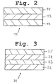
- Fig. 2 shows a thread 11 comprising a substrate 12 of polyester or polypropylene.
- a medium layer 13 is applied which carries specific characters, signs, data or any other information which are helpful for an individualisation of a document in which the thread 11 is to be inserted.
- the medium layer 13 preferably has a thickness of 6 to 50 ⁇ m.
- This medium layer 13 may comprise a varnish or coloured inks (red, green, blue, yellow, for instance).
- the varnishes or inks may be applied sequentially and/or completely or partially overlapping.
- the varnish or ink may be mixed with the substrate of polymer.
- the medium layer 13 may absorb.light having long or short wavelengths (about 360 nm or 254 nm).
- the medium layer 13 may comprises a fluorescent dye.
- the medium layer 13 may comprise a varnish or an ink which exhibits a chromatic variation according to the diffraction angle.
- the varnish or the ink can be applied sequentially and/or completely or partially overlapping.
- the medium layer 13 may comprise a magnetic ink having different coercitivities by applying the magnetic ink continuously, discontinuously or in a manner like SISMA which is a Mantegazza Patent.
- the medium layer 13 may comprise images or holograms of any type, i.e. exelgrams, pixelgrams, dot matrix, depicted in a two dimensional or three dimensional manner.
- the medium layer 13 may comprise a metallic material which may be applied under vacuum such as aluminium, copper, nickel having a characteristic of reflecting light or a larger gloss. It is obvious that the metallic materials may be applied in different quantities, thickness' and types.
- the medium layer 13 constituted by any one of the above-mentioned with interruptions or even a partly lack of material.
- the materials may be applied in a negative or positive manner.
- the medium layer 13 may comprise substances for checking the magnetoresistance or an inductivity such as "Micro Tag".
- the medium layer 13 may comprise a varnish or an ink being conductive, transparent (for example polyaniline) or visual (for example a silver-based varnish or ink).
- a varnish or an ink being conductive, transparent (for example polyaniline) or visual (for example a silver-based varnish or ink).
- a heat-sensitive support material 14 is applied on the medium layer 13, as it is described above.
- the heat-sensitive material 14 is a thermoplastic having a thickness of about 10 ⁇ m.
- Fig. 3 shows a structural view of a thread 21 according to another embodiment of the invention.
- the thread 21 includes the substrate 22 and the medium layer 23 in a same way as the thread 11 shown in Fig. 2.
- an adhesive support material or a glue support material 24 is applied on the medium layer 23.
- the adhesive support material 24 may have a thickness of about 8 ⁇ m.
- the microchip 2 is adhered to the adhesive support material 24.
- an additional siliconated layer 25 is applied on the adhesive support material 24.
- the siliconated layer 25 may comprise paper with a density of 45 to 90 g/m 2 or polyester having a thickness of 10 to 20 ⁇ m.
- the siliconated layer 25 can alternatively be applied on that side of the thread 21 which is opposite of the adhesive support material 24. This is advantageously in particular when the thread 21 is winded up around a bobbin (in general, the siliconated layer 25 may also be provided on the heat-sensitive material 24 of the thread according to the embodiment shown in Fig. 2).
- a thread may comprise both the heat-sensitive support material 14 and the adhesive support material 24.
- the microchip 2 may comprise an antenna (not shown) for a wireless data transmission.
Landscapes
- Credit Cards Or The Like (AREA)
- Paper (AREA)
- Manufacture Of Switches (AREA)
- Yarns And Mechanical Finishing Of Yarns Or Ropes (AREA)
Abstract
Description
- The present invention relates to a method of manufacturing a security thread equipped with a microchip, a security thread, and a document comprising the thread.
- It is already known to provide a document such as a bank note with a security thread in order to provide a possibility to verify whether the banknote is genuine or not. A method of manufacturing of such a security thread is disclosed in the Italian Patent Application MI2001A001914. For the public use, such security thread allows a simple visual examination.
- However, it remains a need to provide the banknote with machine-readable information.
- DE 198 33 746 A1 discloses a generic security thread comprising a substrate, a support material provided on the substrate, a microchip fixedly attached to or at least partly embedded in the support material.
- EP-1 254 765 A1 discloses a further security thread without any microchip.
- It is the object of the present invention, to provide a method of manufacturing a security thread and a generic security thread which enable variable positioning of the microchip at a variable distance.
- This object is solved by the method of manufacturing a security thread having the features of claim 1 and by the security thread having the features of
claim 9. - The invention is further developed as it is defined in the dependent claims.
- With the continuous progress of the technology, particularly of the miniaturisation technique of microprocessors, a microchip has been developed which has a suitable dimension for the use in plastic or paper documents.
- Advantageously, the invention provides a method for precisely depositing such a microchip into a security thread, and also a security thread which is capable to accommodate the microchip. Thereby, the microchip is fixedly attached to or embedded in the thread. The security thus manufactured is suitable for banknotes, passports or passenger tickets, for instance.
- Advantageously, the deposition of the microchip can be carried out in a paper mill during the production of the paper. The security thread having the microchip incorporated therein can be introduced into the paper by means of a conventional system as it is used in a paper mill.
- In the following, the invention is described on the basis of preferred embodiments thereof with reference to the figures.
- Fig. 1 shows a method of manufacturing a security thread equipped with a microchip according to an embodiment of the invention;
- Fig. 2 shows a structural view of a thread according to an embodiment of the invention; and
- Fig. 3 shows a structural view of a thread according to another embodiment of the invention.
- The embodiment shown in Fig. 1 is applied to the paper manufacture in a paper mill, wherein a security thread 1 is introduced in banknotes, for example. However, the invention is not restricted to this embodiment.
- The security thread 1 is constituted by a substrate which can be a tape or film, preferably of polyester.
- In a first step, the substrate, which usually is a transparent or printed polyester film, is metalized under vacuum with aluminium and/or copper etc. with a thickness from 6 to 50 µm.
- Thereafter, on at least one side of the substrate, a suitable support material is applied, which can be quickly (preferably within a few milliseconds) brought from its solid state to a soft or "gum-like" state.
- As the support material, a thermoplastic material containing a resin having a low melting point (approximately 70 °C) is applied by painting, transferring, spraying, for example. In more detail, as the thermoplastic material, wax, vinyl-polymer, polyurethane or any polymer or compound distributed in solvents on water basis or on solvent basis is suitable, provided that it has the capability to modify its state from solid to a soft or "gum-like" state. The amount of this material depends on the type and the capability of modifying its state. For example, wax, vinyl-polymers, polymers or parafina can be put in a solvent based varnish and applied on the film. Optionally, the thermoplastic material can be subjected to a roll embossing or stencil printing process wherein the thickness of deposition in a dried state is approximately 10 µm.
- In order to enhance the adhesion of the thermoplastic material, a special treatment for enhancing the adhesion can be carried out before applying the thermoplastic material.
- Once the varnish has been applied and dried, it provides a sealing to the atmosphere, and the film is cut in stripes having a width of approximately 0.5 to 6 mm, particularly if the thread 1 shall be introduced within the paper by means of a total embedding or windows technique.
- Alternatively, the film is kept in larger sizes, if the film is transformed into tapes and is, therefore, applied on the surface of another final support.
- If the thread 1 shall be introduced in the paper together with the
microchip 2, the thread 1 preferably has a width of 2.5 mm which is necessary to accommodate amicrochip 2, because aconventional microchip 2 has side lengths of 0.5 mm to 1.5 mm. - After cutting the film into threads 1, the threads 1 are winded up around bobbins (not shown) as they are usually used for the security threads 1.
- The thus winded thread 1 is positioned on
appropriate reels 3 which comprise a motor spindle that winds off the thread 1 in a controlled manner so as to maintain a constant output. - By winding off the thread 1, the thread 1 is heated by means of a contact with a
heat cylinder 4. The method of heating and of modifying the state of the varnish can also be a mechanic operation by means of a contact of the polyester with aheat source 4, for example. Alternatively, the thread 1 is radiated by a beam that emits heat such as a laser beam, an infrared beam or an ultraviolet beam (not shown). - Considering the heat-sensitive characteristic of waxes, several 10 µm of the previously deposited compound are softened (it is obvious that the softening can be performed by any heating system).
- After the softening, the
microchip 2 falls from an appropriate distributor 5 onto the thread 1, wherein themicrochip 2 falling on the thread 1 is embedded therein. - When the microchip is appropriately deposited, a curing process of the support material is performed, preferably by cooling the support material. Directly after the cooling process by an air cooling means 6, the compound returns to its solid state and holds and supports the
microchip 2. Also in this case, the cooling process can be performed in various ways. - At this point, the thread 1 is supplied together with the
microchip 2 in the interior of apaper compound 7 when the paper is produced. - In this embodiment of the paper manufacture, the start of the impulses for the fall of the
microchip 2 from the distributor 5 and the cooling process are controlled by the detection of acorresponding notch 8 in awatermark cylinder 9, for example. Thereby, themicrochip 2 is introduced in register with the watermark of the banknote. As for the control means, any conventional means known in the field of the paper manufacture can be used. - Depending from the speed with which the paper is manufactured, and from the relative thickness of the varnish, when the varnish is still in the gum-like state and has already the
microchip 2 deposited thereon, it may be used a pressing means (not shown) that provides two rubber layers or two rubber cylinders spaced to each other by a fixed gap there between and which compress themicrochip 2 into the varnish until themicrochip 2 is embedded therein. - As a numeric example, the polyester substrate may have a thickness of 10 µm, on which aluminium is deposited under vacuum with a thickness of 0.2 µm. On the aluminium, a vinyl protecting varnish is applied which has a thickness of approximately 2 µm. On the protecting layer, a heat-sensitive varnish is applied so as to obtain a layer of 10 µm of the heat-sensitive varnish in the dried state. As a result, the total thickness of the thread 1 is approximately 22 to 23 µm.
- when the heat-sensitive varnish is activated and when the
microchip 2 falls on it which has a thickness of 60 µm, for example, themicrochip 2 can be embedded a few µm. - Then, thread 1 is optionally passed between two cylinders (not shown) of the pressing means which are spaced to each other with a gap of 75 µm so that that the
microchip 2 is embedded for at least 8 to 9 µm into the heat-sensitive varnish. - It is obvious that the preferred numeral values can be varied according to the materials which are used, in particular the target material that thereafter will receive the thread 1 with the embedded
microchip 2. - The advantage of the invention is the possibility to position the
microchip 2 at a variable distance. Thereby, it is not necessary to use a pre-constructed thread magazine, for instance, which would involve excessive costs. Moreover, the thread 1 suitable for accommodating themicrochip 2 and themicrochip 2 itself are the same for all banknotes independently from the kind of the banknotes. On the other hand, during the manufacturing process in the paper mill, data or signals are programmable and machine-readable from the security thread 1. - In the following, embodiments of the structure of the thread will be described with reference to Figs. 2 and 3. As an alternative to the thread 1 used in the embodiment of Fig. 1, the thread can be embodied in the following manner.
- Fig. 2 shows a
thread 11 comprising asubstrate 12 of polyester or polypropylene. - On the
substrate 12, amedium layer 13 is applied which carries specific characters, signs, data or any other information which are helpful for an individualisation of a document in which thethread 11 is to be inserted. Themedium layer 13 preferably has a thickness of 6 to 50 µm. - This
medium layer 13 may comprise a varnish or coloured inks (red, green, blue, yellow, for instance). The varnishes or inks may be applied sequentially and/or completely or partially overlapping. Alternatively, the varnish or ink may be mixed with the substrate of polymer. Themedium layer 13 may absorb.light having long or short wavelengths (about 360 nm or 254 nm). Themedium layer 13 may comprises a fluorescent dye. - Alternatively, the
medium layer 13 may comprise a varnish or an ink which exhibits a chromatic variation according to the diffraction angle. Also in this case, the varnish or the ink can be applied sequentially and/or completely or partially overlapping. - Alternatively, the
medium layer 13 may comprise a magnetic ink having different coercitivities by applying the magnetic ink continuously, discontinuously or in a manner like SISMA which is a Mantegazza Patent. - Alternatively, the
medium layer 13 may comprise images or holograms of any type, i.e. exelgrams, pixelgrams, dot matrix, depicted in a two dimensional or three dimensional manner. - Alternatively, the
medium layer 13 may comprise a metallic material which may be applied under vacuum such as aluminium, copper, nickel having a characteristic of reflecting light or a larger gloss. It is obvious that the metallic materials may be applied in different quantities, thickness' and types. - The
medium layer 13 constituted by any one of the above-mentioned with interruptions or even a partly lack of material. The materials may be applied in a negative or positive manner. - Alternatively, the
medium layer 13 may comprise substances for checking the magnetoresistance or an inductivity such as "Micro Tag". - Alternatively, the
medium layer 13 may comprise a varnish or an ink being conductive, transparent (for example polyaniline) or visual (for example a silver-based varnish or ink). - On the
medium layer 13, as it is described above, a heat-sensitive support material 14 is applied. Preferably, the heat-sensitive material 14 is a thermoplastic having a thickness of about 10 µm. - Fig. 3 shows a structural view of a
thread 21 according to another embodiment of the invention. - The
thread 21 according to this embodiment includes the substrate 22 and themedium layer 23 in a same way as thethread 11 shown in Fig. 2. - Instead of the heat-sensitive support material, an adhesive support material or a
glue support material 24 is applied on themedium layer 23. Theadhesive support material 24 may have a thickness of about 8 µm. Themicrochip 2 is adhered to theadhesive support material 24. - Preferably, an
additional siliconated layer 25 is applied on theadhesive support material 24. Thesiliconated layer 25 may comprise paper with a density of 45 to 90 g/m2 or polyester having a thickness of 10 to 20 µm. Although it is not shown in the figures, thesiliconated layer 25 can alternatively be applied on that side of thethread 21 which is opposite of theadhesive support material 24. This is advantageously in particular when thethread 21 is winded up around a bobbin (in general, thesiliconated layer 25 may also be provided on the heat-sensitive material 24 of the thread according to the embodiment shown in Fig. 2). - Alternatively, a thread may comprise both the heat-
sensitive support material 14 and theadhesive support material 24. - The invention has been described with reference to the preferred embodiment. However, it is obvious for the skilled person that the invention can be modified in various ways. Such modifications are also within the scope of protection which is defined by the claims.
- For example, the
microchip 2 may comprise an antenna (not shown) for a wireless data transmission.
Claims (12)
- A method of manufacturing a security thread or strip (1; 11) having a microchip (2), comprising the steps of:providing a support material (14) on a substrate (12,13);softening said support material (14), preferably by heating said support material (14);depositing a microchip (2) on or at least partly in the softened support material (14); andcuring said support material (14), preferably by cooling said support material (14).
- The method of manufacturing, a security thread (1; 11) according to claim 1, wherein said support material (14) is a heat-sensitive material, preferably a thermoplastic material containing a resin having a low melting point, such as wax, vinyl-polymer, polyurethane or any polymer or compound distributed in water based solvents or in any solvent that has the characteristic to modify its state from solid to soft.
- The method of manufacturing a security thread (1) according to claim 1 or 2, wherein, in the step of softening said support material (14), the support material (14) is heated by a contact with a heating means (4) or by heat radiation, preferably by an infrared beam, and ultraviolet beam or a laser beam.
- The method of manufacturing a security thread (1; 11) according to one of the preceding claims, wherein, in the step of depositing said microchip (2), the microchip (2) falls on the softened support material (14) and sinks at least partly into the support material (14) by its own gravity.
- The method of manufacturing a security thread (1; 11) according to one of the preceding claims, wherein, in the step of depositing said microchip (2), said microchip (2) is positioned on the support material (14), and thereafter, when the support material (14) is still soft, the microchip (2) is pressed into the support material (14) by a pressing means.
- The method of manufacturing a security thread (1; 11) according to one of the preceding claims, comprising a step of winding up the security thread (1) around a spool (9).
- The method of manufacturing a security thread (1; 11) according to claim 6, wherein a timing of softening said support material (14), depositing said microchip (2) and/or curing said support material (14) is set in accordance to a winding operation of the spool (9).
- The method of manufacturing a security thread (1) according to one of claims 6 or 7, wherein said spool (9) is a watermarking cylinder (9) which has register notches (8) and transports the security thread (1) into a paper compound (7), and said timing of softening said support material (14), depositing said microchip (2) and/or curing said support material (14) is set in accordance to a detection of said register notches (8).
- A security thread (1; 11; 21) comprisinga substrate (12; 22), preferably of polyester;a support material (14; 24) provided on the substrate (12; 22),a microchip (2) fixedly attached to or at least partlyembedded in the support material (14; 24),characterized in that
the support material (14; 24) is a heat-sensitive material or an adhesive or glue material (24) which is preferably permanently active, wherein a siliconated layer (25) is removably deposited on the adhesive or glue material (24), or wherein a siliconated layer (25) is deposited on the side of the thread (1; 11; 21) which is opposite to the adhesive or glue material (24). - The security thread (1; 11; 21) according to claim 9, wherein the microchip (2) comprises an antenna for contactless data transfer.
- The security thread (1; 11; 21) according to claim 9, wherein the thread (1; 11; 21) comprises, preferably between the substrate (12; 22) and the support material (14; 24), a medium layer (13; 23) which carries specific characters, signs, holograms, data or any other information on a magnetic medium, metallic medium, fluorescent medium, printed medium or any other medium.
- A document, preferable a paper document, comprising said security thread (1; 11; 21) according to any one of claims 9 to 11.
Applications Claiming Priority (1)
| Application Number | Priority Date | Filing Date | Title |
|---|---|---|---|
| PCT/EP2002/012643 WO2004043706A1 (en) | 2002-11-12 | 2002-11-12 | Method of manufacturing a security thread having an embedded microchip, security thread and document comprising the thread |
Publications (2)
| Publication Number | Publication Date |
|---|---|
| EP1560718A1 EP1560718A1 (en) | 2005-08-10 |
| EP1560718B1 true EP1560718B1 (en) | 2007-03-28 |
Family
ID=32309288
Family Applications (1)
| Application Number | Title | Priority Date | Filing Date |
|---|---|---|---|
| EP02787657A Expired - Lifetime EP1560718B1 (en) | 2002-11-12 | 2002-11-12 | Method of manufacturing a security thread having an embedded microchip, security thread and document comprising the thread |
Country Status (7)
| Country | Link |
|---|---|
| US (1) | US7861937B2 (en) |
| EP (1) | EP1560718B1 (en) |
| AT (1) | ATE358028T1 (en) |
| AU (1) | AU2002351985A1 (en) |
| DE (1) | DE60219216T2 (en) |
| ES (1) | ES2282496T3 (en) |
| WO (1) | WO2004043706A1 (en) |
Cited By (4)
| Publication number | Priority date | Publication date | Assignee | Title |
|---|---|---|---|---|
| US9997102B2 (en) | 2016-04-19 | 2018-06-12 | X-Celeprint Limited | Wirelessly powered display and system |
| US10150326B2 (en) | 2016-02-29 | 2018-12-11 | X-Celeprint Limited | Hybrid document with variable state |
| US10150325B2 (en) | 2016-02-29 | 2018-12-11 | X-Celeprint Limited | Hybrid banknote with electronic indicia |
| US10217308B2 (en) | 2016-04-19 | 2019-02-26 | X-Celeprint Limited | Hybrid banknote with electronic indicia using near-field-communications |
Families Citing this family (4)
| Publication number | Priority date | Publication date | Assignee | Title |
|---|---|---|---|---|
| ITVR20040104A1 (en) * | 2004-06-16 | 2004-09-16 | Cartiere Fedrigoni & C Spa | EQUIPMENT FOR THE PRODUCTION OF SECURITY CARD AND RELATED PROCEDURE |
| FR2945551B1 (en) * | 2009-05-13 | 2011-08-26 | Oberthur Technologies | METHOD FOR MANUFACTURING A SECURITY ELEMENT FOR A SECURITY DOCUMENT |
| KR101874620B1 (en) * | 2012-02-28 | 2018-07-05 | 에이치피프린팅코리아 주식회사 | Security paper for being detectable by metal detectors |
| DE102021111894A1 (en) * | 2021-05-06 | 2022-11-10 | Mühlbauer ID Services GmbH | SECURITY DOCUMENT WITH THREAD-LIKE SECURITY ELEMENT AND METHOD AND DEVICE FOR ITS MANUFACTURE |
Family Cites Families (8)
| Publication number | Priority date | Publication date | Assignee | Title |
|---|---|---|---|---|
| US3943685A (en) * | 1974-07-19 | 1976-03-16 | Illinois Tool Works Inc. | Machine for loading electric components into a carrier strip |
| US5486022A (en) * | 1994-04-04 | 1996-01-23 | Crane & Co., Inc. | Security threads having at least two security detection features and security papers employing same |
| DE19630648A1 (en) * | 1996-07-30 | 1998-02-05 | Diehl Gmbh & Co | Banknote with increased security against forgery |
| SE9701612D0 (en) * | 1997-04-29 | 1997-04-29 | Johan Asplund | Smartcard and method for its manufacture |
| NL1008929C2 (en) * | 1998-04-20 | 1999-10-21 | Vhp Ugchelen Bv | Substrate made of paper provided with an integrated circuit. |
| DE19833746A1 (en) * | 1998-07-27 | 2000-02-03 | Joergen Brosow | Security paper and method for checking authenticity of documents recorded on it protects securities like bank notes against forgery by using embedded electronic switching circuit |
| GB2375078A (en) | 2001-04-30 | 2002-11-06 | Rue De Int Ltd | Security substrate with indicia only viewable in transmitted light |
| FR2827986B1 (en) * | 2001-07-30 | 2004-04-02 | Arjo Wiggins Sa | METHOD OF MANUFACTURING AN ARTICLE INCLUDING A FIBROUS LAYER AND AT LEAST ONE ELECTRONIC CHIP, AND ARTICLE THUS OBTAINED |
-
2002
- 2002-11-12 ES ES02787657T patent/ES2282496T3/en not_active Expired - Lifetime
- 2002-11-12 US US10/534,617 patent/US7861937B2/en not_active Expired - Fee Related
- 2002-11-12 DE DE60219216T patent/DE60219216T2/en not_active Expired - Lifetime
- 2002-11-12 WO PCT/EP2002/012643 patent/WO2004043706A1/en not_active Ceased
- 2002-11-12 AU AU2002351985A patent/AU2002351985A1/en not_active Abandoned
- 2002-11-12 AT AT02787657T patent/ATE358028T1/en active
- 2002-11-12 EP EP02787657A patent/EP1560718B1/en not_active Expired - Lifetime
Cited By (5)
| Publication number | Priority date | Publication date | Assignee | Title |
|---|---|---|---|---|
| US10150326B2 (en) | 2016-02-29 | 2018-12-11 | X-Celeprint Limited | Hybrid document with variable state |
| US10150325B2 (en) | 2016-02-29 | 2018-12-11 | X-Celeprint Limited | Hybrid banknote with electronic indicia |
| US10675905B2 (en) | 2016-02-29 | 2020-06-09 | X-Celeprint Limited | Hybrid banknote with electronic indicia |
| US9997102B2 (en) | 2016-04-19 | 2018-06-12 | X-Celeprint Limited | Wirelessly powered display and system |
| US10217308B2 (en) | 2016-04-19 | 2019-02-26 | X-Celeprint Limited | Hybrid banknote with electronic indicia using near-field-communications |
Also Published As
| Publication number | Publication date |
|---|---|
| US7861937B2 (en) | 2011-01-04 |
| ATE358028T1 (en) | 2007-04-15 |
| ES2282496T3 (en) | 2007-10-16 |
| US20060152362A1 (en) | 2006-07-13 |
| WO2004043706A1 (en) | 2004-05-27 |
| DE60219216D1 (en) | 2007-05-10 |
| DE60219216T2 (en) | 2008-01-03 |
| EP1560718A1 (en) | 2005-08-10 |
| AU2002351985A1 (en) | 2004-06-03 |
Similar Documents
| Publication | Publication Date | Title |
|---|---|---|
| EP0538358B1 (en) | Improvements relating to signature panels | |
| CA2035432C (en) | A paper of value having an optically variable security element | |
| US5438928A (en) | Signature panels | |
| CN101084124B (en) | Processes and products for making laminated sheets | |
| JP7610984B2 (en) | Method for manufacturing laminate and laminate film, laminate and laminate film | |
| AU2004293251A1 (en) | Security printing using a diffraction grating | |
| JP2014522328A (en) | Hot stamp method and apparatus | |
| WO1999055530A1 (en) | Refractive overlaminate panel technique for the production of identification cards | |
| CN1341053A (en) | Method for producing multi-layer security products and security product produced according to this method | |
| EP1560718B1 (en) | Method of manufacturing a security thread having an embedded microchip, security thread and document comprising the thread | |
| US8654405B2 (en) | Method for producing a multi-layered film | |
| EP0626909B1 (en) | Transfer method and device | |
| JP2003335083A (en) | Print recording medium, commuter pass, and manufacturing method thereof | |
| JP4962386B2 (en) | Patch intermediate transfer recording medium and anti-counterfeit medium using the same | |
| US20220355607A1 (en) | A smart and secure label stock | |
| JP4391081B2 (en) | Thermal printing recording medium, commuter pass, and manufacturing method thereof | |
| EP2411232B1 (en) | Forgery-resistant document, such as a banknote, a passport, an identity card, and a manufacturing method thereof | |
| US20250187360A1 (en) | Smart and secure label stock | |
| JP2004188799A (en) | card | |
| AU2013201941A1 (en) | Security printing using a diffraction grating | |
| JPH0698861B2 (en) | Method of manufacturing document substrate requiring authenticity | |
| GB2275653A (en) | Ticket with foil on colour-forming thermal substrate | |
| CN103930905A (en) | Security film comprising a radio frequency readable code |
Legal Events
| Date | Code | Title | Description |
|---|---|---|---|
| PUAI | Public reference made under article 153(3) epc to a published international application that has entered the european phase |
Free format text: ORIGINAL CODE: 0009012 |
|
| 17P | Request for examination filed |
Effective date: 20050504 |
|
| AK | Designated contracting states |
Kind code of ref document: A1 Designated state(s): AT BE BG CH CY CZ DE DK EE ES FI FR GB GR IE IT LI LU MC NL PT SE SK TR |
|
| AX | Request for extension of the european patent |
Extension state: AL LT LV MK RO SI |
|
| RAP1 | Party data changed (applicant data changed or rights of an application transferred) |
Owner name: FABRIANO SECURITIES S.R.L. |
|
| DAX | Request for extension of the european patent (deleted) | ||
| GRAP | Despatch of communication of intention to grant a patent |
Free format text: ORIGINAL CODE: EPIDOSNIGR1 |
|
| GRAS | Grant fee paid |
Free format text: ORIGINAL CODE: EPIDOSNIGR3 |
|
| GRAA | (expected) grant |
Free format text: ORIGINAL CODE: 0009210 |
|
| AK | Designated contracting states |
Kind code of ref document: B1 Designated state(s): AT BE BG CH CY CZ DE DK EE ES FI FR GB GR IE IT LI LU MC NL PT SE SK TR |
|
| PG25 | Lapsed in a contracting state [announced via postgrant information from national office to epo] |
Ref country code: FI Free format text: LAPSE BECAUSE OF FAILURE TO SUBMIT A TRANSLATION OF THE DESCRIPTION OR TO PAY THE FEE WITHIN THE PRESCRIBED TIME-LIMIT Effective date: 20070328 Ref country code: BE Free format text: LAPSE BECAUSE OF FAILURE TO SUBMIT A TRANSLATION OF THE DESCRIPTION OR TO PAY THE FEE WITHIN THE PRESCRIBED TIME-LIMIT Effective date: 20070328 |
|
| REG | Reference to a national code |
Ref country code: GB Ref legal event code: FG4D |
|
| REG | Reference to a national code |
Ref country code: CH Ref legal event code: EP |
|
| REG | Reference to a national code |
Ref country code: SE Ref legal event code: TRGR |
|
| REF | Corresponds to: |
Ref document number: 60219216 Country of ref document: DE Date of ref document: 20070510 Kind code of ref document: P |
|
| REG | Reference to a national code |
Ref country code: IE Ref legal event code: FG4D |
|
| REG | Reference to a national code |
Ref country code: CH Ref legal event code: NV Representative=s name: NOVAGRAAF INTERNATIONAL SA |
|
| PG25 | Lapsed in a contracting state [announced via postgrant information from national office to epo] |
Ref country code: PT Free format text: LAPSE BECAUSE OF FAILURE TO SUBMIT A TRANSLATION OF THE DESCRIPTION OR TO PAY THE FEE WITHIN THE PRESCRIBED TIME-LIMIT Effective date: 20070828 |
|
| ET | Fr: translation filed | ||
| REG | Reference to a national code |
Ref country code: ES Ref legal event code: FG2A Ref document number: 2282496 Country of ref document: ES Kind code of ref document: T3 |
|
| PG25 | Lapsed in a contracting state [announced via postgrant information from national office to epo] |
Ref country code: SK Free format text: LAPSE BECAUSE OF FAILURE TO SUBMIT A TRANSLATION OF THE DESCRIPTION OR TO PAY THE FEE WITHIN THE PRESCRIBED TIME-LIMIT Effective date: 20070328 |
|
| PG25 | Lapsed in a contracting state [announced via postgrant information from national office to epo] |
Ref country code: CZ Free format text: LAPSE BECAUSE OF FAILURE TO SUBMIT A TRANSLATION OF THE DESCRIPTION OR TO PAY THE FEE WITHIN THE PRESCRIBED TIME-LIMIT Effective date: 20070328 |
|
| PG25 | Lapsed in a contracting state [announced via postgrant information from national office to epo] |
Ref country code: DK Free format text: LAPSE BECAUSE OF FAILURE TO SUBMIT A TRANSLATION OF THE DESCRIPTION OR TO PAY THE FEE WITHIN THE PRESCRIBED TIME-LIMIT Effective date: 20070328 |
|
| PLBE | No opposition filed within time limit |
Free format text: ORIGINAL CODE: 0009261 |
|
| STAA | Information on the status of an ep patent application or granted ep patent |
Free format text: STATUS: NO OPPOSITION FILED WITHIN TIME LIMIT |
|
| 26N | No opposition filed |
Effective date: 20080102 |
|
| PG25 | Lapsed in a contracting state [announced via postgrant information from national office to epo] |
Ref country code: GR Free format text: LAPSE BECAUSE OF FAILURE TO SUBMIT A TRANSLATION OF THE DESCRIPTION OR TO PAY THE FEE WITHIN THE PRESCRIBED TIME-LIMIT Effective date: 20070629 |
|
| PG25 | Lapsed in a contracting state [announced via postgrant information from national office to epo] |
Ref country code: MC Free format text: LAPSE BECAUSE OF NON-PAYMENT OF DUE FEES Effective date: 20071130 |
|
| PG25 | Lapsed in a contracting state [announced via postgrant information from national office to epo] |
Ref country code: IE Free format text: LAPSE BECAUSE OF NON-PAYMENT OF DUE FEES Effective date: 20071112 |
|
| PG25 | Lapsed in a contracting state [announced via postgrant information from national office to epo] |
Ref country code: EE Free format text: LAPSE BECAUSE OF FAILURE TO SUBMIT A TRANSLATION OF THE DESCRIPTION OR TO PAY THE FEE WITHIN THE PRESCRIBED TIME-LIMIT Effective date: 20070328 |
|
| PG25 | Lapsed in a contracting state [announced via postgrant information from national office to epo] |
Ref country code: CY Free format text: LAPSE BECAUSE OF FAILURE TO SUBMIT A TRANSLATION OF THE DESCRIPTION OR TO PAY THE FEE WITHIN THE PRESCRIBED TIME-LIMIT Effective date: 20070328 |
|
| PG25 | Lapsed in a contracting state [announced via postgrant information from national office to epo] |
Ref country code: LU Free format text: LAPSE BECAUSE OF NON-PAYMENT OF DUE FEES Effective date: 20071112 Ref country code: BG Free format text: LAPSE BECAUSE OF FAILURE TO SUBMIT A TRANSLATION OF THE DESCRIPTION OR TO PAY THE FEE WITHIN THE PRESCRIBED TIME-LIMIT Effective date: 20070628 |
|
| PG25 | Lapsed in a contracting state [announced via postgrant information from national office to epo] |
Ref country code: TR Free format text: LAPSE BECAUSE OF FAILURE TO SUBMIT A TRANSLATION OF THE DESCRIPTION OR TO PAY THE FEE WITHIN THE PRESCRIBED TIME-LIMIT Effective date: 20070328 |
|
| REG | Reference to a national code |
Ref country code: CH Ref legal event code: PFA Owner name: FABRIANO SECURITIES S.R.L. Free format text: FABRIANO SECURITIES S.R.L.#VIA MILANO, 71#20021 OSPIATE DI BOLLATE (IT) -TRANSFER TO- FABRIANO SECURITIES S.R.L.#VIA MILANO, 71#20021 OSPIATE DI BOLLATE (IT) |
|
| REG | Reference to a national code |
Ref country code: GB Ref legal event code: 732E Free format text: REGISTERED BETWEEN 20110901 AND 20110907 |
|
| REG | Reference to a national code |
Ref country code: CH Ref legal event code: PFA Owner name: FEDRIGONI S.P.A. Free format text: FEDRIGONI CARTIERE S.P.A.#STRADA DEL LINFANO N? 16#ARCO (TN) (IT) -TRANSFER TO- FEDRIGONI S.P.A.#VIALE PIAVE N? 3#37135 VERONA (IT) Ref country code: CH Ref legal event code: PFUS Owner name: FEDRIGONI CARTIERE S.P.A., IT Free format text: FORMER OWNER: FABRIANO SECURITIES S.R.L., IT |
|
| REG | Reference to a national code |
Ref country code: DE Ref legal event code: R082 Ref document number: 60219216 Country of ref document: DE Representative=s name: TBK, DE |
|
| REG | Reference to a national code |
Ref country code: FR Ref legal event code: TP Owner name: FEDRIGONI S.P.A., IT Effective date: 20121023 Ref country code: FR Ref legal event code: CA Effective date: 20121023 |
|
| REG | Reference to a national code |
Ref country code: ES Ref legal event code: PC2A Owner name: FEDRIGONI S.P.A. Effective date: 20121204 |
|
| REG | Reference to a national code |
Ref country code: DE Ref legal event code: R082 Ref document number: 60219216 Country of ref document: DE Representative=s name: TBK, DE Effective date: 20121106 Ref country code: DE Ref legal event code: R081 Ref document number: 60219216 Country of ref document: DE Owner name: FEDRIGONI S.P.A., IT Free format text: FORMER OWNER: FABRIANO SECURITIES S.R.L., OSPIATE DI BOLLATE, IT Effective date: 20121106 Ref country code: DE Ref legal event code: R081 Ref document number: 60219216 Country of ref document: DE Owner name: FEDRIGONI S.P.A., IT Free format text: FORMER OWNER: FABRIANO SECURITIES S.R.L., OSPIATE DI BOLLATE, MAILAND/MILANO, IT Effective date: 20121106 |
|
| REG | Reference to a national code |
Ref country code: AT Ref legal event code: PC Ref document number: 358028 Country of ref document: AT Kind code of ref document: T Owner name: FEDRIGONI CARTIERE S.P.A., IT Effective date: 20130201 |
|
| REG | Reference to a national code |
Ref country code: NL Ref legal event code: SD Effective date: 20130326 |
|
| REG | Reference to a national code |
Ref country code: FR Ref legal event code: PLFP Year of fee payment: 14 |
|
| REG | Reference to a national code |
Ref country code: FR Ref legal event code: PLFP Year of fee payment: 15 |
|
| REG | Reference to a national code |
Ref country code: AT Ref legal event code: HC Ref document number: 358028 Country of ref document: AT Kind code of ref document: T Owner name: FEDRIGONI S.P.A., IT Effective date: 20161219 |
|
| REG | Reference to a national code |
Ref country code: FR Ref legal event code: PLFP Year of fee payment: 16 |
|
| PGFP | Annual fee paid to national office [announced via postgrant information from national office to epo] |
Ref country code: NL Payment date: 20201119 Year of fee payment: 19 |
|
| PGFP | Annual fee paid to national office [announced via postgrant information from national office to epo] |
Ref country code: SE Payment date: 20201123 Year of fee payment: 19 Ref country code: ES Payment date: 20201214 Year of fee payment: 19 Ref country code: IT Payment date: 20201130 Year of fee payment: 19 Ref country code: DE Payment date: 20201127 Year of fee payment: 19 Ref country code: FR Payment date: 20201120 Year of fee payment: 19 Ref country code: CH Payment date: 20201124 Year of fee payment: 19 Ref country code: AT Payment date: 20201117 Year of fee payment: 19 Ref country code: GB Payment date: 20201123 Year of fee payment: 19 |
|
| REG | Reference to a national code |
Ref country code: DE Ref legal event code: R119 Ref document number: 60219216 Country of ref document: DE |
|
| REG | Reference to a national code |
Ref country code: CH Ref legal event code: PL |
|
| REG | Reference to a national code |
Ref country code: NL Ref legal event code: MM Effective date: 20211201 |
|
| REG | Reference to a national code |
Ref country code: AT Ref legal event code: MM01 Ref document number: 358028 Country of ref document: AT Kind code of ref document: T Effective date: 20211112 |
|
| GBPC | Gb: european patent ceased through non-payment of renewal fee |
Effective date: 20211112 |
|
| PG25 | Lapsed in a contracting state [announced via postgrant information from national office to epo] |
Ref country code: SE Free format text: LAPSE BECAUSE OF NON-PAYMENT OF DUE FEES Effective date: 20211113 |
|
| PG25 | Lapsed in a contracting state [announced via postgrant information from national office to epo] |
Ref country code: AT Free format text: LAPSE BECAUSE OF NON-PAYMENT OF DUE FEES Effective date: 20211112 |
|
| PG25 | Lapsed in a contracting state [announced via postgrant information from national office to epo] |
Ref country code: NL Free format text: LAPSE BECAUSE OF NON-PAYMENT OF DUE FEES Effective date: 20211201 |
|
| PG25 | Lapsed in a contracting state [announced via postgrant information from national office to epo] |
Ref country code: GB Free format text: LAPSE BECAUSE OF NON-PAYMENT OF DUE FEES Effective date: 20211112 Ref country code: DE Free format text: LAPSE BECAUSE OF NON-PAYMENT OF DUE FEES Effective date: 20220601 |
|
| PG25 | Lapsed in a contracting state [announced via postgrant information from national office to epo] |
Ref country code: FR Free format text: LAPSE BECAUSE OF NON-PAYMENT OF DUE FEES Effective date: 20211130 |
|
| PG25 | Lapsed in a contracting state [announced via postgrant information from national office to epo] |
Ref country code: IT Free format text: LAPSE BECAUSE OF NON-PAYMENT OF DUE FEES Effective date: 20211112 |
|
| REG | Reference to a national code |
Ref country code: ES Ref legal event code: FD2A Effective date: 20230210 |
|
| PG25 | Lapsed in a contracting state [announced via postgrant information from national office to epo] |
Ref country code: ES Free format text: LAPSE BECAUSE OF NON-PAYMENT OF DUE FEES Effective date: 20211113 |
|
| PG25 | Lapsed in a contracting state [announced via postgrant information from national office to epo] |
Ref country code: LI Free format text: LAPSE BECAUSE OF NON-PAYMENT OF DUE FEES Effective date: 20220630 Ref country code: CH Free format text: LAPSE BECAUSE OF NON-PAYMENT OF DUE FEES Effective date: 20220630 |