EP1560356B1 - Architektur mit dualen Filtern zur verminderten Dispersion - Google Patents
Architektur mit dualen Filtern zur verminderten Dispersion Download PDFInfo
- Publication number
- EP1560356B1 EP1560356B1 EP05300060A EP05300060A EP1560356B1 EP 1560356 B1 EP1560356 B1 EP 1560356B1 EP 05300060 A EP05300060 A EP 05300060A EP 05300060 A EP05300060 A EP 05300060A EP 1560356 B1 EP1560356 B1 EP 1560356B1
- Authority
- EP
- European Patent Office
- Prior art keywords
- dispersion
- channels
- thin film
- multiplexed channels
- transmitted
- Prior art date
- Legal status (The legal status is an assumption and is not a legal conclusion. Google has not performed a legal analysis and makes no representation as to the accuracy of the status listed.)
- Expired - Lifetime
Links
- 239000006185 dispersion Substances 0.000 title claims abstract description 167
- 239000010409 thin film Substances 0.000 claims abstract description 125
- 230000003287 optical effect Effects 0.000 claims description 19
- 238000000034 method Methods 0.000 claims description 18
- 238000001914 filtration Methods 0.000 claims description 3
- 230000005540 biological transmission Effects 0.000 abstract description 25
- 238000013461 design Methods 0.000 description 47
- 238000003780 insertion Methods 0.000 description 9
- 230000037431 insertion Effects 0.000 description 9
- 238000013459 approach Methods 0.000 description 4
- 230000000694 effects Effects 0.000 description 2
- 230000003116 impacting effect Effects 0.000 description 2
- 238000002955 isolation Methods 0.000 description 2
- 238000004806 packaging method and process Methods 0.000 description 2
- 230000009286 beneficial effect Effects 0.000 description 1
- 238000010276 construction Methods 0.000 description 1
- 230000002939 deleterious effect Effects 0.000 description 1
- 230000001419 dependent effect Effects 0.000 description 1
- 239000000835 fiber Substances 0.000 description 1
- 239000000945 filler Substances 0.000 description 1
- 238000004519 manufacturing process Methods 0.000 description 1
- 238000005259 measurement Methods 0.000 description 1
- 238000000926 separation method Methods 0.000 description 1
- 238000001228 spectrum Methods 0.000 description 1
Images


Classifications
-
- H—ELECTRICITY
- H04—ELECTRIC COMMUNICATION TECHNIQUE
- H04B—TRANSMISSION
- H04B10/00—Transmission systems employing electromagnetic waves other than radio-waves, e.g. infrared, visible or ultraviolet light, or employing corpuscular radiation, e.g. quantum communication
- H04B10/25—Arrangements specific to fibre transmission
- H04B10/2507—Arrangements specific to fibre transmission for the reduction or elimination of distortion or dispersion
- H04B10/2513—Arrangements specific to fibre transmission for the reduction or elimination of distortion or dispersion due to chromatic dispersion
- H04B10/25133—Arrangements specific to fibre transmission for the reduction or elimination of distortion or dispersion due to chromatic dispersion including a lumped electrical or optical dispersion compensator
Definitions
- Thin-film filter (TFF) devices are used for multiplexing/demultiplexing and adding/dropping WDM (Wavelength Division Multiplexed) channels in a multi-wavelength fiberoptic system.
- the thin-film devices are typically three-port devices that pass a particular wavelength (or range of wavelengths) in transmission depending on the construction of the optical filter element.
- Thin-film devices can also have fewer or more ports. If the input port contains a plurality of wavelengths, the transmission port passes one wavelength while the reflected port consists of all the remaining signals.
- demultiplexing the transmission port passes one wavelength while the reflected port consists of all the remaining signals.
- modules constructed from thin film devices can also be used to selectively add or drop single or multiple channels to dense WDM (DWDM) or coarse WDM (CWDM) systems. Channels can include single and/or multiple wavelengths, discrete and/or continuous.
- Another technique for reducing dispersion is by introducing a deliberate insertion loss ripple in the transmitted spectrum. Although this reduces dispersion it also trades-off the flatness of the passband (and hence the isolation in reflection).
- the other approach to lower dispersion is limited by the trade-off with other optical parameters. For example, higher ripple in the passband degrades the optical signal in particular for cases where this ripple adds up due to propagation through a number of mux/demux or add/drop modules.
- Various apparatuses and methods involve filtering a group of multiplexed channels.
- the group of multiplexed channels has a first adjacent channel spacing.
- the group of multiplexed channels includes a first and second subgroup of multiplexed channels.
- the first subgroup of multiplexed channels has a second adjacent channel spacing greater than the first adjacent channel spacing.
- the second subgroup of multiplexed channels has a third adjacent channel spacing greater than the first adjacent channel spacing.
- Some embodiments include first and second sets of thin film filters.
- Each thin film filter of the first set has no less than a first transmitted dispersion magnitude and no more than a first reflected dispersion magnitude.
- the first set splits the first subgroup of multiplexed channels from the group of multiplexed channels.
- Each thin film filter of the second set has no more than a second transmitted dispersion magnitude and no less than a second reflected dispersion magnitude.
- the second set splits the second subgroup of multiplexed channels from the group of multiplexed channels.
- the first transmitted dispersion magnitude exceeds the second transmitted dispersion magnitude.
- Some embodiments split the first subgroup of multiplexed channels from the group of multiplexed channels with a first set of thin film filters. Each thin film filter of the first set has no less than a first transmitted dispersion magnitude and no more than a first reflected dispersion magnitude. Some embodiments split the second subgroup of multiplexed channels from the group of multiplexed channels with a second set of thin film filters. Each thin film filter of the second set has no more than a second transmitted dispersion magnitude and no less than a second reflected dispersion magnitude. The first transmitted dispersion magnitude exceeds the second transmitted dispersion magnitude.
- Some embodiments split the first subgroup of multiplexed channels from the group of multiplexed channels with a first set of thin film filters. After splitting, each of the first group of multiplexed channels has no more than a first dispersion magnitude. The first dispersion magnitude can be substantially attributable to a first transmitted dispersion magnitude of a first set of thin film filters. Some embodiments split the second subgroup of multiplexed channels from the group of multiplexed channels with a second set of thin film filters. After splitting, each of the second group of multiplexed channels has no more than a second dispersion magnitude. The second dispersion magnitude can be substantially attributable to a first reflected dispersion magnitude of a first set of thin film filters and a second transmitted dispersion magnitude of a second set of thin film filters.
- Some embodiments split a group of preinterleaver multiplexed channels into at least a group of multiplexed channels and a second group of multiplexed channels. Some embodiments split the first subgroup of multiplexed channels from the group of multiplexed channels with a first set of thin film filters. After splitting, each of the first subgroup of multiplexed channels has no more than a first dispersion magnitude. The first dispersion magnitude can he substantially attributable to an interleaver dispersion magnitude and a first transmitted dispersion magnitude of a first set of thin film filters. Some embodiments split the second subgroup of multiplexed channels from the group of multiplexed channels with a second set of thin film filters.
- each of the second subgroup of multiplexed channels has no more than a second dispersion magnitude.
- the second dispersion magnitude can be substantially attributable to an interleaver dispersion magnitude, a first reflected dispersion magnitude of a first set of thin film filters, and a second transmitted dispersion magnitude of a second set of thin film filters.
- Some embodiments include first and second sets thin film filters.
- the first set of thin film filters split the first subgroup of multiplexed channels from the group of multiplexed channels.
- the second set of thin film filters split the second subgroup of multiplexed channels from the group of multiplexed channels. After the first subgroup of multiplexed channels and the second subgroup of multiplexed channels are split from the group of multiplexed channels, a first dispersion magnitude of the first subgroup of multiplexed channels is substantially equal to a second dispersion magnitude of the second subgroup of multiplexed channels.
- Some embodiments split a first subgroup of multiplexed channels from the group of multiplexed channels with a first set of thin film filters. Some embodiments split the second subgroup of multiplexed channels from the group of multiplexed channels with a second set of thin film filters. After the first subgroup of multiplexed channels and the second subgroup of multiplexed channels are split from the group of multiplexed channels, a first dispersion magnitude of the first subgroup of multiplexed channels is substantially equal to a second dispersion magnitude of the second subgroup of multiplexed channels.
- Figure 1 shows an example of a thin-film filter-based three port device.
- Figure 2 is an example of an architecture for demuxing eight channels.
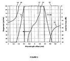
- Figure 3 shows a graph of dispersion and insertion loss variation for a thin film filter.
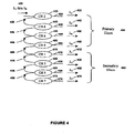
- Figure 4 shows an example of an architecture for demuxing eight channels.
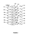
- Figure 5 shows an architecture for demuxing eight channels which includes an interleaver.
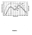
- Figure 6 shows a channel with worst-case dispersion for the architecture depicted in Fig. 5.
- the thin film filter includes an input port 120, a transmitted port 122, and a reflected port 124.
- the input port 120 receives multiple channels 130.
- the transmitted port 122 removes a single channel 132.
- the other channels 134 appear at the reflected port 124.
- Thin film filters suffer from chromatic dispersion (CD) in transmitted and reflected paths.
- CD chromatic dispersion
- the CD in an optical signal typically has a deleterious effect of expanding the pulse in time domain and hence resulting in increased inter-symbol interference (ISI). This degrades the capability to detect the signal at the receiver and hence optical modules for multiplexing or demultiplexing are typically designed to lower the overall dispersion for each of the WDM channels.
- the filters are arranged in order such that the channels are demuxed from the lowest to highest wavelength or from the highest to lowest wavelength.
- Thin film devices 210, 220, 230, 240, 250, 260, 270, and 280 are serially connected.
- the reflected port of thin film device 210 and the input port of thin film device 220 are connected at 216.
- the reflected port of thin film device 220 and the input port of thin film device 230 are connected at 226.
- the reflected port of thin film device 230 and the input port of thin film device 240 are connected at 236.
- the reflected port of thin film device 240 and the input port of thin film device 250 are connected at 246.
- the reflected port of thin film device 250 and the input port of thin film device 260 are connected at 256.
- the reflected port of thin film device 260 and the input port of thin film device 270 are connected at 266.
- the reflected port of thin film device 270 and the input port of thin film device 280 are connected at 276.
- the transmitted port 214 of thin film filter 210 removes the channel 212.
- the transmitted port 224 of thin film filter 220 removes the channel 222.
- the transmitted port 234 of thin film filter 230 removes the channel 232.
- the transmitted port 244 of thin film filter 240 removes the channel 242.
- the transmitted port 254 of thin film filter 250 removes the channel 252.
- the transmitted port 264 of thin film filter 260 removes the channel 262.
- the transmitted port 274 of thin film filter 270 removes the channel 272.
- the transmitted port 284 of thin film filter 280 removes the channel 282.
- the channels can be 100 GHz channels or wider or narrower channels.
- the thin film devices can be arranged from the shortest to longest wavelength, or from longest to shortest wavelength.
- the filters typically have the same design. In such a configuration the worst-case dispersion for a channel is the sum of the transmitted and reflected dispersion of the filter.
- Table 1 shows worst-case transmitted and reflected dispersion for four different filter designs. The difference from one design to the other arises from the variation of the index contrast between the high and low index alternating layers of the filter. All filters designs have five cavities. Other filter designs can have another number of cavities, such as 1, 2, 3, 4, or 6 or more.
- Table 1 shows the trade-off between the transmitted and reflected dispersion for filter designs using five cavities. The difference from one design to the other arises from the variation of the index contrast between the high and low index alternating layers of the filler. Designs in between the ones listed can also be achieved easily.
- the dispersion numbers are worst-case values in the ⁇ 17 GHz passband. As is evident the transmission dispersion increases from Design 1 to Design 4 while the reflected dispersion goes down.
- the lowest sum of transmission and reflected dispersion is ⁇ 25.1 ps/nm for Design 2. If one uses a standard architecture the first channel will only see the transmitted dispersion which for Design 2 is ⁇ 10.8 ps/nm. The remaining channels will have the reflected dispersion from the adjacent channel added and will result in an overall dispersion of ⁇ 25.1 ps/nm (sum of transmitted and reflected di spersion). In an architecture where the devices are arranged from lowest to highest wavelengths, the added reflected dispersions will only be negative. Hence, the overall dispersion for the other channels will be -25.1 ps/nm to +10.8 ps/nm, but the worst-case dispersion magnitude in the passband is 25.1 ps/nm.
- This worst-case dispersion magnitude will still be 25.1 ps/nm even if the devices are arranged from the highest to lowest wavelengths. Even by optimizing the design between the Designs 2 and 3 listed in Table 1, the overall sum of the transmitted and reflected dispersion will still be around ⁇ 25 ps/nm.
- Figure 3 shows a graph of dispersion and insertion loss variation for a thin film filter, in this example a 100 GHz filter. Dispersion corresponds to the left axis and insertion loss corresponds to the right axis. Design 3 from Table 1 is characterized.
- the vertical rectangular boxes 310, 312, and 314 represent the ⁇ 17 GHz ( ⁇ 0.136 nm) passband for the transmitted channel (312 is centered at zero wavelength offset) and the adjacent reflected channels (310 and 314 are centered at ⁇ 0.8 nm).
- the dispersion in the transmission band is shown within each such passband of ⁇ 17 GHz.
- the variation of dispersion in transmission 316 is negative to positive across the passband 312, being a minimum at the lowest edge of the passband, nominally zero in the middle of the passband, and highest at the upper edge of the passband.
- the variation of dispersion in reflection 316 is completely positive in the passband 310 on the shorter wavelength side.
- the variation of dispersion in reflection 316 is completely negative in the passband 314 on the longer wavelength side.
- the worst case dispersion in transmission is ⁇ 10.8 ps/nm while that in reflection is ⁇ 14.3 ps/nm. Insertion loss 318 is also shown.
- the typical passband requirement for many 100 GHz devices is ⁇ 10 GHz to ⁇ 14 GHz.
- Packaging of the filters into devices requires an extra margin of a few GHz to take care of over temperature operation and other packaging-related effects.
- the device passband is ⁇ 10 GHz while the extra margin is ⁇ 7 GHz.
- the transmission and reflection parameters hence are considered over a total passband of ⁇ 17 GHz at the filter level. In other embodiments, other total passbands, device passbands, and/or extra margins apply.
- the worst-case dispersion in transmission is ⁇ 10.8 ps/nm and ⁇ 14.3 ps/nm in reflection.
- the worst-case dispersion for this channel is ⁇ 10.8 ps/nm.
- the second channel not only is there a transmission through the second device, but also a reflection off the first one. Hence this channel accumulates dispersion in transmission and in reflection.
- the overall dispersion for the subsequent channels is a sum of the transmission and reflection, which for this design is ⁇ 25.1 ps/nm.
- the dispersion fur these subsequent channels can be non-symmetrical about the channel center wavelength.
- the magnitude of the positive and negative worst-case dispersion values is a function of the order of concatenation of the devices highest to lowest wavelength and lowest to highest wavelength. The dispersion magnitude is used as a figure of merit rather than the polarity of the dispersion in the operation of the system.
- the thin-film devices are arranged in a specific order in the module. This architecture first uses devices spaced by twice the input channel spacing of the channels. The remaining devices are placed subsequent to this to demux the other channels. For example, to demux an eight channel (numbered 1 through 8) 100 GHz system this technique would first demux all so called “even" channels (2,4,6.and 8). Once these channels are removed the remaining channels ("odd" -1,3,5 and 7) are then removed.
- the even channel filters are designed fur a higher dispersion in transmission but lower dispersion in reflection.
- the filters for the odd channels are designed such that the sum of the dispersion from the even channels (in reflection) and that from the odd channels (in transmission) is as low as possible. This ensures that the overall dispersion of the odd and even channels is lower than what one can achieve with the "standard" architecture.
- the modified architecture with dual-filer approach leads to a reduction of 30% in the worst-case dispersion magnitude compared with the standard architecture using a single filter.
- the advantage of many embodiments is that the chromatic dispersion of the module it is lowered without impacting other optical parameters.
- standard thin-film filters can be used, although specially designed filters (such as the ones with insertion loss ripple in the passband) can also be employed to further lower the dispersion. Also, this technique tends to provide the same worst-case dispersion magnitude for all channels of the module.
- FIG 4 an example of an architecture for demuxing eight channels is shown. Although 100 GHz channels are discussed, other embodiments use other types of channels. Thin film devices 420, 440, 460, 480, 410, 430, 450, and 470 are serially connected. The "even" channels are removed using the primary filters of thin film devices 420, 440, 460, and 480. The odd channels are removed subsequently using the secondary filters of thin film devices 410, 430, 450, and 470. The primary and secondary filters have different designs.
- the reflected port of thin film device 420 and the input port of thin film device 440 are connected at 426.
- the reflected port of thin film device 440 and the input port of thin film device 460 are connected at 446.
- the reflected port of thin fihn device 460 and the input port of thin film device 480 are connected at 466.
- the reflected port of thin film device 480 and the input port of thin film device 410 are connected at 486.
- the reflected port of thin film device 410 and the input port of thin film device 430 are connected at 416.
- the reflected port of thin film device 430 and the input port of thin film device 450 are connected at 436.
- the reflected port of thin film device 450 and the input port of thin film device 470 arc connected at 456.
- the transmitted port 424 of thin film filter 420 removes the channel 422.
- the transmitted port 444 of thin film filter 440 removes the channel 442.
- the transmitted port 464 of thin film filter 460 removes the channel 462.
- the transmitted port 484 of thin film filter 480 removes the channel 482.
- the transmitted port 414 of thin film filter 410 removes the channel 412.
- the transmitted port 434 of thin film filter 430 removes the channel 432.
- the transmitted port 454 of thin film filter 450 removes the channel 452.
- the transmitted port 474 of thin film filter 470 removes the channel 472.
- the "even" channels are first separated using the first filter design, the primary filter. Since these channels are spaced by twice the input channel separation, the reflected dispersion from the filters earlier in the chain has minimal impact. Hence the whole dispersion margin for that channel can be allocated to the transmitted dispersion of the primary filter.
- the primary filter can be designed to have a higher transmitted dispersion. If Design 4 from Table 1 is used for the primary filter, the "even" channels have a dispersion of ⁇ 17.6 ps/nm, which is the transmission dispersion of Design 4. Although channels after first transmitted channel have the impact of the reflected dispersion from the nonadjacent channel, this channel is 200 GHz away, which permits this effect to be neglected for practical purposes.
- the “odd” channels that remain after the removal of the "even” channels are spaced by 200 GHz. These channels are then separated using the second filter design, the secondary filter. These channels have two contributions to their overall chromatic dispersion - from the primary filters in reflection and from the secondary filters in transmission.
- a design for the primary filter that has a low dispersion in reflection was chosen (Design 4, ⁇ 9.9 ps/nm).
- Design 1 For the secondary filter, a design is chosen that meets all other optical parameters (such as bandwidths, isolation, etc.) while at the same time minimizing the transmitted dispersion. Of the four designs listed in Table 1, if Design 1 for the secondary filter yields the best results. Design 1 has a dispersion of ⁇ 8.3 ps/nm and ⁇ 18 ps/nm in reflection. The dispersion in reflection for the Secondary filter is irrelevant, although the value over the non-adjacent channel should be minimal.
- the worst-case dispersion then becomes ⁇ 17.2 ps/nm ( ⁇ 8.3 ps/nm from the secondary filter in transmission and ⁇ 9.9 ps/nm from the primary filter in reflection.
- the dispersion in reflection from the two primary filters on either side tends to offset each other slightly, resulting in a lower contribution from the primary filters.
- the worst-case dispersion can be reduced to ⁇ 17.6 ps/nm. This compares very favorably with the ⁇ 25.1 ps/nm worst-case dispersion one gets using the architecture where a single filter (e.g., Design 2) was used. This 30% reduction in dispersion is very beneficial for optical systems using thin-film-based mux/demux systems.
- the difference in the worst-case dispersion for the channels is less than ⁇ 1 ps/nm providing similar ISI penalty for all the channels.
- the difference in worst-case dispersion between the eight channels is almost as high as ⁇ 10.8 ps/nm.
- the consistency in the dispersion magnitude across all the channels is another advantage of the dual-filter technique.
- the dispersion can be improved even further by choosing better designs for primary and secondary filters. Also, if insertion loss ripple in the passband is not a concern, this two-filter configuration can be extended to devices made from specially designed filters that sacrifice a ripple for lower dispersion. That would potentially lead to even further reduction in the worst-case dispersion magnitude.
- the "odd” channels can be demuxed first, following which the "even” channels can be separated.
- the primary filter can used for the odd channels and the secondary filter for the even channels.
- the order of the filters can be reversed (from longest to shortest wavelength) for both odd and even channels without impacting the dispersion magnitude. This configuration can be extended to any channel spacing with systems that have three of more channels that need to be muxed, demuxed, added, or dropped.
- FIG. 5 an example of an architecture for demuxing eight channels which includes an interleaver is shown. Although 50 GHz channel are discussed, other embodiments use other types of channels.
- the interleaver receives channels 505 and splits them into even channels for thin film filters 520, 540, 560, and 580, and into odd channels for thin film filters 510, 550, 530, and 570.
- the even channels are handled by thin film devices 520, 560, 540, and 580, which are serially connected.
- the reflected port of thin film device 520 and the input port of thin film device 560 are connected at 526.
- the reflected port of thin film device 560 and the input port of thin film device 540 are connected at 566.
- the reflected port of thin film device 540 and the input port of thin film device 580 are connected at 546.
- the transmitted port 524 of thin film filter 520 removes the channel 522.
- the transmitted port 564 of thin film filter 560 removes the channel 562.
- the transmitted port 544 of thin film filter 540 removes the channel 542.
- the transmitted port 584 of thin film filter 580 removes the channel 582.
- the odd channels are handled by thin film devices 510, 550, 530, and 570, which are serially connected.
- the reflected port of thin film device 510 and the input port of thin film device 550 are connected at 516.
- the reflected port of thin film device 550 and the input port of thin film device 530 are connected at 556.
- the reflected port of thin film device 530 and the input port of thin film device 570 are connected at 536.
- the transmitted port 514 of thin film filter 510 removes the channel 512.
- the transmitted port 554 of thin film filter 550 removes the channel 552.
- the transmitted port 534 of thin film filter 530 removes the channel 532.
- the transmitted port 574 of thin film filter 570 removes the channel 572.
- the primary filters are used for channels 522, 562, 512, and 552.
- the secondary filters are used for channels 544, 584, 534, and 574.
- Interleavers are devices such as three port devices that in a demux configuration are used to separate odd and even channels.
- the input port contains a certain channel spacing, say 50 GHz, while the two output ports will contain the odd and even channels separately.
- the use of the interleaver enables one to double the channel spacing at the output ports and subsequently employ 100 GHz filters for demuxing.
- the 100 GHz devices are lower in cost and also provide a much lower chromatic dispersion than 50 GHz filters.
- the technique to use the dual-filter approach with an interleaver is illustrated in Fig 5. In one arm of the interleaver the non-adjacent even channels (channels 522 and 562) are separated first using primary filters while the secondary filters are used for the other even channels (channels 542 and 582).
- the odd channels are separated similarly (primary filters for channels 512 and 552 and secondary filters for channels 532 and 572).
- This configuration is a 50 GHz low-dispersion demux.
- the dispersion of the interleaver adds to the overall dispersion of the thin-film filters.
- Figure 6 shows the channel with the worst-case dispersion for the demux module employing the architecture depicted in Fig. 5. Insertion loss corresponds to the rights axis and is shown by curve 640.
- the three dispersion plots 610, 620, and 630 correspond to the left axis and show the measurements at three different operating temperatures (-5 °C, 25 °C and 70 °C).
- the worst case dispersion is ⁇ 30 ps/nm for this particular channel, highlighting the effectiveness of the dual-filter technique.
- the lowest value of the worst-case dispersion for the eight channels is ⁇ 20 ps/nm.
- the interleaver in this case had a channel-dependent dispersion of ⁇ 5 ps/nm to ⁇ 15 ps/nm.
- the data from this 50 GHz module shows the effectiveness of the dual-filter approach in not only reducing the worst-case dispersion but also in making the dispersion consistent from one channel to the other.
- the dispersion variation of ⁇ 10 ps/nm from the best-case to the worst-case channels can be attributed to the channel-to-channel dispersion variation of the interleaver..
Landscapes
- Physics & Mathematics (AREA)
- Electromagnetism (AREA)
- Engineering & Computer Science (AREA)
- Computer Networks & Wireless Communication (AREA)
- Signal Processing (AREA)
- Optical Filters (AREA)
- Optical Communication System (AREA)
- Filtration Of Liquid (AREA)
- Fluid-Pressure Circuits (AREA)
Claims (13)
- Optische Vorrichtung, wobei die optische Vorrichtung eine Mehrzahl von multiplexierten Kanälen (405), die einen ersten Nachbarkanalabstand besitzen, filtert,
wobei die Mehrzahl von multiplexierten Kanälen (405) wenigstens eine erste Untermehrzahl von multiplexierten Kanälen und eine zweite Untermehrzahl von multiplexierten Kanälen besitzt, wobei die erste Untermehrzahl von multiplexierten Kanälen einen zweiten Nachbarkanalabstand besitzt, der größer als der erste Nachbarkanalabstand ist, wobei die zweite Untermehrzahl von multiplexierten Kanälen einen dritten Nachbarkanalabstand besitzt, der größer als der erste Nachbarkanalabstand ist, wobei die optische Vorrichtung gekennzeichnet ist durch
einen ersten Satz aus einem oder aus mehreren Dünnschichtfiltern (490), wobei jedes Dünnschichtfilter des ersten Satzes aus einem oder aus mehreren Dünnschichtfiltern nicht weniger als einen ersten Durchlassdispersionsbetrag und nicht mehr als einen ersten Reflexionsdispersionsbetrag besitzt, wobei der erste Satz aus einem oder aus mehreren Dünnschichtfiltern (490) die erste Untermehrzahl von multiplexierten Kanälen unter den mehreren multiplexierten Kanälen aufteilt; und
einen zweiten Satz aus einem oder aus mehreren Dünnschichtfiltern (492), die nicht mehr als einen zweiten Durchlassdispersionsbetrag und nicht weniger als einen zweiten Reflexionsdispersionsbetrag besitzen,
wobei der zweite Satz aus einem oder aus mehreren Dünnschichtfiltern (492) die zweite Untermehrzahl von multiplexierten Kanälen unter den mehreren multiplexierten Kanälen (405) aufteilt,
wobei der erste Durchlassdispersionsbetrag den zweiten Durchlassdispersionsbetrag übersteigt. - Optische Vorrichtung nach Anspruch 1, wobei der erste Durchlassdispersionsbetrag, der erste Reflexionsdispersionsbetrag, der zweite Durchlassdispersionsbetrag und der zweite Reflexionsdispersionsbetrag Beträge für den schlechtesten Fall sind, die einem oder mehreren Durchlassbändern zugeordnet sind.
- Optische Vorrichtung nach Anspruch 1, wobei der zweite Nachbarkanalabstand und der dritte Nachbarkanalabstand gleich sind.
- Optische Vorrichtung nach Anspruch 1, wobei der zweite Nachbarkanalabstand und der dritte Nachbarkanalabstand unterschiedlich sind.
- Optische Vorrichtung nach Anspruch 1, wobei der erste Satz aus einem oder aus mehreren Dünnschichtfiltern vor dem zweiten Satz aus einem oder aus mehreren Dünnschichtfiltern angeordnet ist.
- Optische Vorrichtung nach Anspruch 1, die ferner umfasst:einen Verschachtler, der mehrere vor dem Verschachtler angeordnete multiplexierte Kanäle in wenigstens eine Gruppe von multiplexierten Kanälen und eine zweite Gruppe von multiplexierten Kanälen aufteilt.
- Optische Vorrichtung nach Anspruch 6, wobei die mehreren vor dem Verschachtler angeordneten multiplexierten Kanäle einen vierten Nachbarkanalabstand haben, der kleiner als der erste Nachbarkanalabstand ist.
- Verfahren zum Filtern einer Mehrzahl von multiplexierten Kanälen (405), die einen ersten Nachbarkanalabstand besitzen, wobei die Mehrzahl von multiplexierten Kanälen (405) wenigstens eine erste Untermehrzahl von multiplexierten Kanälen und eine zweite Untermehrzahl von multiplexierten Kanälen umfasst, wobei die erste Untermehrzahl von multiplexierten Kanälen einen zweiten Nachbarkanalabstand besitzt, der größer als der erste Nachbarkanalabstand ist, und wobei die zweite Untermehrzahl von benachbarten Kanälen einen dritten Nachbarkanalabstand besitzt, der größer als der erste Nachbarkanalabstand ist, wobei das Verfahren gekennzeichnet ist durch:Aufteilen der ersten Untermehrzahl von multiplexierten Kanälen unter den mehreren multiplexierten Kanälen mit einem ersten Satz aus einem oder ausmehreren Dünnschichtfiltern (490), derart, dass nach dem Aufteilen jeder der ersten Untermehrzahl von multiplexierten Kanälen nicht mehr als eine ersten Dispersionsbetrag hat, wobei der erste Dispersionsbetrag im Wesentlichen einem ersten Durchlassdispersionsbetrag des ersten Satzes aus einem oder aus mehreren Dünnschichtfiltern (490) zugeschrieben werden kann, undAufteilen der zweiten Untermehrzahl von multiplexierten Kanälen unter den mehreren multiplexierten Kanälen mit einem zweiten Satz aus einem oder aus mehreren Dünnschichtfiltern (492), derart, dass nach dem Aufteilen jeder der zweiten Untermehrzahl von multiplexierten Kanälen nicht mehr als einen zweiten Dispersionsbetrag hat, wobei der zweite Dispersionsbetrag im Wesentlichen einem ersten Reflexionsdispersionsbetrag des ersten Satzes aus einem oder aus mehreren Dünnschichtfiltern (490) und einem zweiten Durchlassdispersionsbetrag des zweiten Satzes aus einem oder aus mehreren Dünnschichtfiltern (492) zugeschrieben werden kann.
- Verfahren nach Anspruch 8, bei dem der erste Durchlassdispersionsbetrag den zweiten Durchlassdispersionsbetrag übersteigt.
- Verfahren nach Anspruch 8, bei dem der erste Dispersionsbetrag, der zweite Dispersionsbetrag, der erste Durchlassdispersionsbetrag, der erste Reflexionsdispersionsbetrag und der zweite Durchlassdispersionsbetrag Beträge für den schlechtesten Fall sind, die einem oder mehreren Durchlassbändern zugeordnet sind.
- Verfahren nach Anspruch 8, bei dem der zweite Nachbarkanalabstand und der dritte Nachbarkanalabstand gleich sind.
- Verfahren nach Anspruch 8, bei dem der zweite Nachbarkanalabstand und der dritte Nachbarkanalabstand unterschiedlich sind.
- Verfahren nach Anspruch 8, bei dem dem Aufteilen der ersten Untermehrzahl von multiplexierten Kanälen unter der Mehrzahl von multiplexierten Kanälen ein Aufteilen der zweiten Untermehrzahl von multiplexierten Kanälen unter der Mehrzahl von multiplexierten Kanälen vorhergeht.
Applications Claiming Priority (2)
| Application Number | Priority Date | Filing Date | Title |
|---|---|---|---|
| US10/766,680 US7333687B2 (en) | 2003-10-23 | 2004-01-27 | Dual-filter architecture for reduced dispersion |
| US766680 | 2004-01-27 |
Publications (3)
| Publication Number | Publication Date |
|---|---|
| EP1560356A2 EP1560356A2 (de) | 2005-08-03 |
| EP1560356A3 EP1560356A3 (de) | 2006-06-28 |
| EP1560356B1 true EP1560356B1 (de) | 2007-09-26 |
Family
ID=34654337
Family Applications (1)
| Application Number | Title | Priority Date | Filing Date |
|---|---|---|---|
| EP05300060A Expired - Lifetime EP1560356B1 (de) | 2004-01-27 | 2005-01-26 | Architektur mit dualen Filtern zur verminderten Dispersion |
Country Status (4)
| Country | Link |
|---|---|
| US (1) | US7333687B2 (de) |
| EP (1) | EP1560356B1 (de) |
| AT (1) | ATE374471T1 (de) |
| DE (1) | DE602005002569T2 (de) |
Families Citing this family (2)
| Publication number | Priority date | Publication date | Assignee | Title |
|---|---|---|---|---|
| JP5824912B2 (ja) * | 2011-06-29 | 2015-12-02 | 富士通株式会社 | 光伝送装置および光インターリーブ制御方法 |
| WO2017147844A1 (zh) | 2016-03-03 | 2017-09-08 | 华为技术有限公司 | 一种复用/解复用器及无源光网络系统 |
Family Cites Families (15)
| Publication number | Priority date | Publication date | Assignee | Title |
|---|---|---|---|---|
| US5583683A (en) * | 1995-06-15 | 1996-12-10 | Optical Corporation Of America | Optical multiplexing device |
| EP0850430A1 (de) * | 1995-08-29 | 1998-07-01 | Orroyo Optics Inc. | Wellenlängenselektive optische gitter-koppler |
| US5629995A (en) * | 1996-02-01 | 1997-05-13 | Jds Fitel Inc. | Wavelength filter arrangements for use in fiber optics |
| US6067178A (en) * | 1997-09-16 | 2000-05-23 | Oplink Communications, Inc. | Multiple wavelength division multiplexer with reduced loss |
| US6559988B1 (en) * | 1999-12-16 | 2003-05-06 | Lucent Technologies Inc. | Optical wavelength add/drop multiplexer for dual signal transmission rates |
| CA2326973A1 (en) * | 1999-12-17 | 2001-06-17 | Jds Uniphase Inc. | Optical demultiplexing/multiplexing device |
| US6404521B1 (en) * | 2000-10-05 | 2002-06-11 | Tera Fiberoptics, Inc. | Filters to adjust DWDM transmissivity |
| US6678476B1 (en) * | 2000-10-30 | 2004-01-13 | Oplink Communications, Inc. | WDM with optical interleaving for increased channel capacity |
| US20020126291A1 (en) * | 2000-12-16 | 2002-09-12 | Qian Charles X. W. | Spectrum division multiplexing for high channel count optical networks |
| US6614569B2 (en) * | 2001-02-12 | 2003-09-02 | Sycamore Networks, Inc. | System and method for narrow channel spaced dense wavelength division multiplexing/demultiplexing |
| JP4588234B2 (ja) * | 2001-03-15 | 2010-11-24 | 富士通株式会社 | 光デバイス及びこれを用いる波長多重通信システム |
| US6658172B1 (en) * | 2001-03-15 | 2003-12-02 | Cierra Photonics, Inc. | Optical system with 1×N interleaver and methods of making and using same |
| US6546166B1 (en) * | 2001-11-05 | 2003-04-08 | Alliance Fiber Optic Products, Inc. | Multi-stage optical DWDM channel group interleaver |
| US20040067014A1 (en) * | 2002-10-04 | 2004-04-08 | Hollars Dennis R. | Miniature optical multiplexer/de-multiplexer DWDM device, and method of aligning components thereof |
| US8005328B2 (en) * | 2002-11-26 | 2011-08-23 | Finisar Corporation | Optical add/drop module |
-
2004
- 2004-01-27 US US10/766,680 patent/US7333687B2/en not_active Expired - Fee Related
-
2005
- 2005-01-26 DE DE602005002569T patent/DE602005002569T2/de not_active Expired - Lifetime
- 2005-01-26 AT AT05300060T patent/ATE374471T1/de not_active IP Right Cessation
- 2005-01-26 EP EP05300060A patent/EP1560356B1/de not_active Expired - Lifetime
Also Published As
| Publication number | Publication date |
|---|---|
| US20050088768A1 (en) | 2005-04-28 |
| DE602005002569T2 (de) | 2008-07-24 |
| US7333687B2 (en) | 2008-02-19 |
| DE602005002569D1 (de) | 2007-11-08 |
| ATE374471T1 (de) | 2007-10-15 |
| EP1560356A3 (de) | 2006-06-28 |
| EP1560356A2 (de) | 2005-08-03 |
Similar Documents
| Publication | Publication Date | Title |
|---|---|---|
| US7437074B2 (en) | Wavelength division multiplexing transmission system | |
| JP4588234B2 (ja) | 光デバイス及びこれを用いる波長多重通信システム | |
| US7340174B2 (en) | Programmable OADM with chromatic dispersion, dispersion slope and amplitude ripple compensation, and method | |
| EP0984580A2 (de) | Skalierbare optische Demultiplexing-Vorrichtung für breitbandige dichte Wellenlängenmultiplexsysteme | |
| US20040252996A1 (en) | Flexible banded MUX/DEMUX architecture for WDM systems | |
| US6067178A (en) | Multiple wavelength division multiplexer with reduced loss | |
| US20030002102A1 (en) | Device for frequency band demultiplexing | |
| US7480459B2 (en) | Wavelength division multiplexing transmission system | |
| CN100430766C (zh) | 光交织器、光去交织器、交织光信号和去交织光信号的方法 | |
| US10374742B2 (en) | Bidirectional optical communication with minimal guard band | |
| US20030026529A1 (en) | Optical demultiplexer | |
| WO2025185307A8 (zh) | 片上集成波分复用器及光子集成电路芯片 | |
| EP1560356B1 (de) | Architektur mit dualen Filtern zur verminderten Dispersion | |
| US6546166B1 (en) | Multi-stage optical DWDM channel group interleaver | |
| KR102284163B1 (ko) | 조밀 파장분할다중화를 위한 광합파 및 광분파 장치(DeMUX) | |
| WO2002082706A2 (en) | High spectral efficiency, high performance optical mux and demux architecture | |
| EP2919404B1 (de) | Multiplexsystem und System zum Demultiplexen für WDM-Kanalübertragung | |
| US6901184B2 (en) | Frequency comb for an optical WDM network | |
| US6400861B1 (en) | Optical demultiplexer architecture | |
| EP4529054A1 (de) | Teilgefärbter wellenlängenmultiplexer/demultiplexer mit flexgrid | |
| US20040018019A1 (en) | Interleaver-based multiplexer and demultiplexer | |
| CA2344541C (en) | Optical multiplexer, demultiplexer and methods | |
| CN1674481A (zh) | 波分复用光传输系统以及波长色散补偿单元 | |
| Takada et al. | Multi/demultiplexer consisting of one parent 10 GHz-spaced AWG and eight subsidiary 100 GHz-spaced AWGs | |
| JP2007532018A (ja) | モジュール式分散補償器 |
Legal Events
| Date | Code | Title | Description |
|---|---|---|---|
| PUAI | Public reference made under article 153(3) epc to a published international application that has entered the european phase |
Free format text: ORIGINAL CODE: 0009012 |
|
| AK | Designated contracting states |
Kind code of ref document: A2 Designated state(s): AT BE BG CH CY CZ DE DK EE ES FI FR GB GR HU IE IS IT LI LT LU MC NL PL PT RO SE SI SK TR |
|
| AX | Request for extension of the european patent |
Extension state: AL BA HR LV MK YU |
|
| PUAL | Search report despatched |
Free format text: ORIGINAL CODE: 0009013 |
|
| AK | Designated contracting states |
Kind code of ref document: A3 Designated state(s): AT BE BG CH CY CZ DE DK EE ES FI FR GB GR HU IE IS IT LI LT LU MC NL PL PT RO SE SI SK TR |
|
| AX | Request for extension of the european patent |
Extension state: AL BA HR LV MK YU |
|
| 17P | Request for examination filed |
Effective date: 20061016 |
|
| AKX | Designation fees paid |
Designated state(s): AT BE BG CH CY CZ DE DK EE ES FI FR GB GR HU IE IS IT LI LT LU MC NL PL PT RO SE SI SK TR |
|
| GRAP | Despatch of communication of intention to grant a patent |
Free format text: ORIGINAL CODE: EPIDOSNIGR1 |
|
| GRAC | Information related to communication of intention to grant a patent modified |
Free format text: ORIGINAL CODE: EPIDOSCIGR1 |
|
| GRAS | Grant fee paid |
Free format text: ORIGINAL CODE: EPIDOSNIGR3 |
|
| GRAA | (expected) grant |
Free format text: ORIGINAL CODE: 0009210 |
|
| AK | Designated contracting states |
Kind code of ref document: B1 Designated state(s): AT BE BG CH CY CZ DE DK EE ES FI FR GB GR HU IE IS IT LI LT LU MC NL PL PT RO SE SI SK TR |
|
| REG | Reference to a national code |
Ref country code: GB Ref legal event code: FG4D |
|
| REG | Reference to a national code |
Ref country code: CH Ref legal event code: EP |
|
| REF | Corresponds to: |
Ref document number: 602005002569 Country of ref document: DE Date of ref document: 20071108 Kind code of ref document: P |
|
| REG | Reference to a national code |
Ref country code: IE Ref legal event code: FG4D |
|
| ET | Fr: translation filed | ||
| PG25 | Lapsed in a contracting state [announced via postgrant information from national office to epo] |
Ref country code: LT Free format text: LAPSE BECAUSE OF FAILURE TO SUBMIT A TRANSLATION OF THE DESCRIPTION OR TO PAY THE FEE WITHIN THE PRESCRIBED TIME-LIMIT Effective date: 20070926 Ref country code: FI Free format text: LAPSE BECAUSE OF FAILURE TO SUBMIT A TRANSLATION OF THE DESCRIPTION OR TO PAY THE FEE WITHIN THE PRESCRIBED TIME-LIMIT Effective date: 20070926 |
|
| PG25 | Lapsed in a contracting state [announced via postgrant information from national office to epo] |
Ref country code: AT Free format text: LAPSE BECAUSE OF FAILURE TO SUBMIT A TRANSLATION OF THE DESCRIPTION OR TO PAY THE FEE WITHIN THE PRESCRIBED TIME-LIMIT Effective date: 20070926 Ref country code: PL Free format text: LAPSE BECAUSE OF FAILURE TO SUBMIT A TRANSLATION OF THE DESCRIPTION OR TO PAY THE FEE WITHIN THE PRESCRIBED TIME-LIMIT Effective date: 20070926 |
|
| NLV1 | Nl: lapsed or annulled due to failure to fulfill the requirements of art. 29p and 29m of the patents act | ||
| PG25 | Lapsed in a contracting state [announced via postgrant information from national office to epo] |
Ref country code: BE Free format text: LAPSE BECAUSE OF FAILURE TO SUBMIT A TRANSLATION OF THE DESCRIPTION OR TO PAY THE FEE WITHIN THE PRESCRIBED TIME-LIMIT Effective date: 20070926 |
|
| REG | Reference to a national code |
Ref country code: CH Ref legal event code: PL |
|
| PG25 | Lapsed in a contracting state [announced via postgrant information from national office to epo] |
Ref country code: NL Free format text: LAPSE BECAUSE OF FAILURE TO SUBMIT A TRANSLATION OF THE DESCRIPTION OR TO PAY THE FEE WITHIN THE PRESCRIBED TIME-LIMIT Effective date: 20070926 Ref country code: LI Free format text: LAPSE BECAUSE OF FAILURE TO SUBMIT A TRANSLATION OF THE DESCRIPTION OR TO PAY THE FEE WITHIN THE PRESCRIBED TIME-LIMIT Effective date: 20070926 Ref country code: CH Free format text: LAPSE BECAUSE OF FAILURE TO SUBMIT A TRANSLATION OF THE DESCRIPTION OR TO PAY THE FEE WITHIN THE PRESCRIBED TIME-LIMIT Effective date: 20070926 Ref country code: ES Free format text: LAPSE BECAUSE OF FAILURE TO SUBMIT A TRANSLATION OF THE DESCRIPTION OR TO PAY THE FEE WITHIN THE PRESCRIBED TIME-LIMIT Effective date: 20080106 Ref country code: GR Free format text: LAPSE BECAUSE OF FAILURE TO SUBMIT A TRANSLATION OF THE DESCRIPTION OR TO PAY THE FEE WITHIN THE PRESCRIBED TIME-LIMIT Effective date: 20071227 |
|
| PG25 | Lapsed in a contracting state [announced via postgrant information from national office to epo] |
Ref country code: CZ Free format text: LAPSE BECAUSE OF FAILURE TO SUBMIT A TRANSLATION OF THE DESCRIPTION OR TO PAY THE FEE WITHIN THE PRESCRIBED TIME-LIMIT Effective date: 20070926 Ref country code: SK Free format text: LAPSE BECAUSE OF FAILURE TO SUBMIT A TRANSLATION OF THE DESCRIPTION OR TO PAY THE FEE WITHIN THE PRESCRIBED TIME-LIMIT Effective date: 20070926 Ref country code: PT Free format text: LAPSE BECAUSE OF FAILURE TO SUBMIT A TRANSLATION OF THE DESCRIPTION OR TO PAY THE FEE WITHIN THE PRESCRIBED TIME-LIMIT Effective date: 20080226 Ref country code: IS Free format text: LAPSE BECAUSE OF FAILURE TO SUBMIT A TRANSLATION OF THE DESCRIPTION OR TO PAY THE FEE WITHIN THE PRESCRIBED TIME-LIMIT Effective date: 20080126 |
|
| PG25 | Lapsed in a contracting state [announced via postgrant information from national office to epo] |
Ref country code: SE Free format text: LAPSE BECAUSE OF FAILURE TO SUBMIT A TRANSLATION OF THE DESCRIPTION OR TO PAY THE FEE WITHIN THE PRESCRIBED TIME-LIMIT Effective date: 20071226 Ref country code: RO Free format text: LAPSE BECAUSE OF FAILURE TO SUBMIT A TRANSLATION OF THE DESCRIPTION OR TO PAY THE FEE WITHIN THE PRESCRIBED TIME-LIMIT Effective date: 20070926 |
|
| PG25 | Lapsed in a contracting state [announced via postgrant information from national office to epo] |
Ref country code: DK Free format text: LAPSE BECAUSE OF FAILURE TO SUBMIT A TRANSLATION OF THE DESCRIPTION OR TO PAY THE FEE WITHIN THE PRESCRIBED TIME-LIMIT Effective date: 20070926 |
|
| PLBE | No opposition filed within time limit |
Free format text: ORIGINAL CODE: 0009261 |
|
| STAA | Information on the status of an ep patent application or granted ep patent |
Free format text: STATUS: NO OPPOSITION FILED WITHIN TIME LIMIT |
|
| PG25 | Lapsed in a contracting state [announced via postgrant information from national office to epo] |
Ref country code: MC Free format text: LAPSE BECAUSE OF NON-PAYMENT OF DUE FEES Effective date: 20080131 |
|
| 26N | No opposition filed |
Effective date: 20080627 |
|
| PG25 | Lapsed in a contracting state [announced via postgrant information from national office to epo] |
Ref country code: IE Free format text: LAPSE BECAUSE OF NON-PAYMENT OF DUE FEES Effective date: 20080128 Ref country code: EE Free format text: LAPSE BECAUSE OF FAILURE TO SUBMIT A TRANSLATION OF THE DESCRIPTION OR TO PAY THE FEE WITHIN THE PRESCRIBED TIME-LIMIT Effective date: 20070926 |
|
| PG25 | Lapsed in a contracting state [announced via postgrant information from national office to epo] |
Ref country code: SI Free format text: LAPSE BECAUSE OF FAILURE TO SUBMIT A TRANSLATION OF THE DESCRIPTION OR TO PAY THE FEE WITHIN THE PRESCRIBED TIME-LIMIT Effective date: 20070926 |
|
| PG25 | Lapsed in a contracting state [announced via postgrant information from national office to epo] |
Ref country code: CY Free format text: LAPSE BECAUSE OF FAILURE TO SUBMIT A TRANSLATION OF THE DESCRIPTION OR TO PAY THE FEE WITHIN THE PRESCRIBED TIME-LIMIT Effective date: 20070926 |
|
| PG25 | Lapsed in a contracting state [announced via postgrant information from national office to epo] |
Ref country code: BG Free format text: LAPSE BECAUSE OF FAILURE TO SUBMIT A TRANSLATION OF THE DESCRIPTION OR TO PAY THE FEE WITHIN THE PRESCRIBED TIME-LIMIT Effective date: 20071226 |
|
| PG25 | Lapsed in a contracting state [announced via postgrant information from national office to epo] |
Ref country code: HU Free format text: LAPSE BECAUSE OF FAILURE TO SUBMIT A TRANSLATION OF THE DESCRIPTION OR TO PAY THE FEE WITHIN THE PRESCRIBED TIME-LIMIT Effective date: 20080327 Ref country code: LU Free format text: LAPSE BECAUSE OF NON-PAYMENT OF DUE FEES Effective date: 20080126 |
|
| PG25 | Lapsed in a contracting state [announced via postgrant information from national office to epo] |
Ref country code: TR Free format text: LAPSE BECAUSE OF FAILURE TO SUBMIT A TRANSLATION OF THE DESCRIPTION OR TO PAY THE FEE WITHIN THE PRESCRIBED TIME-LIMIT Effective date: 20070926 |
|
| PGFP | Annual fee paid to national office [announced via postgrant information from national office to epo] |
Ref country code: IT Payment date: 20120116 Year of fee payment: 8 |
|
| PGFP | Annual fee paid to national office [announced via postgrant information from national office to epo] |
Ref country code: GB Payment date: 20130123 Year of fee payment: 9 Ref country code: FR Payment date: 20130204 Year of fee payment: 9 Ref country code: DE Payment date: 20130123 Year of fee payment: 9 |
|
| REG | Reference to a national code |
Ref country code: GB Ref legal event code: 732E Free format text: REGISTERED BETWEEN 20140116 AND 20140122 |
|
| REG | Reference to a national code |
Ref country code: DE Ref legal event code: R119 Ref document number: 602005002569 Country of ref document: DE |
|
| GBPC | Gb: european patent ceased through non-payment of renewal fee |
Effective date: 20140126 |
|
| PG25 | Lapsed in a contracting state [announced via postgrant information from national office to epo] |
Ref country code: DE Free format text: LAPSE BECAUSE OF NON-PAYMENT OF DUE FEES Effective date: 20140801 |
|
| REG | Reference to a national code |
Ref country code: FR Ref legal event code: ST Effective date: 20140930 |
|
| REG | Reference to a national code |
Ref country code: DE Ref legal event code: R119 Ref document number: 602005002569 Country of ref document: DE Effective date: 20140801 |
|
| PG25 | Lapsed in a contracting state [announced via postgrant information from national office to epo] |
Ref country code: GB Free format text: LAPSE BECAUSE OF NON-PAYMENT OF DUE FEES Effective date: 20140126 Ref country code: FR Free format text: LAPSE BECAUSE OF NON-PAYMENT OF DUE FEES Effective date: 20140131 |
|
| PG25 | Lapsed in a contracting state [announced via postgrant information from national office to epo] |
Ref country code: IT Free format text: LAPSE BECAUSE OF NON-PAYMENT OF DUE FEES Effective date: 20140126 |