EP1560277B1 - Dispositifs émettants de lumière fabriqués de matériau III-nitrure plus efficace aux courants forts - Google Patents
Dispositifs émettants de lumière fabriqués de matériau III-nitrure plus efficace aux courants forts Download PDFInfo
- Publication number
- EP1560277B1 EP1560277B1 EP05100422.4A EP05100422A EP1560277B1 EP 1560277 B1 EP1560277 B1 EP 1560277B1 EP 05100422 A EP05100422 A EP 05100422A EP 1560277 B1 EP1560277 B1 EP 1560277B1
- Authority
- EP
- European Patent Office
- Prior art keywords
- layer
- confinement layer
- light
- iii
- semiconductor device
- Prior art date
- Legal status (The legal status is an assumption and is not a legal conclusion. Google has not performed a legal analysis and makes no representation as to the accuracy of the status listed.)
- Active
Links
- 230000010287 polarization Effects 0.000 claims description 62
- 239000000203 mixture Substances 0.000 claims description 25
- 239000004065 semiconductor Substances 0.000 claims description 19
- 125000006850 spacer group Chemical group 0.000 claims description 19
- 229910052738 indium Inorganic materials 0.000 claims description 13
- APFVFJFRJDLVQX-UHFFFAOYSA-N indium atom Chemical compound [In] APFVFJFRJDLVQX-UHFFFAOYSA-N 0.000 claims description 12
- 229910052782 aluminium Inorganic materials 0.000 claims description 7
- XAGFODPZIPBFFR-UHFFFAOYSA-N aluminium Chemical compound [Al] XAGFODPZIPBFFR-UHFFFAOYSA-N 0.000 claims description 6
- 229910002704 AlGaN Inorganic materials 0.000 claims description 4
- 230000004888 barrier function Effects 0.000 description 11
- 230000002269 spontaneous effect Effects 0.000 description 10
- 229910001199 N alloy Inorganic materials 0.000 description 6
- 239000013078 crystal Substances 0.000 description 6
- 230000000694 effects Effects 0.000 description 6
- 230000009467 reduction Effects 0.000 description 6
- 229910045601 alloy Inorganic materials 0.000 description 5
- 239000000956 alloy Substances 0.000 description 5
- 230000005684 electric field Effects 0.000 description 5
- 238000005036 potential barrier Methods 0.000 description 5
- 238000007796 conventional method Methods 0.000 description 4
- 238000009792 diffusion process Methods 0.000 description 4
- 239000000758 substrate Substances 0.000 description 4
- 230000007423 decrease Effects 0.000 description 3
- 230000006872 improvement Effects 0.000 description 3
- 239000000463 material Substances 0.000 description 3
- 230000006798 recombination Effects 0.000 description 3
- 238000005215 recombination Methods 0.000 description 3
- 229910052594 sapphire Inorganic materials 0.000 description 3
- 239000010980 sapphire Substances 0.000 description 3
- 238000004088 simulation Methods 0.000 description 3
- QVGXLLKOCUKJST-UHFFFAOYSA-N atomic oxygen Chemical compound [O] QVGXLLKOCUKJST-UHFFFAOYSA-N 0.000 description 2
- 238000005253 cladding Methods 0.000 description 2
- 239000000356 contaminant Substances 0.000 description 2
- 238000010586 diagram Methods 0.000 description 2
- 229910052733 gallium Inorganic materials 0.000 description 2
- 150000004767 nitrides Chemical class 0.000 description 2
- 230000003287 optical effect Effects 0.000 description 2
- 239000001301 oxygen Substances 0.000 description 2
- 229910052760 oxygen Inorganic materials 0.000 description 2
- 229910052984 zinc sulfide Inorganic materials 0.000 description 2
- GYHNNYVSQQEPJS-UHFFFAOYSA-N Gallium Chemical compound [Ga] GYHNNYVSQQEPJS-UHFFFAOYSA-N 0.000 description 1
- 230000008901 benefit Effects 0.000 description 1
- 230000015572 biosynthetic process Effects 0.000 description 1
- 230000008859 change Effects 0.000 description 1
- 238000005229 chemical vapour deposition Methods 0.000 description 1
- 238000011109 contamination Methods 0.000 description 1
- 230000001419 dependent effect Effects 0.000 description 1
- 238000000151 deposition Methods 0.000 description 1
- 238000005530 etching Methods 0.000 description 1
- 229910052751 metal Inorganic materials 0.000 description 1
- 239000002184 metal Substances 0.000 description 1
- 238000000034 method Methods 0.000 description 1
- 238000012986 modification Methods 0.000 description 1
- 230000004048 modification Effects 0.000 description 1
- 230000006911 nucleation Effects 0.000 description 1
- 238000010899 nucleation Methods 0.000 description 1
- 230000000737 periodic effect Effects 0.000 description 1
- 238000005381 potential energy Methods 0.000 description 1
- 230000005533 two-dimensional electron gas Effects 0.000 description 1
- 238000000927 vapour-phase epitaxy Methods 0.000 description 1
Images


Classifications
-
- H—ELECTRICITY
- H01—ELECTRIC ELEMENTS
- H01L—SEMICONDUCTOR DEVICES NOT COVERED BY CLASS H10
- H01L33/00—Semiconductor devices with at least one potential-jump barrier or surface barrier specially adapted for light emission; Processes or apparatus specially adapted for the manufacture or treatment thereof or of parts thereof; Details thereof
- H01L33/02—Semiconductor devices with at least one potential-jump barrier or surface barrier specially adapted for light emission; Processes or apparatus specially adapted for the manufacture or treatment thereof or of parts thereof; Details thereof characterised by the semiconductor bodies
- H01L33/26—Materials of the light emitting region
- H01L33/30—Materials of the light emitting region containing only elements of group III and group V of the periodic system
- H01L33/32—Materials of the light emitting region containing only elements of group III and group V of the periodic system containing nitrogen
Definitions
- the present invention relates to semiconductor light-emitting devices.
- III-Nitride light-emitting devices are based on semiconducting alloys of nitrogen with elements from group III of the periodic table.
- III-Nitride devices include In x Al y Ga 1-x-y N (0 ⁇ x ⁇ 1, 0 ⁇ y ⁇ 1, x + y ⁇ 1) based light emitting diodes (LEDs) and laser diodes (LDs).
- LEDs light emitting diodes
- LDs laser diodes
- Such III-Nitride light emitting devices are commercially valuable high brightness sources of, for example, ultraviolet, blue, and green light.
- In x Al y Ga 1-x-y N crystals such as those from which In x Al y Ga 1-x-y N light emitting devices are formed typically adopt the wurtzite crystal structure and are consequently polarized even when not externally biased.
- the two types of polarization that are significant for III-Nitride light-emitting devices are the spontaneous and the piezoelectric polarizations.
- the spontaneous polarization arises from differences in the alloy composition of adjacent III-Nitride semiconductor layers.
- the piezoelectric polarization arises from strain applied to the III-Nitride semiconductor layers by, for example, neighboring layers of different composition (and thus having different lattice constants).
- the effect of the polarization is to create sheets of fixed charge in the device at interfaces between III-Nitride layers of different alloy composition and to create corresponding electric fields within the layers. These electric fields will be referred to herein as "polarization fields.”
- the signs and magnitudes of the sheet charges and of the electric fields are determined by the crystal orientation, the strain in the layers, and the alloy compositions of the layers.
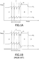
- Figures 1A and 1B show conventionally simulated band structure diagrams for a portion of an In x Al y Ga 1-x-y N light-emitting device including an n-type GaN layer 2 formed over a substrate (not shown), an active region 4 (including barrier layers 6 and quantum well layers 8), a p-type Al 0.2 Ga 0.8 N electron confinement layer 10, and a p-type GaN contact layer 12.
- the various layers illustrated are of wurtzite crystal structure with the c-axis of the crystal substantially perpendicular to the layers and directed from layer 2 toward layer 12. The simulations assume that the light-emitting device is driven at a forward current density of about 200 Amps / centimeter 2 (A/cm 2 ).
- the horizontal axes in Figures 1A and 1B represent position in the device in a direction perpendicular to the layers. The interfaces between the layers are indicated by dashed lines.
- the vertical axes in Figures 1A and 1B represent the energy of the conduction band edge E c and of the valence band edge E v in the various layers.
- the simulated band structure accounts for spontaneous and piezoelectric polarization fields in p-type Al y Ga 1-y N electron confinement layer 10 as well as for polarization fields in layer 2 and in active region 4.
- this simulation includes a negative sheet charge located at the interface of electron confinement layer 10 and active region 4, and a positive sheet charge located at the interface between confinement layer 10 and contact layer 12.
- FIG. 1B A comparison of Figures 1A and 1B shows that the effect of the sheet charges around Al y Ga 1-y N electron confinement layer 10 in Figure 1B is to reduce the magnitude of the potential energy barrier 14 that inhibits electrons from diffusing out of active region 4 into electron confinement layer 10.
- This reduction in electron confinement due to the polarization field in electron confinement layer 10 causes the quantum efficiency (ratio of photons out to electrons in) of the prior art device illustrated in Figure 1B to be lower than the quantum efficiency of the hypothetical device (having no polarization field in layer 10) illustrated in Figure 1A , particularly at high drive current densities.
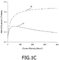
- FIG. 1C The difference in quantum efficiencies between the two devices is apparent in Figure 1C , in which the quantum efficiency 16 of the prior art device of Figure 1B and the quantum efficiency 18 of the hypothetical device of Figure 1A are plotted as a function of forward drive current density. These quantum efficiencies were simulated by conventional techniques. As Figure 1C indicates, at a forward current density of about 400 A/cm 2 the hypothetical device of Figure 1A in which electron barrier layer 10 has no polarization field is three times as efficient as the prior art device of Figure 1B in which electron barrier layer 10 is polarized.
- the drop in quantum efficiency of the prior art device shown in Figure 1B at high drive current densities must be primarily due to the reduction in height of potential barrier 14 by the polarization field in electron confinement layer 10.
- the inventors believe that, in contrast to the effects of polarization fields in the active region, the decrease in electron confinement and hence in quantum efficiency due to the polarization field in the electron confinement layer has not been previously recognized.
- polarization fields in n-type hole confinement layers may similarly reduce hole confinement and hence quantum efficiency. The inventors believe that the latter problem also has gone unrecognized.
- US 2003/085409 A1 discloses a III-nitride light emitting device and US 651513 B1 discloses an optical emitter with an active region sandwiched between cladding layers, with the active region and the cladding layers between n-type and p-type contact layers.
- III-Nitride light-emitting device having improved confinement of electrons and holes to its active region.
- the light-emitting semiconductor device comprises a III-Nitride active region and a III-Nitride layer formed proximate to the active region and may have a thickness that exceeds a critical thickness for relaxation of strain in the III-Nitride layer.
- the III-Nitride layer may be a carrier confinement layer, for example.
- the piezoelectric polarization in the III-Nitride layer may be reduced as a consequence of its thickness. The reduced polarization may result in an advantageous increase in the efficiency with which the device emits light.
- a light-emitting semiconductor device comprises a III-Nitride light emitting layer, an In x Al y Ga 1-x-y N (0.115 ⁇ x ⁇ 0.15, 0.2 ⁇ y ⁇ 0.35, x + y ⁇ 1), and a spacer layer interposing the light emitting layer and the In x Al y Ga 1-x-y N layer.
- the spacer layer is formed of GaN, InGaN or AlGaN.
- the spacer layer may advantageously space the In x Al y Ga 1-x-y N layer and any contaminants therein apart from the light emitting layer.
- the composition of the III-Nitride layer may be advantageously selected to determine a strength of an electric field in the III-Nitride layer and thereby increase the efficiency with which the device emits light.
- III-Nitride light-emitting devices Several embodiments are disclosed in which polarization fields are reduced in electron and/or hole confinement layers in III-Nitride light-emitting devices. Confinement of electrons and holes in the active regions of these devices may thereby be improved. This can result in devices with improved quantum efficiency.
- the III-Nitride light-emitting devices described may be, for example, light-emitting diodes or laser diodes.
- a III-N based LED 20 includes a sapphire substrate 22, a nucleation layer 24, an optional n-type III-Nitride contact layer, an n-type III-Nitride hole confinement layer 26, a III-Nitride active region 28, a p-type III-Nitride electron confinement layer 30, and an optional p-type III-Nitride contact layer 32.
- Active region 28 includes one or more quantum well layers and one or more barrier layers. Active region 28 may be spaced apart from electron confinement layer 30, hole confinement layer 26, or both by optional spacer layers 27 and 29.
- N-type ohmic electrode 34 may be disposed on n-type contact layer 23 or n-type hole confinement layer 26.
- P-type ohmic electrode 36 may be disposed on p-type contact layer 32 or p-type electron confinement layer 30. Application of a suitable forward bias across ohmic electrodes 34 and 36 results in emission of light from active region 28.
- the various semiconductor layers in light-emitting device 20 may be deposited by, for example, conventional metal-organic chemical vapor deposition (MOCVD) techniques.
- MOCVD metal-organic chemical vapor deposition
- Conventional photolithographic, etching, and deposition techniques may be used to form electrodes 34 and 36.
- the inventors have recognized that the piezoelectric polarization in electron confinement layer 30 can be advantageously reduced by growing this layer to a thickness exceeding its critical thickness for relaxation.
- the critical thickness is the thickness beyond which sufficient dislocations form in electron confinement layer 30 to substantially relax the strain induced in it by the difference in lattice dimensions between it and the layers underneath it.
- a layer that is thicker than its critical thickness is typically referred to in the art as a "relaxed layer.”
- electron confinement layer 30 is grown to a thickness beyond its critical thickness and is consequently a relaxed layer.
- the magnitude of the sheet charges at either side of electron confinement layer 30 is reduced to that caused by the spontaneous polarization alone.
- the resulting magnitude is generally about half of the value that includes the effect of strain (i.e., the piezoelectric polarization).
- each layer other than electron confinement layer 30 is grown to a thickness less than its critical thickness.
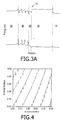
- the simulated band structure shown in Figure 3A accounts for the polarization fields in all of the layers shown and assumes that the light-emitting device is driven at a forward current density of about 200 A/cm 2 .
- the magnitude of the sheet charge on either side of electron confinement layer 30 has been reduced to the value due to spontaneous polarization alone. Consequently, electron confinement layer 30 in this implementation provides a larger potential barrier 14 to diffusion of electrons out of the active region than is provided by the strained prior art electron confinement layer 10 shown in Figure 1B .
- hole confinement layer 26 is grown to a thickness beyond its critical thickness and is therefore a relaxed layer. In such implementations, the magnitude of the sheet charges at either side of hole confinement layer 26 is reduced to that caused by the spontaneous polarization alone. Consequently, the confinement of holes to the active region is advantageously improved compared to prior art devices not utilizing relaxed III-Nitride hole confinement layers.
- Some implementations may include both a relaxed hole confinement layer 26 and a relaxed electron confinement layer 30.
- one of ordinary skill in the art typically avoids growing any layer near the active region in a III-Nitride light-emitting device to a thickness beyond the layer's critical thickness, as the resulting dislocations are generally expected to reduce the quantum efficiency of the device by forming nonradiative recombination centers for electrons and holes injected into the device. Also, as reported by Hiroki et al. and Shen et al., the electron mobility in or near layers that are relaxed tends to be much lower. The inventors have recognized that despite the possibility of nonradiative recombination at dislocations, the use of a relaxed confinement layer in a III-Nitride light-emitting device may be advantageous.
- the inventors have also recognized that the polarization fields in electron confinement layer 30 and/or in hole confinement layer 26 may be advantageously reduced, eliminated, or changed in sign by forming these layers from quaternary In x Al y Ga 1-x-y N alloys of particular compositions rather than from Al y Ga 1-y N alloys as used in the prior art.
- Quaternary In x Al y Ga 1-x-y N alloys include all three of In, Al, and Ga.
- An additional advantage to the use of quaternary In x Al y Ga 1-x-y N confinement layers is that they may be lattice-matched to GaN layers such as, for example, GaN barrier layers in the active region. Such lattice matching facilitates the formation of nitride semiconductor layers of improved crystallinity.
- Figure 4 illustrates the magnitude, in units of megavolts / centimeter (MV/cm), of the total polarization field (piezoelectric polarization + spontaneous polarization) across a layer of quaternary In x Al y Ga 1-x-y N grown on GaN.
- MV/cm total polarization field
- On the vertical axis is the mole fraction of aluminum in the layer, and on the horizontal axis is the mole fraction of indium in the layer.
- the lines with numbers in them are isometric lines of field magnitude.
- the case of the zero indium mole fraction i.e., the case of Al y Ga 1-y N).
- the height of the potential barrier to carrier diffusion provided by an In x Al y Ga 1-x-y N confinement layer is affected by both the net polarization in the layer and the bandgap of the In x Al y Ga 1-x-y N material, which decreases with increasing indium mole fraction.
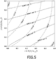
- Figure 5 shows the variation with composition of the energy gap of an In x Al y Ga 1-x-y N confinement layer grown on a GaN layer, and the variation with composition of the net polarization in the In x Al y Ga 1-x-y N confinement layer.
- the net polarization in each layer is the sum of the spontaneous polarization and the piezoelectric polarization.
- a difference in net polarization between two layers results in a sheet charge at the interface between the two layers. The larger the difference in net polarization, the larger the sheet charge.
- electron confinement layer 30 ( Figure 2 ) is formed from a quaternary In x Al y Ga 1-x-y N alloy having a mole fraction of indium selected to determine the strength of the polarization field in the layer and thereby increase the potential barrier 14 to electron diffusion provided by the layer.
- the sheet charges at either side of electron confinement layer 30 may be eliminated, reduced in magnitude, or changed in sign.
- the confinement of electrons to active region 28 and the quantum efficiency of light-emitting device 20 may be thereby improved.
- Suitable indium and aluminum mole fractions include to those in the range of 0.115 - 0.15and 0.2 - 0.35, respectively.
- compositions of the quaternary In x Al y Ga 1-x-y N confinement layer are determined by maximizing the confinement potential.
- the confinement potential is increased by a reduction in the sheet charge, and by an increase in the energy gap.
- Compositions of In x Al y Ga 1-x-y N which are advantageous for use as electron confinement layers are any of those compositions which have an energy gap greater than approximately 3.5 eV.
- the composition of the In x Al y Ga 1-x-y N electron confinement layer may be selected such that the difference between the net polarization in the electron confinement layer and the net polarization in an adjacent layer (a quantum well of the active region or spacer layer disposed between the electron confinement layer and the active region) is less than about 0.02 C/cm 2 , more preferably less than about 0.01 C/cm 2 .
- a quaternary In x Al y Ga 1-x-y N confinement layer with any amount of indium will be advantageous.
- the band structure of this implementation is illustrated in Figure 6A .
- Figure 6B the quantum efficiency of the novel device 60 illustrated in Figure 6A and the quantum efficiency 16 of the prior art device illustrated in Figure 1B are plotted as a function of forward drive current density. These quantum efficiencies were simulated by conventional techniques.
- the effect of the small energy gap of this layer on the confinement potential is offset by the effect of the small polarization sheet charge.
- the band structure of this implementation is illustrated in Figure 7A .
- hole confinement layer 26 ( Figure 2 ) is formed from a quaternary In x Al y Ga 1-x-y N alloy having a mole fraction of indium selected to determine the strength of the polarization field in the layer and thereby increase the potential barrier to hole diffusion provided by the layer.
- the sheet charges at either side of electron confinement layer 26 may be eliminated, reduced in magnitude, or changed in sign.
- the confinement of holes to active region 28 and the quantum efficiency of light-emitting device 20 may be thereby improved. It is particularly important for a hole confinement layer that the polarization sheet charge be small.
- the optimal composition of a quaternary In x Al y Ga 1-x-y N hole confinement layer is one with an energy gap greater than 3.5 eV, and one where the difference between the net polarization in the hole confinement layer and the net polarization in an adjacent layer is less than 0.02 C/cm 2 , more preferably less than about 0.01 C/cm 2 .
- the aluminum in quaternary III-Nitride confinement layers may promote contamination of these layers with oxygen. Such oxygen contaminants may enhance nonradiative recombination of electrons and holes in the quaternary III-Nitride layers and thereby reduce the quantum efficiency of a light-emitting device in which they are included.
- Such spacing apart is accomplished, for example, with spacer layers 27, 29 included in the active region. Spacer layers 27 and 29 may have a thickness between about 50 angstroms and about 200 angstroms. A common thickness is about 100 angstroms.
- Spacer layers 27 and 29 are usually n-type layers, though in some embodiments spacer layer 29 may be p-type.
- the spacer layers are GaN or ternary nitride alloys of aluminum, indium, and gallium.
- a GaN spacer layer 29 is disposed between electron confinement layer 30 and the quantum well layers 28.
- a GaN spacer layer 29 is disposed between electron confinement layer 30 and the quantum well layers 28.
- quaternary III-Nitride confinement layers may be in contact with light-emitting layers.
- Fig. 8 is a plan view of a large junction device (i.e. an area greater than or equal to 0.2 square millimeters).
- Fig. 9 is a cross section of the device shown in Fig. 8 , taken along axis DD.
- Figs. 8 and 9 illustrate an arrangement of contacts that may be used with any of the epitaxial structures 40 illustrated in Figs. 2 , 3A , 6A , 7A , and described above.
- the active region of epitaxial structure 40 is separated into four regions separated by three trenches in which n-contacts 34 are formed. Each region is connected to a submount by four p-submount connections 44 formed on p-contact 36.
- N-contact 34 surrounds the four active regions.
- N-contact 34 is connected to a submount by six n-submount connections 46.
- the n- and p-contacts may be electrically isolated by an insulating layer 42.
- Fig. 10 is an exploded view of a packaged light emitting device.
- a heat-sinking slug 100 is placed into an insert-molded leadframe.
- the insert-molded leadframe is, for example, a filled plastic material 105 molded around a metal frame 106 that provides an electrical path.
- Slug 100 may include an optional reflector cup 102.
- the light emitting device die 104 which may be any of the devices described above, is mounted directly or indirectly via a thermally conducting submount 103 to slug 100.
- a cover 108 which may be an optical lens, may be added.
- substrate 22 may be formed from materials other than sapphire, such as SiC.
- Electrode 36 may be transparent or semitransparent to light emitted by active region 28.
- electrode 36 may be highly reflective to light emitted by active region 28, and light-emitting device 20 may be mounted as a flip-chip with contacts 34 and 36 facing a submount.
- III-Nitride electron and hole confinement layers having reduced polarization fields as disclosed herein may be formed in other III-Nitride light-emitting devices such as, for example, those described in U. S. Patent 6,133,589 and in U.S. Patent 6,486,499 , both of which are assigned to the assignee of the present invention.
- light-emitting devices in accordance with the present invention may include layers not shown in the illustrated embodiments and may omit illustrated layers such as contact layer 32 ( Figure 2 ), for example.
- the composition of the various III-Nitride layers in the inventive light-emitting devices (such as the contact, quantum well, and barrier layers, for example) may vary from the example compositions disclosed.
Landscapes
- Engineering & Computer Science (AREA)
- Manufacturing & Machinery (AREA)
- Computer Hardware Design (AREA)
- Microelectronics & Electronic Packaging (AREA)
- Power Engineering (AREA)
- Led Devices (AREA)
- Led Device Packages (AREA)
Claims (12)
- Dispositif semi-conducteur électroluminescent (20) comprenant :- une région active de nitrure III (28) comprenant un certain nombre de couches électroluminescentes ;- une couche de confinement de nitrure III (26, 30) comprenant une couche de InxAlyGa1-x-yN, où 0,115 ≤ x ≤ 0,15, 0,2 ≤ y ≤ 0,35, et x + y ≤ 1 ; et- une couche d'espacement (27, 29) intercalée entre la région active (28) et une couche de confinement (26, 30),dans lequel la couche d'espacement est formée de GaN, InGaN ou AlGaN.
- Dispositif semi-conducteur électroluminescent selon la revendication 1, dans lequel une couche de confinement (26, 30) est en contact direct avec une couche d'espacement (27, 29).
- Dispositif semi-conducteur électroluminescent selon l'une quelconque des revendications précédentes, dans lequel une couche de confinement (26, 30) est de conductivité de type p.
- Dispositif semi-conducteur électroluminescent selon l'une quelconque des revendications précédentes, dans lequel une couche de confinement (26, 30) est de conductivité de type n.
- Dispositif semi-conducteur électroluminescent selon l'une quelconque des revendications précédentes, dans lequel une couche de confinement (26, 30) a une bande interdite supérieure à environ 3,5 eV.
- Dispositif semi-conducteur électroluminescent selon la revendication 1, dans lequel la composition d'indium x et la composition d'aluminium y d'une couche de confinement (26, 30) sont choisies de sorte qu'une différence entre une polarisation nette dans la couche de confinement (26, 30) et une polarisation nette dans une couche d'espacement (27, 29) a une magnitude inférieure à environ 0,02 C/m2.
- Dispositif semi-conducteur électroluminescent selon la revendication 1, dans lequel la composition d'indium x et la composition d'aluminium y d'une couche de confinement (26, 30) sont choisies de sorte qu'une différence entre une polarisation nette dans la couche de confinement (26, 30) et une polarisation nette dans une couche d'espacement (27, 29) a une magnitude inférieure à environ 0,01 C/m2.
- Dispositif semi-conducteur électroluminescent selon l'une quelconque des revendications précédentes, dans lequel la région active (28) est disposée entre une région de type n et une région de type p, le dispositif comprenant en outre :- des premier et second contacts (23, 32) disposés sur les régions de types p et n ;- des premier et second fils électriquement couplés aux premier et second contacts (23, 32) ; et- un revêtement disposé sur la couche électroluminescente.
- Dispositif semi-conducteur électroluminescent selon l'une quelconque des revendications précédentes, dans lequel une épaisseur d'une couche de confinement (26, 30) excède environ 400 Angströms.
- Dispositif semi-conducteur électroluminescent selon l'une quelconque des revendications précédentes, dans lequel une épaisseur d'une couche de confinement (26, 30) excède environ 700 Angströms.
- Dispositif semi-conducteur électroluminescent selon l'une quelconque des revendications précédentes, dans lequel une épaisseur d'une couche de confinement (26, 30) excède environ 900 Angströms.
- Dispositif semi-conducteur électroluminescent selon l'une quelconque des revendications précédentes, dans lequel la couche d'espacement (27, 29) a une épaisseur comprise entre 50 et 200 Angströms.
Applications Claiming Priority (2)
| Application Number | Priority Date | Filing Date | Title |
|---|---|---|---|
| US10/769,590 US6943381B2 (en) | 2004-01-30 | 2004-01-30 | III-nitride light-emitting devices with improved high-current efficiency |
| US769590 | 2004-01-30 |
Publications (3)
| Publication Number | Publication Date |
|---|---|
| EP1560277A2 EP1560277A2 (fr) | 2005-08-03 |
| EP1560277A3 EP1560277A3 (fr) | 2006-08-02 |
| EP1560277B1 true EP1560277B1 (fr) | 2019-04-03 |
Family
ID=34654392
Family Applications (1)
| Application Number | Title | Priority Date | Filing Date |
|---|---|---|---|
| EP05100422.4A Active EP1560277B1 (fr) | 2004-01-30 | 2005-01-24 | Dispositifs émettants de lumière fabriqués de matériau III-nitrure plus efficace aux courants forts |
Country Status (4)
| Country | Link |
|---|---|
| US (1) | US6943381B2 (fr) |
| EP (1) | EP1560277B1 (fr) |
| JP (1) | JP2005217421A (fr) |
| TW (1) | TWI374551B (fr) |
Families Citing this family (39)
| Publication number | Priority date | Publication date | Assignee | Title |
|---|---|---|---|---|
| US7692182B2 (en) * | 2001-05-30 | 2010-04-06 | Cree, Inc. | Group III nitride based quantum well light emitting device structures with an indium containing capping structure |
| US6958497B2 (en) | 2001-05-30 | 2005-10-25 | Cree, Inc. | Group III nitride based light emitting diode structures with a quantum well and superlattice, group III nitride based quantum well structures and group III nitride based superlattice structures |
| TWI244221B (en) * | 2004-03-01 | 2005-11-21 | Epistar Corp | Micro-reflector containing flip-chip light emitting device |
| FI20041213A0 (fi) * | 2004-09-17 | 2004-09-17 | Optogan Oy | Puolijohdeheterorakenne |
| US7221000B2 (en) * | 2005-02-18 | 2007-05-22 | Philips Lumileds Lighting Company, Llc | Reverse polarization light emitting region for a semiconductor light emitting device |
| US20070045638A1 (en) | 2005-08-24 | 2007-03-01 | Lumileds Lighting U.S., Llc | III-nitride light emitting device with double heterostructure light emitting region |
| JP2009530798A (ja) | 2006-01-05 | 2009-08-27 | イルミテックス, インコーポレイテッド | Ledから光を導くための独立した光学デバイス |
| US7789531B2 (en) | 2006-10-02 | 2010-09-07 | Illumitex, Inc. | LED system and method |
| US7834367B2 (en) | 2007-01-19 | 2010-11-16 | Cree, Inc. | Low voltage diode with reduced parasitic resistance and method for fabricating |
| US20080197378A1 (en) * | 2007-02-20 | 2008-08-21 | Hua-Shuang Kong | Group III Nitride Diodes on Low Index Carrier Substrates |
| US20090050875A1 (en) | 2007-08-20 | 2009-02-26 | Samsung Electro-Mechanics Co., Ltd. | Nitride semiconductor light emitting device |
| US8546846B2 (en) | 2007-08-20 | 2013-10-01 | Samsung Electronics Co., Ltd. | Nitride semiconductor light emitting device |
| US9012937B2 (en) | 2007-10-10 | 2015-04-21 | Cree, Inc. | Multiple conversion material light emitting diode package and method of fabricating same |
| EP2240968A1 (fr) | 2008-02-08 | 2010-10-20 | Illumitex, Inc. | Systeme et procede de mise en forme de la couche emettrice |
| KR101142672B1 (ko) | 2008-09-11 | 2012-05-11 | 스미토모덴키고교가부시키가이샤 | 질화물계 반도체 광소자, 질화물계 반도체 광소자용의 에피택셜 웨이퍼, 및 반도체 발광 소자를 제조하는 방법 |
| TW201034256A (en) | 2008-12-11 | 2010-09-16 | Illumitex Inc | Systems and methods for packaging light-emitting diode devices |
| US8227791B2 (en) * | 2009-01-23 | 2012-07-24 | Invenlux Limited | Strain balanced light emitting devices |
| US8449128B2 (en) | 2009-08-20 | 2013-05-28 | Illumitex, Inc. | System and method for a lens and phosphor layer |
| US8585253B2 (en) | 2009-08-20 | 2013-11-19 | Illumitex, Inc. | System and method for color mixing lens array |
| US9293644B2 (en) | 2009-09-18 | 2016-03-22 | Soraa, Inc. | Power light emitting diode and method with uniform current density operation |
| US9583678B2 (en) | 2009-09-18 | 2017-02-28 | Soraa, Inc. | High-performance LED fabrication |
| US8933644B2 (en) | 2009-09-18 | 2015-01-13 | Soraa, Inc. | LED lamps with improved quality of light |
| KR101368906B1 (ko) * | 2009-09-18 | 2014-02-28 | 소라, 인코포레이티드 | 전력 발광 다이오드 및 전류 밀도 작동 방법 |
| WO2011058697A1 (fr) * | 2009-11-12 | 2011-05-19 | パナソニック株式会社 | Procédé de fabrication d'un élément semi-conducteur à base de nitrure |
| US8604461B2 (en) | 2009-12-16 | 2013-12-10 | Cree, Inc. | Semiconductor device structures with modulated doping and related methods |
| US8536615B1 (en) | 2009-12-16 | 2013-09-17 | Cree, Inc. | Semiconductor device structures with modulated and delta doping and related methods |
| US8993996B2 (en) | 2010-01-08 | 2015-03-31 | Sensor Electronic Technology, Inc. | Superlattice structure |
| US8895959B2 (en) | 2010-01-08 | 2014-11-25 | Sensor Electronic Technology, Inc. | Superlattice structure and method for making the same |
| US9412901B2 (en) | 2010-01-08 | 2016-08-09 | Sensor Electronic Technology, Inc. | Superlattice structure |
| US8698127B2 (en) * | 2010-01-08 | 2014-04-15 | Sensor Electronic Technology, Inc. | Superlattice structure and method for making the same |
| US9768349B2 (en) | 2010-01-08 | 2017-09-19 | Sensor Electronic Technology, Inc. | Superlattice structure |
| CN102136536A (zh) | 2010-01-25 | 2011-07-27 | 亚威朗(美国) | 应变平衡发光器件 |
| US8575592B2 (en) * | 2010-02-03 | 2013-11-05 | Cree, Inc. | Group III nitride based light emitting diode structures with multiple quantum well structures having varying well thicknesses |
| WO2012157198A1 (fr) | 2011-05-18 | 2012-11-22 | パナソニック株式会社 | Élément électroluminescent à semi-conducteur nitrure et son procédé de fabrication |
| KR101910564B1 (ko) * | 2011-06-02 | 2018-10-22 | 서울바이오시스 주식회사 | 스트레인 강화된 웰층을 갖는 발광 다이오드 |
| CN103378121A (zh) * | 2012-04-27 | 2013-10-30 | 华夏光股份有限公司 | 发光二极管装置 |
| CN104350651B (zh) | 2012-05-22 | 2017-08-01 | 松下知识产权经营株式会社 | 氮化物半导体发光装置 |
| US9761763B2 (en) | 2012-12-21 | 2017-09-12 | Soraa, Inc. | Dense-luminescent-materials-coated violet LEDs |
| US9410664B2 (en) | 2013-08-29 | 2016-08-09 | Soraa, Inc. | Circadian friendly LED light source |
Citations (1)
| Publication number | Priority date | Publication date | Assignee | Title |
|---|---|---|---|---|
| US20030085409A1 (en) * | 2001-11-02 | 2003-05-08 | Yu-Chen Shen | Indium gallium nitride separate confinement heterostructure light emitting devices |
Family Cites Families (14)
| Publication number | Priority date | Publication date | Assignee | Title |
|---|---|---|---|---|
| US58349A (en) * | 1866-09-25 | Improvement in corn-harvesters | ||
| JPH10150245A (ja) * | 1996-11-21 | 1998-06-02 | Matsushita Electric Ind Co Ltd | 窒化ガリウム系半導体の製造方法 |
| JP2950799B2 (ja) * | 1997-08-26 | 1999-09-20 | 株式会社東芝 | 非線形光デバイス |
| US6849472B2 (en) * | 1997-09-30 | 2005-02-01 | Lumileds Lighting U.S., Llc | Nitride semiconductor device with reduced polarization fields |
| JP3577206B2 (ja) * | 1997-12-04 | 2004-10-13 | 昭和電工株式会社 | Iii族窒化物半導体発光素子 |
| US6194742B1 (en) * | 1998-06-05 | 2001-02-27 | Lumileds Lighting, U.S., Llc | Strain engineered and impurity controlled III-V nitride semiconductor films and optoelectronic devices |
| US6133589A (en) * | 1999-06-08 | 2000-10-17 | Lumileds Lighting, U.S., Llc | AlGaInN-based LED having thick epitaxial layer for improved light extraction |
| US6515313B1 (en) * | 1999-12-02 | 2003-02-04 | Cree Lighting Company | High efficiency light emitters with reduced polarization-induced charges |
| US6764888B2 (en) | 2000-09-27 | 2004-07-20 | Sensor Electronic Technology, Inc. | Method of producing nitride-based heterostructure devices |
| US6576932B2 (en) * | 2001-03-01 | 2003-06-10 | Lumileds Lighting, U.S., Llc | Increasing the brightness of III-nitride light emitting devices |
| WO2003041234A1 (fr) * | 2001-11-05 | 2003-05-15 | Nichia Corporation | Element semi-conducteur |
| US6683327B2 (en) * | 2001-11-13 | 2004-01-27 | Lumileds Lighting U.S., Llc | Nucleation layer for improved light extraction from light emitting devices |
| US20030230977A1 (en) * | 2002-06-12 | 2003-12-18 | Epstein Howard C. | Semiconductor light emitting device with fluoropolymer lens |
| JP2004214698A (ja) * | 2004-03-29 | 2004-07-29 | Nichia Chem Ind Ltd | 窒化物半導体発光素子 |
-
2004
- 2004-01-30 US US10/769,590 patent/US6943381B2/en not_active Expired - Lifetime
-
2005
- 2005-01-24 EP EP05100422.4A patent/EP1560277B1/fr active Active
- 2005-01-27 TW TW094102474A patent/TWI374551B/zh active
- 2005-01-28 JP JP2005021485A patent/JP2005217421A/ja active Pending
Patent Citations (1)
| Publication number | Priority date | Publication date | Assignee | Title |
|---|---|---|---|---|
| US20030085409A1 (en) * | 2001-11-02 | 2003-05-08 | Yu-Chen Shen | Indium gallium nitride separate confinement heterostructure light emitting devices |
Also Published As
| Publication number | Publication date |
|---|---|
| EP1560277A3 (fr) | 2006-08-02 |
| TW200536149A (en) | 2005-11-01 |
| US20050167690A1 (en) | 2005-08-04 |
| JP2005217421A (ja) | 2005-08-11 |
| US6943381B2 (en) | 2005-09-13 |
| EP1560277A2 (fr) | 2005-08-03 |
| TWI374551B (en) | 2012-10-11 |
Similar Documents
| Publication | Publication Date | Title |
|---|---|---|
| EP1560277B1 (fr) | Dispositifs émettants de lumière fabriqués de matériau III-nitrure plus efficace aux courants forts | |
| US7115908B2 (en) | III-nitride light emitting device with reduced polarization fields | |
| US6995389B2 (en) | Heterostructures for III-nitride light emitting devices | |
| KR100267839B1 (ko) | 질화물 반도체 장치 | |
| US6515313B1 (en) | High efficiency light emitters with reduced polarization-induced charges | |
| US7737451B2 (en) | High efficiency LED with tunnel junction layer | |
| EP1653522B1 (fr) | Dispositif semiconducteur émetteur de lumière avec couches à gradient de composition | |
| EP1589593B1 (fr) | Dispositif électroluminescent en nitrures du groupe III contrôlé par contrainte | |
| US7939833B2 (en) | Nitride semiconductor light emitting device | |
| US7221000B2 (en) | Reverse polarization light emitting region for a semiconductor light emitting device | |
| US10304997B2 (en) | III-nitride light emitting device with a region including only ternary, quaternary, and/or quinary III-nitride layers | |
| US20040077135A1 (en) | Light-emitting diode device geometry | |
| US20060244002A1 (en) | A semiconductor light-emitting device, and a method of manufacture of a semiconductor device | |
| WO2000021144A9 (fr) | DIODE ELECTROLUMINESCENTE InGaN A GEOMETRIE VERTICALE | |
| JP2010532926A (ja) | 放射線放出半導体ボディ | |
| US7285799B2 (en) | Semiconductor light emitting devices including in-plane light emitting layers | |
| JP2001185757A (ja) | Iii族窒化物系化合物半導体発光素子 |
Legal Events
| Date | Code | Title | Description |
|---|---|---|---|
| PUAI | Public reference made under article 153(3) epc to a published international application that has entered the european phase |
Free format text: ORIGINAL CODE: 0009012 |
|
| AK | Designated contracting states |
Kind code of ref document: A2 Designated state(s): AT BE BG CH CY CZ DE DK EE ES FI FR GB GR HU IE IS IT LI LT LU MC NL PL PT RO SE SI SK TR |
|
| AX | Request for extension of the european patent |
Extension state: AL BA HR LV MK YU |
|
| PUAL | Search report despatched |
Free format text: ORIGINAL CODE: 0009013 |
|
| AK | Designated contracting states |
Kind code of ref document: A3 Designated state(s): AT BE BG CH CY CZ DE DK EE ES FI FR GB GR HU IE IS IT LI LT LU MC NL PL PT RO SE SI SK TR |
|
| AX | Request for extension of the european patent |
Extension state: AL BA HR LV MK YU |
|
| 17P | Request for examination filed |
Effective date: 20070202 |
|
| AKX | Designation fees paid |
Designated state(s): DE |
|
| RAP1 | Party data changed (applicant data changed or rights of an application transferred) |
Owner name: PHILIPS LUMILEDS LIGHTING COMPANY LLC |
|
| 17Q | First examination report despatched |
Effective date: 20160705 |
|
| RAP1 | Party data changed (applicant data changed or rights of an application transferred) |
Owner name: LUMILEDS HOLDING B.V. |
|
| GRAP | Despatch of communication of intention to grant a patent |
Free format text: ORIGINAL CODE: EPIDOSNIGR1 |
|
| INTG | Intention to grant announced |
Effective date: 20181205 |
|
| RIC1 | Information provided on ipc code assigned before grant |
Ipc: H01L 33/00 20100101AFI20050607BHEP |
|
| GRAS | Grant fee paid |
Free format text: ORIGINAL CODE: EPIDOSNIGR3 |
|
| RAP1 | Party data changed (applicant data changed or rights of an application transferred) |
Owner name: LUMILEDS HOLDING B.V. |
|
| GRAA | (expected) grant |
Free format text: ORIGINAL CODE: 0009210 |
|
| AK | Designated contracting states |
Kind code of ref document: B1 Designated state(s): DE |
|
| REG | Reference to a national code |
Ref country code: DE Ref legal event code: R096 Ref document number: 602005055584 Country of ref document: DE |
|
| REG | Reference to a national code |
Ref country code: DE Ref legal event code: R097 Ref document number: 602005055584 Country of ref document: DE |
|
| PLBE | No opposition filed within time limit |
Free format text: ORIGINAL CODE: 0009261 |
|
| STAA | Information on the status of an ep patent application or granted ep patent |
Free format text: STATUS: NO OPPOSITION FILED WITHIN TIME LIMIT |
|
| 26N | No opposition filed |
Effective date: 20200106 |
|
| P01 | Opt-out of the competence of the unified patent court (upc) registered |
Effective date: 20230530 |
|
| PGFP | Annual fee paid to national office [announced via postgrant information from national office to epo] |
Ref country code: DE Payment date: 20240129 Year of fee payment: 20 |