EP1560033A1 - Integrated circuit comprising a secure test mode by resetting of said test mode - Google Patents
Integrated circuit comprising a secure test mode by resetting of said test mode Download PDFInfo
- Publication number
- EP1560033A1 EP1560033A1 EP05366001A EP05366001A EP1560033A1 EP 1560033 A1 EP1560033 A1 EP 1560033A1 EP 05366001 A EP05366001 A EP 05366001A EP 05366001 A EP05366001 A EP 05366001A EP 1560033 A1 EP1560033 A1 EP 1560033A1
- Authority
- EP
- European Patent Office
- Prior art keywords
- circuit
- cells
- test
- initialization
- configurable cells
- Prior art date
- Legal status (The legal status is an assumption and is not a legal conclusion. Google has not performed a legal analysis and makes no representation as to the accuracy of the status listed.)
- Withdrawn
Links
Images

Classifications
-
- G—PHYSICS
- G06—COMPUTING OR CALCULATING; COUNTING
- G06F—ELECTRIC DIGITAL DATA PROCESSING
- G06F21/00—Security arrangements for protecting computers, components thereof, programs or data against unauthorised activity
- G06F21/70—Protecting specific internal or peripheral components, in which the protection of a component leads to protection of the entire computer
- G06F21/71—Protecting specific internal or peripheral components, in which the protection of a component leads to protection of the entire computer to assure secure computing or processing of information
- G06F21/75—Protecting specific internal or peripheral components, in which the protection of a component leads to protection of the entire computer to assure secure computing or processing of information by inhibiting the analysis of circuitry or operation
-
- G—PHYSICS
- G01—MEASURING; TESTING
- G01R—MEASURING ELECTRIC VARIABLES; MEASURING MAGNETIC VARIABLES
- G01R31/00—Arrangements for testing electric properties; Arrangements for locating electric faults; Arrangements for electrical testing characterised by what is being tested not provided for elsewhere
- G01R31/28—Testing of electronic circuits, e.g. by signal tracer
- G01R31/317—Testing of digital circuits
- G01R31/31719—Security aspects, e.g. preventing unauthorised access during test
-
- G—PHYSICS
- G01—MEASURING; TESTING
- G01R—MEASURING ELECTRIC VARIABLES; MEASURING MAGNETIC VARIABLES
- G01R31/00—Arrangements for testing electric properties; Arrangements for locating electric faults; Arrangements for electrical testing characterised by what is being tested not provided for elsewhere
- G01R31/28—Testing of electronic circuits, e.g. by signal tracer
- G01R31/317—Testing of digital circuits
- G01R31/3181—Functional testing
- G01R31/3185—Reconfiguring for testing, e.g. LSSD, partitioning
- G01R31/318533—Reconfiguring for testing, e.g. LSSD, partitioning using scanning techniques, e.g. LSSD, Boundary Scan, JTAG
Definitions
- scanpath Such a technique of testing internal paths of a integrated circuit (referred to as “scanpath” or “internal scan method "in English language) is for example described in the publication by Williams and J. Angel, entitled “Enhancing Testability of LSI Circuits Via Test Points and Additional Logic, IEEE Transactions on Computers, flight. C-22, no.1; January 1973 ".
- each of the flip-flops of the circuit logic has at its entrance a multiplexer.
- the different flip-flops and multiplexers that are associated thus constitute so many cells Configurable whose accesses are individually controlled by these multiplexers.
- the multiplexers of these different cells Configurable are collectively controlled by a access controller or "TAP controller" ("TAP" for "Test Access Port "in English language) which is inactive or active according to a chosen mode of operation of the circuit electronic mode (standard operating mode or test).
- TAP controller When the TAP controller is activated by a signal mode control (switching to circuit test mode electronic) it uses this set of cells configurable as a standard functional circuit, integrated into the logic circuit that it forms with the cells logical, or as a test circuit.
- the TAP controller addresses on different control conductors, by which it is connected to different configurable cells, signals from command, such as a chaining command signal or still a data propagation control signal, that change the paths of data flow to within the integrated circuit and thus enabling the capture of these data by the controller, with a view to analysis.
- commands such as a chaining command signal or still a data propagation control signal
- the TAP controller is inactive and configurable cell multiplexers are positioned in such a way that the flip-flops of these cells are connected to logical cells surrounding areas to define one or more subsets functionalities of the integrated circuit.
- the TAP controller In the test mode of the electronic circuit, the TAP controller is normally activated by a command test execution received from the outside, and it can produce a chaining command signal to connect in series the flip-flops of the configurable cells of to form a shift register.
- This register includes in particular a serial input and a serial output respectively connected to an output and to a TAP controller input, as well as an input clock receiving a clock signal to clock the flow of data.
- a new test can possibly be executed. After completion of all the tests, the controller produces a signal indicating the end of the test mode (deactivation by the controller the test control signal).
- a fraudster may obtain information about secret data, or even reconstruct them.
- a fraudster may also write access to cell latches configurable to insert fraudulent data, or good for placing the integrated circuit in a unauthorized configuration. It will be able for example access a registry controlling a secure organ such as a sensor to disable it. He may also injecting erroneous data in order to obtain information on a secret data.
- the object of the invention is precisely to propose a electronic circuit designed to defeat this type of attempted fraud.
- the configurable cells are initialized. Stop the standard operation of the electronic circuit, pass in test mode and unload the contents of the latches do not allows more to obtain information about the contents of configurable cells at the instant of the interruption. Of the same way, if data are introduced into the configurable cells just before switching from the mode of standard mode test, this data is erased by a initialization before activating the standard mode. It is not therefore no longer possible to inject erroneous data.
- the verification of the state of the cells makes it possible in particular to check that initialization signals have been correctly sent, that there is no break in conductors on which these signals pass, etc.
- the circuit of validation includes a verification circuit that receives data output signals from the cells configurable and delivers an adopting status signal selectively a representative state of an initialization correct or a representative state of an initialization incorrect configurable cells, depending on whether output signals correspond or not to predefined output.
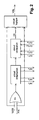
- the circuit of FIG. 1 comprises in particular a set configurable cells C1, ..., CN identical (only the NC cell is detailed) and a control circuit (or TAP controller), together forming a circuit identical to a known electronic circuit as described in preamble of the description.
- Each configurable cell includes a MUX multiplexer and a flip-flop B, for example Flip-Flop type.
- the circuit TAP produces the control signals MODE1, MODE2, ..., MODEN (from the same source), each signal coming respectively configure a cell C1, ..., CN, and more precisely the multiplexer MUX this cell.
- the MUX multiplexer connects a data entry from flip-flop B to an input of data E1 of the cell, said input E1 being functionally connected to one or more cells logical (not represented) with which the rocker cooperates to form a logic circuit.
- the MUX multiplexer connects the data input of flip-flop B to a data input E2 of the cell, the said input E2 being functionally connected to an output S of given from a previous cell. All N cells thus form a shift register. E2 entry of the first cell C1 forms the entry of the register to offset and the S output of the last CN cell form the output of the said register.
- test mode is activated (and in consequence the standard operating mode disabled) when the controller is activated by a signal from outside; and the test mode is disabled when the controller produces a signal indicating the end of the unloading data from cells configurable.
- the known circuit is completed by a validation circuit that will handle the beginning and the end a test mode.
- a validation circuit is shown in Figure 2.
- Each signal INIT1, ..., INITN comes initialize respectively a cell C1, ..., CN, and more precisely imposes an initial value on the flip-flop B of this cell.
- the validation circuit also includes a circuit of verification that receives a set of output signals OUT1, OUT2, ..., OUTN, respectively corresponding to output signals of cells C1, C2, ..., CN.
- the verification circuit is for example a combinational logic circuit, which combines the signals OUT1, ..., OUTN, or only a part of them, and delivers an OK output signal that is active or inactive depending on whether the combination of signals corresponds to an expected value.
- the signals OUT1, OUT2, OUTN are not not necessarily all equal to 1 or 0, but have always the same value after each initialization, so that at each initialization validly performed, the combination of signals OUT1, ..., OUTN always has the same expected value.
Landscapes
- Engineering & Computer Science (AREA)
- Physics & Mathematics (AREA)
- General Engineering & Computer Science (AREA)
- General Physics & Mathematics (AREA)
- Computer Hardware Design (AREA)
- Computer Security & Cryptography (AREA)
- Theoretical Computer Science (AREA)
- Mathematical Physics (AREA)
- Software Systems (AREA)
- Logic Circuits (AREA)
- Tests Of Electronic Circuits (AREA)
Abstract
Description
L'invention concerne, de façon générale, les circuits électroniques intégrés synchrones munis de moyens de logique combinatoire, de bascules, et de moyens de test. Plus précisément, l'invention concerne un circuit électronique comprenant une pluralité de cellules configurables et un circuit de commande, le dit circuit électronique étant adapté pour fonctionner dans un mode de fonctionnement standard ou dans un mode de test au cours duquel le circuit de commande est actif et configure les dites cellules configurables :
- soit dans un état fonctionnel dans lequel les cellules configurables sont fonctionnellement reliées à des cellules logiques avec lesquelles elles coopèrent pour former un circuit logique,
- soit dans un état chaíné dans lequel les cellules configurables sont fonctionnellement connectées en chaíne pour former un registre à décalage.
- in a functional state in which the configurable cells are functionally connected to logic cells with which they cooperate to form a logic circuit,
- in a chained state in which the configurable cells are functionally connected in a chain to form a shift register.
Il est aujourd'hui bien connu de tester le fonctionnement correct des éléments fonctionnels d'un circuit intégré en imposant et / ou en déterminant, à des instants prédéfinis, des valeurs de données présentes en certains points internes de ce circuit intégré.It is now well known to test the functioning correct functional elements of an integrated circuit in imposing and / or determining, at times predefined, data values present in some internal points of this integrated circuit.
Une telle technique de test de chemins internes d'un circuit intégré (désignée par "scanpath" ou "internal scan method" en langue anglaise) est par exemple décrite dans la publication de M. Williams et J. Angel, intitulée "Enhancing Testability of LSI Circuits Via Test Points and Additional Logic, IEEE Transactions on Computers, vol. C-22, no.1; Janvier 1973". Such a technique of testing internal paths of a integrated circuit (referred to as "scanpath" or "internal scan method "in English language) is for example described in the publication by Williams and J. Angel, entitled "Enhancing Testability of LSI Circuits Via Test Points and Additional Logic, IEEE Transactions on Computers, flight. C-22, no.1; January 1973 ".
Selon cette technique, chacune des bascules du circuit logique, dont il est utile de connaítre l'état et / ou d'imposer le contenu durant le fonctionnement standard du circuit intégré, est dotée à son entrée d'un multiplexeur.According to this technique, each of the flip-flops of the circuit logic, of which it is useful to know the state and / or to impose the content during the standard operation of the integrated circuit, has at its entrance a multiplexer.
Les différentes bascules et les multiplexeurs qui leur sont associés constituent ainsi autant de cellules configurables dont les accès sont individuellement contrôlés par ces multiplexeurs.The different flip-flops and multiplexers that are associated thus constitute so many cells Configurable whose accesses are individually controlled by these multiplexers.
Les multiplexeurs de ces différentes cellules configurables sont collectivement commandés par un contrôleur d'accès ou "contrôleur TAP" ("TAP" pour "Test Access Port" en langue anglaise) qui est inactif ou actif selon un mode de fonctionnement choisi du circuit électronique (mode de fonctionnement standard ou mode de test). Lorsque le contrôleur TAP est activé par un signal de commande de mode (passage en mode de test du circuit électronique), il utilise cet ensemble de cellules configurables soit comme un circuit fonctionnel standard, intégré au circuit logique qu'il forme avec les cellules logiques, soit comme un circuit de test.The multiplexers of these different cells Configurable are collectively controlled by a access controller or "TAP controller" ("TAP" for "Test Access Port "in English language) which is inactive or active according to a chosen mode of operation of the circuit electronic mode (standard operating mode or test). When the TAP controller is activated by a signal mode control (switching to circuit test mode electronic) it uses this set of cells configurable as a standard functional circuit, integrated into the logic circuit that it forms with the cells logical, or as a test circuit.
Pour ce faire, le contrôleur TAP adresse sur différents conducteurs de commande, par lesquels il est relié aux différentes cellules configurables, des signaux de commande, tels qu'un signal de commande de chaínage ou encore un signal de commande de propagation de données, qui modifient les chemins de circulation des données au sein du circuit intégré et qui permettent ainsi la capture de ces données par le contrôleur, en vue de leur analyse.To do this, the TAP controller addresses on different control conductors, by which it is connected to different configurable cells, signals from command, such as a chaining command signal or still a data propagation control signal, that change the paths of data flow to within the integrated circuit and thus enabling the capture of these data by the controller, with a view to analysis.
En mode de fonctionnement standard, le contrôleur TAP est inactif et les multiplexeurs des cellules configurables sont positionnés de manière telle que les bascules de ces cellules soient connectées à des cellules logiques environnantes pour définir un ou plusieurs sous-ensembles fonctionnels du circuit intégré.In standard operating mode, the TAP controller is inactive and configurable cell multiplexers are positioned in such a way that the flip-flops of these cells are connected to logical cells surrounding areas to define one or more subsets functionalities of the integrated circuit.
Dans le mode de test du circuit électronique, le contrôleur TAP est normalement activé par une commande d'exécution de test reçue de l'extérieur, et il peut produire un signal de commande de chaínage pour connecter en série les bascules des cellules configurables de manière à former un registre à décalage.In the test mode of the electronic circuit, the TAP controller is normally activated by a command test execution received from the outside, and it can produce a chaining command signal to connect in series the flip-flops of the configurable cells of to form a shift register.
Ce registre comporte notamment une entrée série et une sortie série respectivement connectées à une sortie et à une entrée du contrôleur TAP, ainsi qu'une entrée d'horloge recevant un signal d'horloge pour cadencer le flot de données.This register includes in particular a serial input and a serial output respectively connected to an output and to a TAP controller input, as well as an input clock receiving a clock signal to clock the flow of data.
Un test du circuit intégré est réalisé en activant le contrôleur TAP ; le test comprend principalement les trois étapes suivantes.
- Dans un premier temps, le contrôleur TAP configure les cellules en mode de test puis charge en série des données dans les bascules des cellules configurables par l'entrée du registre à décalage que forment ces cellules.
- Puis, le contrôleur TAP change la commutation des multiplexeurs pour former le circuit fonctionnel (mode de fonctionnement standard), et commande l'exécution d'un ou plusieurs cycles d'horloge par ce circuit fonctionnel. Les données chargées dans les bascules des cellules configurables sont alors traitées par le circuit fonctionnel.
- Le contrôleur change alors une nouvelle fois la commutation des multiplexeurs pour former à nouveau le registre à décalage (mode de test) et récupère, en série sur la sortie du registre à décalage, les données mémorisées dans les bascules des cellules configurables durant le dernier cycle d'horloge.
- Initially, the TAP controller configures the cells in test mode and then serially loads data into the flip-flops of the cells that can be configured by the input of the shift register that these cells form.
- Then, the TAP controller changes the switching of the multiplexers to form the functional circuit (standard operating mode), and controls the execution of one or more clock cycles by this functional circuit. The data loaded in the flip-flops of the configurable cells are then processed by the functional circuit.
- The controller then changes the switching of the multiplexers once again to form the shift register (test mode) and recovers, in series on the output of the shift register, the data stored in the latches of the configurable cells during the last cycle. clock.
Après déchargement complet des données, un nouveau test peut éventuellement être exécuté. Après réalisation de tous les test, le contrôleur produit un signal indiquant la fin du mode de test (désactivation par le contrôleur du signal de commande de test).After complete unloading of the data, a new test can possibly be executed. After completion of all the tests, the controller produces a signal indicating the end of the test mode (deactivation by the controller the test control signal).
En dépit de l'intérêt confirmé de cette technique de test, son application pratique peut en certaines circonstances s'avérer problématique, notamment sur les circuits intégrés qui traitent des données secrètes.Despite the confirmed interest of this technique of test, its practical application can in some circumstances prove to be problematic, in particular integrated circuits that process secret data.
En effet, dans la mesure où l'activation du mode de test peut permettre à un fraudeur de lire le contenu des bascules des cellules configurables, cette technique de test présente a priori l'inconvénient de rendre de tels circuits très vulnérables à une utilisation frauduleuse.Indeed, since the activation of the test mode may allow a fraudster to read the content of the flip-flops of configurable cells, this technique of test has the disadvantage of rendering such circuits very vulnerable to fraudulent use.
Par exemple, en stoppant à divers moments un processus de chargement interne de données secrètes dans le circuit intégré et en déchargeant le contenu du registre à décalage, un fraudeur pourra obtenir des informations sur des données secrètes, voire les reconstituer.For example, by stopping at various times a process of internal loading of secret data into the circuit integrated and unloading the contents of the register to offset, a fraudster may obtain information about secret data, or even reconstruct them.
En activant le mode de test, un fraudeur pourra également accéder en écriture aux bascules des cellules configurables pour insérer des données frauduleuses, ou bien pour placer le circuit intégré dans une configuration non autorisée. Il pourra ainsi par exemple accéder à un registre contrôlant un organe sécuritaire tel qu'un capteur pour le désactiver. Il pourra également injecter une donnée erronée en vue d'obtenir de l'information sur une donnée secrète.By activating the test mode, a fraudster may also write access to cell latches configurable to insert fraudulent data, or good for placing the integrated circuit in a unauthorized configuration. It will be able for example access a registry controlling a secure organ such as a sensor to disable it. He may also injecting erroneous data in order to obtain information on a secret data.
Le but de l'invention est précisément de proposer un circuit électronique conçu pour faire échec à ce type de tentative de fraude.The object of the invention is precisely to propose a electronic circuit designed to defeat this type of attempted fraud.
A cette fin, le circuit électronique de l'invention, par ailleurs conforme à la définition générique qu'en donne le préambule ci-dessus, est essentiellement caractérisé en ce qu'il comprend en outre un circuit de validation agencé pour, successivement, lorsque le dit circuit de validation reçoit une instruction de changement de mode de fonctionnement du circuit électronique :
- produire des signaux d'initialisation pour commander l'initialisation de toutes les cellules configurables, puis
- vérifier que les cellules configurables ont été correctement initialisées, puis
- produire un signal de changement de mode si les cellules ont été correctement initialisées.
- generate initialization signals to control the initialization of all configurable cells, then
- check that the configurable cells have been correctly initialized, then
- produce a mode change signal if the cells have been correctly initialized.
Ainsi, avec l'invention, à chaque changement de mode, les cellules configurables sont initialisées. Interrompre le fonctionnement standard du circuit électronique, passer en mode de test et décharger le contenu des bascules ne permet plus d'obtenir des informations sur le contenu des cellules configurables à l'instant de l'interruption. De la même façon, si des données sont introduites dans les cellules configurables juste avant de passer du mode de test au mode standard, ces données sont effacées par une initialisation avant d'activer le mode standard. Il n'est donc plus possible d'injecter des données erronées.Thus, with the invention, with each change of mode, the configurable cells are initialized. Stop the standard operation of the electronic circuit, pass in test mode and unload the contents of the latches do not allows more to obtain information about the contents of configurable cells at the instant of the interruption. Of the same way, if data are introduced into the configurable cells just before switching from the mode of standard mode test, this data is erased by a initialization before activating the standard mode. It is not therefore no longer possible to inject erroneous data.
La vérification de l'état des cellules permet notamment de vérifier que les signaux d'initialisation ont été correctement envoyés, qu'il n'y a pas de rupture des conducteurs sur lesquels transitent ces signaux, etc.The verification of the state of the cells makes it possible in particular to check that initialization signals have been correctly sent, that there is no break in conductors on which these signals pass, etc.
Selon un mode préféré de réalisation, le circuit de validation comprend un circuit de vérification qui reçoit des signaux de sortie de données des cellules configurables et délivre un signal d'état adoptant sélectivement un état représentatif d'une initialisation correcte ou un état représentatif d'une initialisation incorrecte des cellules configurables, selon que les signaux de sortie correspondent, ou non, à des signaux de sortie prédéfinis. According to a preferred embodiment, the circuit of validation includes a verification circuit that receives data output signals from the cells configurable and delivers an adopting status signal selectively a representative state of an initialization correct or a representative state of an initialization incorrect configurable cells, depending on whether output signals correspond or not to predefined output.
D'autres caractéristiques et avantages de l'invention ressortiront clairement de la description qui est faite ci-après d'un mode préféré de réalisation. Cette description est faite à titre indicatif et nullement limitatif, en référence au dessin unique annexé, dans lequel :
- la figure 1 est un circuit électronique comprenant un mode de test sécurisé selon l'invention,
- la figure 2 est un exemple de réalisation d'un circuit de validation utilisé dans le circuit de la figure 1.
- FIG. 1 is an electronic circuit comprising a secure test mode according to the invention,
- FIG. 2 is an exemplary embodiment of a validation circuit used in the circuit of FIG. 1.
Le circuit de la figure 1 comprend notamment un ensemble de cellules configurables C1, ..., CN identiques (seule la cellule CN est détaillée) et un circuit de commande (ou contrôleur TAP), formant ensemble un circuit identique à un circuit électronique connu tel que décrit dans le préambule de la description.The circuit of FIG. 1 comprises in particular a set configurable cells C1, ..., CN identical (only the NC cell is detailed) and a control circuit (or TAP controller), together forming a circuit identical to a known electronic circuit as described in preamble of the description.
Chaque cellule configurable comprend un multiplexeur MUX et une bascule B, par exemple de type Flip-Flop. Le circuit TAP produit les signaux de commande MODE1, MODE2, ..., MODEN (issus d'une même source), chaque signal venant respectivement configurer une cellule C1, ..., CN, et plus précisément le multiplexeur MUX cette cellule.Each configurable cell includes a MUX multiplexer and a flip-flop B, for example Flip-Flop type. The circuit TAP produces the control signals MODE1, MODE2, ..., MODEN (from the same source), each signal coming respectively configure a cell C1, ..., CN, and more precisely the multiplexer MUX this cell.
Lorsque les signaux MODE1, MODE2, ..., MODEN sont inactifs, dans chaque cellule configurable, le multiplexeur MUX relie une entrée de donnée de la bascule B à une entrée de données E1 de la cellule, la dite entrée E1 étant fonctionnellement reliée à une ou plusieurs cellules logiques (non représentées) avec lesquelles la bascule coopère pour former un circuit logique.When the MODE1, MODE2, ..., MODEN signals are inactive, in each configurable cell, the MUX multiplexer connects a data entry from flip-flop B to an input of data E1 of the cell, said input E1 being functionally connected to one or more cells logical (not represented) with which the rocker cooperates to form a logic circuit.
Inversement, lorsque le contrôleur produit les signaux MODE1, MODE2, ..., MODEN actifs, dans chaque cellule, le multiplexeur MUX relie l'entrée de donnée de la bascule B à une entrée de données E2 de la cellule, la dite entrée E2 étant fonctionnellement reliée à une sortie S de donnée d'une cellule précédente. L'ensemble des N cellules forme ainsi un registre à décalage. L'entrée E2 de la première cellule C1 forme l'entrée du registre à décalage et la sortie S de la dernière cellule CN forme la sortie du dit registre.Conversely, when the controller produces the signals MODE1, MODE2, ..., MODEN active, in each cell, the MUX multiplexer connects the data input of flip-flop B to a data input E2 of the cell, the said input E2 being functionally connected to an output S of given from a previous cell. All N cells thus form a shift register. E2 entry of the first cell C1 forms the entry of the register to offset and the S output of the last CN cell form the output of the said register.
Dans un circuit connu, comme cela a été décrit précédemment, le mode de test est activé (et en conséquence le mode de fonctionnement standard désactivé) lorsque le contrôleur est activé par un signal venu de l'extérieur ; et le mode de test est désactivé lorsque le contrôleur produit un signal indiquant la fin du déchargement de données contenues dans les cellules configurables.In a known circuit, as has been described previously, the test mode is activated (and in consequence the standard operating mode disabled) when the controller is activated by a signal from outside; and the test mode is disabled when the controller produces a signal indicating the end of the unloading data from cells configurable.
Selon l'invention, le circuit connu est complété par un circuit de validation qui va gérer le début et la fin d'un mode de test. Un exemple de circuit de validation est représenté sur la figure 2.According to the invention, the known circuit is completed by a validation circuit that will handle the beginning and the end a test mode. An example of a validation circuit is shown in Figure 2.
Le circuit de validation comprend un circuit d'initialisation qui produit un ensemble de signaux d'initialisation INIT1, ..., INITN, lorsqu'il reçoit (représenté par la porte logique OU (figure 2) :
- le signal externe TEST actif, signifiant qu'un utilisateur extérieur souhaite réaliser un test, ou
- le signal FIN émis par le contrôleur TAP signifiant qu'il a terminé la phase de test.
- the external signal TEST active, meaning that an external user wishes to perform a test, or
- the signal FIN issued by the TAP controller signifying that it has completed the test phase.
Chaque signal INIT1, ..., INITN vient initialiser respectivement une cellule C1, ..., CN, et plus précisément vient imposer une valeur initiale à la bascule B de cette cellule. Each signal INIT1, ..., INITN comes initialize respectively a cell C1, ..., CN, and more precisely imposes an initial value on the flip-flop B of this cell.
Le circuit de validation comprend également un circuit de vérification qui reçoit un ensemble de signaux de sortie OUT1, OUT2, ..., OUTN, correspondant respectivement aux signaux de sortie des cellules C1, C2, ..., CN. Lorsque le circuit de vérification est activé par le circuit d'initialisation, il vérifie que les signaux OUT1, ..., OUTN ont des valeurs correspondant aux valeurs initiales attendues. Le circuit de vérification est par exemple un circuit de logique combinatoire, qui combine les signaux OUT1, ..., OUTN, ou seulement une partie d'entre eux, et délivre un signal de sortie OK qui est actif ou inactif selon que la combinaison des signaux correspond ou non à une valeur attendue. Les signaux OUT1, OUT2, OUTN ne sont pas nécessairement tous égaux à 1 ou à 0, mais ont toujours une même valeur après chaque initialisation, de sorte que, à chaque initialisation valablement réalisée, la combinaison des signaux OUT1, ..., OUTN a toujours la même valeur attendue.The validation circuit also includes a circuit of verification that receives a set of output signals OUT1, OUT2, ..., OUTN, respectively corresponding to output signals of cells C1, C2, ..., CN. When the verification circuit is activated by the circuit initialization, it checks that the signals OUT1, ..., OUTN have values corresponding to the initial values expected. The verification circuit is for example a combinational logic circuit, which combines the signals OUT1, ..., OUTN, or only a part of them, and delivers an OK output signal that is active or inactive depending on whether the combination of signals corresponds to an expected value. The signals OUT1, OUT2, OUTN are not not necessarily all equal to 1 or 0, but have always the same value after each initialization, so that at each initialization validly performed, the combination of signals OUT1, ..., OUTN always has the same expected value.
Dans l'exemple, le circuit de validation comprend enfin un circuit de logiques qui produit le signal VAL à partir des signaux OK, TEST, et / OU FIN. Le signal VAL est:
- actif si les signaux test et OK sont actifs, ou
- inactif si les signaux FIN et OK sont actifs.
- active if the test and OK signals are active, or
- inactive if the FIN and OK signals are active.
Le fonctionnement global du circuit électronique selon
l'invention est le suivant. On suppose qu'initialement,
le circuit est en mode de fonctionnement standard, le
contrôleur et le circuit de validation sont donc
inactifs.
- le circuit d'initialisation :
- produit les signaux INIT1, ..., INITN actifs,
- active le circuit de vérification, puis
- le circuit de vérification reçoit les signaux OUT1, ..., OUTN, les vérifie et produit le signal OK actif si c'est signaux ont une valeur prédéfinie attendue,
- le signal VAL est activé (signaux TEST et OK actifs)
- le contrôleur est activé par le signal VAL (passage du circuit électronique du mode fonctionnel au mode de test) et réalise le test en pilotant les cellules alternativement dans un état fonctionnel ou dans un état chaíné. Le contrôleur produit ensuite le signal FIN actif indiquant qu'il a terminé le test.
- le circuit d'initialisation :
- produit les signaux INIT1, ..., INITN actifs,
- active le circuit de vérification, puis
- le circuit de vérification reçoit les signaux OUT1, ..., OUTN, les vérifie et produit le signal OK actif si c'est signaux ont une valeur prédéfinie attendue,
- le contrôleur est désactivé par le signal VAL inactif (signaux FIN, OK actifs) : passage du circuit électronique du mode de test au mode fonctionnel.
- the initialization circuit:
- produces the active INIT1, ..., INITN signals,
- activates the verification circuit and then
- the verification circuit receives the signals OUT1, ..., OUTN, checks them and produces the active signal OK if the signals have an expected predefined value,
- the VAL signal is activated (active TEST and OK signals)
- the controller is activated by the signal VAL (passage of the electronic circuit from the functional mode to the test mode) and carries out the test by driving the cells alternately in a functional state or in a chained state. The controller then produces the active FIN signal indicating that it has completed the test.
- the initialization circuit:
- produces the active INIT1, ..., INITN signals,
- activates the verification circuit and then
- the verification circuit receives the signals OUT1, ..., OUTN, checks them and produces the active signal OK if the signals have an expected predefined value,
- the controller is deactivated by the signal VAL inactive (signals FIN, OK active): passage of the electronic circuit from the test mode to the functional mode.
Claims (4)
Applications Claiming Priority (2)
| Application Number | Priority Date | Filing Date | Title |
|---|---|---|---|
| FR0400835 | 2004-01-29 | ||
| FR0400835 | 2004-01-29 |
Publications (1)
| Publication Number | Publication Date |
|---|---|
| EP1560033A1 true EP1560033A1 (en) | 2005-08-03 |
Family
ID=34639797
Family Applications (1)
| Application Number | Title | Priority Date | Filing Date |
|---|---|---|---|
| EP05366001A Withdrawn EP1560033A1 (en) | 2004-01-29 | 2005-01-21 | Integrated circuit comprising a secure test mode by resetting of said test mode |
Country Status (2)
| Country | Link |
|---|---|
| US (1) | US7308635B2 (en) |
| EP (1) | EP1560033A1 (en) |
Cited By (3)
| Publication number | Priority date | Publication date | Assignee | Title |
|---|---|---|---|---|
| EP1876459A1 (en) * | 2006-07-07 | 2008-01-09 | Stmicroelectronics Sa | Electronic circuit comprising a test mode secured by including decoy data in the test chain, associated method |
| EP1817595B1 (en) * | 2004-11-22 | 2009-03-04 | Freescale Semiconductor Inc. | Integrated circuit and a method for secure testing |
| EP2280364A1 (en) * | 2009-07-30 | 2011-02-02 | STMicroelectronics (Rousset) SAS | Faults injection detector in an integrated circuit |
Families Citing this family (5)
| Publication number | Priority date | Publication date | Assignee | Title |
|---|---|---|---|---|
| ATE520991T1 (en) * | 2008-07-14 | 2011-09-15 | Ericsson Telefon Ab L M | INTEGRATED CIRCUIT, METHOD AND ELECTRONIC DEVICE |
| EP2316041B1 (en) * | 2008-08-08 | 2012-02-15 | Nxp B.V. | Circuit with testable circuit coupled to privileged information supply circuit |
| US8074132B2 (en) * | 2008-10-28 | 2011-12-06 | Broadcom Corporation | Protecting data on integrated circuit |
| US10984108B2 (en) | 2018-10-05 | 2021-04-20 | International Business Machines Corporation | Trusted computing attestation of system validation state |
| US11042473B2 (en) * | 2019-11-01 | 2021-06-22 | EMC IP Holding Company LLC | Intelligent test case management for system integration testing |
Citations (3)
| Publication number | Priority date | Publication date | Assignee | Title |
|---|---|---|---|---|
| EP1089083A1 (en) * | 1999-09-03 | 2001-04-04 | Sony Corporation | Semiconductor circuits having scan path circuits |
| US20020133773A1 (en) * | 1999-09-23 | 2002-09-19 | Michael Richter | Method and configuration for protecting data during a self-test of a microcontroller |
| US20030204801A1 (en) * | 2002-04-30 | 2003-10-30 | Motorola, Inc. | Method and apparatus for secure scan testing |
Family Cites Families (4)
| Publication number | Priority date | Publication date | Assignee | Title |
|---|---|---|---|---|
| US5293610A (en) * | 1989-08-04 | 1994-03-08 | Motorola, Inc. | Memory system having two-level security system for enhanced protection against unauthorized access |
| US5452355A (en) * | 1994-02-02 | 1995-09-19 | Vlsi Technology, Inc. | Tamper protection cell |
| WO1999038078A1 (en) * | 1998-01-21 | 1999-07-29 | Tokyo Electron Limited | Storage device, encrypting/decrypting device, and method for accessing nonvolatile memory |
| JP3602984B2 (en) * | 1999-07-09 | 2004-12-15 | 富士通株式会社 | Memory device |
-
2005
- 2005-01-21 EP EP05366001A patent/EP1560033A1/en not_active Withdrawn
- 2005-01-28 US US11/046,381 patent/US7308635B2/en not_active Expired - Lifetime
Patent Citations (3)
| Publication number | Priority date | Publication date | Assignee | Title |
|---|---|---|---|---|
| EP1089083A1 (en) * | 1999-09-03 | 2001-04-04 | Sony Corporation | Semiconductor circuits having scan path circuits |
| US20020133773A1 (en) * | 1999-09-23 | 2002-09-19 | Michael Richter | Method and configuration for protecting data during a self-test of a microcontroller |
| US20030204801A1 (en) * | 2002-04-30 | 2003-10-30 | Motorola, Inc. | Method and apparatus for secure scan testing |
Non-Patent Citations (1)
| Title |
|---|
| JARAMILLO K ET AL: "10 TIPS FOR SUCCESSFUL SCAN DESIGN: PART ONE", EDN ELECTRICAL DESIGN NEWS, CAHNERS PUBLISHING CO. NEWTON, MASSACHUSETTS, US, vol. 45, no. 4, 17 February 2000 (2000-02-17), pages 67 - 73,75, XP000966353, ISSN: 0012-7515 * |
Cited By (6)
| Publication number | Priority date | Publication date | Assignee | Title |
|---|---|---|---|---|
| EP1817595B1 (en) * | 2004-11-22 | 2009-03-04 | Freescale Semiconductor Inc. | Integrated circuit and a method for secure testing |
| EP1876459A1 (en) * | 2006-07-07 | 2008-01-09 | Stmicroelectronics Sa | Electronic circuit comprising a test mode secured by including decoy data in the test chain, associated method |
| FR2903497A1 (en) * | 2006-07-07 | 2008-01-11 | St Microelectronics Sa | ELECTRONIC CIRCUIT COMPRISING A SECURE TEST MODE BY INSERTING LURE DATA IN THE TEST CHAIN, AND ASSOCIATED METHOD. |
| US7930605B2 (en) | 2006-07-07 | 2011-04-19 | Stmicroelectronics Sa | Electronic circuit comprising a test mode secured by insertion of decoy data in the test chain, associated method |
| EP2280364A1 (en) * | 2009-07-30 | 2011-02-02 | STMicroelectronics (Rousset) SAS | Faults injection detector in an integrated circuit |
| FR2948795A1 (en) * | 2009-07-30 | 2011-02-04 | St Microelectronics Rousset | INJECTION DETECTOR OF FAULTS IN AN INTEGRATED CIRCUIT |
Also Published As
| Publication number | Publication date |
|---|---|
| US20050172185A1 (en) | 2005-08-04 |
| US7308635B2 (en) | 2007-12-11 |
Similar Documents
| Publication | Publication Date | Title |
|---|---|---|
| EP0578540B1 (en) | Method of testing the functionality of an ASIC and related ASIC | |
| EP0490738B1 (en) | Integrated circuit with peripheral test controller | |
| EP1560033A1 (en) | Integrated circuit comprising a secure test mode by resetting of said test mode | |
| EP0875830B1 (en) | Testable circuit with reduced pin count | |
| EP1821111B1 (en) | Electronic circuit comprising a test mode secured by using an identifier, and associated method. | |
| EP1876459B1 (en) | Electronic circuit comprising a test mode secured by including decoy data in the test chain, associated method | |
| EP1560031B1 (en) | Integrated circuit test mode securisation | |
| EP1159628B1 (en) | Method for testing integrated circuits with memory element access | |
| EP1813952B1 (en) | Scan Test | |
| EP1877811B1 (en) | Integrated circuit comprising a secure test mode using integrated circuit configurable cell chain status detection | |
| EP1560032A1 (en) | Integrated circuit test mode securisation method by intrusion detection | |
| EP0683455B1 (en) | Microcomputer with integrated breakpoint circuit triggered by combined events | |
| EP1688753A1 (en) | Protection of the test mode of an integrated circuit | |
| EP1818677B1 (en) | Electronic circuit comprising a test mode secured by breaking a scan chain | |
| EP1742075B1 (en) | Test method for an electronic circuit comprising a signature-based secure test mode and associated electronic circuit. | |
| FR2888330A1 (en) | Synchronous integrated electronic circuit, has intelligence circuit with state detection cell to produces state signal representing logic state of output signal delivered by logical combination of control signals received on conductors | |
| FR2812948A1 (en) | METHOD FOR TESTING AN INTEGRATED CIRCUIT WITH FLEXIBLE TIMING CONTROL | |
| FR2753274A1 (en) | CIRCUIT COMPRISING STRUCTURAL TEST MEANS WITHOUT TEST PLOT DEDICATED TO TEST | |
| EP0823088B1 (en) | Automatic parallel electronic component testing method and equipment | |
| EP2069814B1 (en) | Parametric scan register, digital circuit and method for testing a digital circuit using such register | |
| FR2793088A1 (en) | Collection of output values of logic unit in electronic circuit, involves comprising using set of test cells of latch type connected to form shift register with displacement of values in two phases | |
| FR2666902A1 (en) | Integrated circuit with peripheral test register | |
| FR2771510A1 (en) | TEST CELL FOR INTEGRATED CIRCUIT AND INTEGRATED CIRCUIT INCORPORATING THE SAME |
Legal Events
| Date | Code | Title | Description |
|---|---|---|---|
| PUAI | Public reference made under article 153(3) epc to a published international application that has entered the european phase |
Free format text: ORIGINAL CODE: 0009012 |
|
| AK | Designated contracting states |
Kind code of ref document: A1 Designated state(s): AT BE BG CH CY CZ DE DK EE ES FI FR GB GR HU IE IS IT LI LT LU MC NL PL PT RO SE SI SK TR |
|
| AX | Request for extension of the european patent |
Extension state: AL BA HR LV MK YU |
|
| 17P | Request for examination filed |
Effective date: 20060126 |
|
| AKX | Designation fees paid |
Designated state(s): DE FR GB IT |
|
| RIC1 | Information provided on ipc code assigned before grant |
Ipc: G06F 21/00 20060101ALI20091028BHEP Ipc: G01R 31/317 20060101ALI20091028BHEP Ipc: G06F 12/14 20060101ALI20091028BHEP Ipc: G01R 31/3185 20060101AFI20091028BHEP |
|
| APBK | Appeal reference recorded |
Free format text: ORIGINAL CODE: EPIDOSNREFNE |
|
| APBN | Date of receipt of notice of appeal recorded |
Free format text: ORIGINAL CODE: EPIDOSNNOA2E |
|
| APBR | Date of receipt of statement of grounds of appeal recorded |
Free format text: ORIGINAL CODE: EPIDOSNNOA3E |
|
| APAF | Appeal reference modified |
Free format text: ORIGINAL CODE: EPIDOSCREFNE |
|
| APBT | Appeal procedure closed |
Free format text: ORIGINAL CODE: EPIDOSNNOA9E |
|
| STAA | Information on the status of an ep patent application or granted ep patent |
Free format text: STATUS: THE APPLICATION IS DEEMED TO BE WITHDRAWN |
|
| 18D | Application deemed to be withdrawn |
Effective date: 20120801 |