EP1559253B1 - Maximierung von leistungs- und spektraleffizienzen für geschichtete und herkömmliche modulationen - Google Patents
Maximierung von leistungs- und spektraleffizienzen für geschichtete und herkömmliche modulationen Download PDFInfo
- Publication number
- EP1559253B1 EP1559253B1 EP03777627A EP03777627A EP1559253B1 EP 1559253 B1 EP1559253 B1 EP 1559253B1 EP 03777627 A EP03777627 A EP 03777627A EP 03777627 A EP03777627 A EP 03777627A EP 1559253 B1 EP1559253 B1 EP 1559253B1
- Authority
- EP
- European Patent Office
- Prior art keywords
- signal
- upper layer
- layer signal
- lower layer
- legacy
- Prior art date
- Legal status (The legal status is an assumption and is not a legal conclusion. Google has not performed a legal analysis and makes no representation as to the accuracy of the status listed.)
- Expired - Lifetime
Links
- 230000003595 spectral effect Effects 0.000 title abstract description 56
- 238000000034 method Methods 0.000 claims abstract description 41
- 230000001427 coherent effect Effects 0.000 claims description 12
- 230000010287 polarization Effects 0.000 claims description 4
- 230000002452 interceptive effect Effects 0.000 claims description 3
- 238000004891 communication Methods 0.000 abstract description 16
- 238000010586 diagram Methods 0.000 description 25
- 230000005540 biological transmission Effects 0.000 description 21
- 238000003860 storage Methods 0.000 description 14
- 230000006870 function Effects 0.000 description 10
- 238000009826 distribution Methods 0.000 description 9
- 230000000694 effects Effects 0.000 description 9
- 230000009467 reduction Effects 0.000 description 9
- 238000004590 computer program Methods 0.000 description 8
- 230000006872 improvement Effects 0.000 description 7
- 238000012937 correction Methods 0.000 description 5
- 230000008569 process Effects 0.000 description 5
- 238000012545 processing Methods 0.000 description 5
- 238000001228 spectrum Methods 0.000 description 5
- 230000015556 catabolic process Effects 0.000 description 4
- 238000006731 degradation reaction Methods 0.000 description 4
- 230000009977 dual effect Effects 0.000 description 4
- 230000008901 benefit Effects 0.000 description 3
- 238000005094 computer simulation Methods 0.000 description 3
- 230000007423 decrease Effects 0.000 description 3
- 238000004519 manufacturing process Methods 0.000 description 3
- 230000004048 modification Effects 0.000 description 3
- 238000012986 modification Methods 0.000 description 3
- 230000010363 phase shift Effects 0.000 description 3
- 238000011084 recovery Methods 0.000 description 3
- 238000004458 analytical method Methods 0.000 description 2
- 238000013459 approach Methods 0.000 description 2
- 230000008859 change Effects 0.000 description 2
- 238000007906 compression Methods 0.000 description 2
- 230000006835 compression Effects 0.000 description 2
- 238000007796 conventional method Methods 0.000 description 2
- 238000013500 data storage Methods 0.000 description 2
- 238000000586 desensitisation Methods 0.000 description 2
- 238000005516 engineering process Methods 0.000 description 2
- 230000002093 peripheral effect Effects 0.000 description 2
- 238000005070 sampling Methods 0.000 description 2
- 230000008054 signal transmission Effects 0.000 description 2
- 238000004088 simulation Methods 0.000 description 2
- 230000001360 synchronised effect Effects 0.000 description 2
- 239000000654 additive Substances 0.000 description 1
- 230000000996 additive effect Effects 0.000 description 1
- 230000002411 adverse Effects 0.000 description 1
- 230000003190 augmentative effect Effects 0.000 description 1
- 239000011449 brick Substances 0.000 description 1
- 230000003139 buffering effect Effects 0.000 description 1
- 239000002131 composite material Substances 0.000 description 1
- 238000013144 data compression Methods 0.000 description 1
- 238000013461 design Methods 0.000 description 1
- 238000011022 operating instruction Methods 0.000 description 1
- 239000000047 product Substances 0.000 description 1
- 238000007493 shaping process Methods 0.000 description 1
- 239000007787 solid Substances 0.000 description 1
- 239000013589 supplement Substances 0.000 description 1
- 230000007704 transition Effects 0.000 description 1
Images


Classifications
-
- H—ELECTRICITY
- H04—ELECTRIC COMMUNICATION TECHNIQUE
- H04B—TRANSMISSION
- H04B7/00—Radio transmission systems, i.e. using radiation field
- H04B7/14—Relay systems
- H04B7/15—Active relay systems
- H04B7/185—Space-based or airborne stations; Stations for satellite systems
- H04B7/1851—Systems using a satellite or space-based relay
- H04B7/18515—Transmission equipment in satellites or space-based relays
-
- H—ELECTRICITY
- H04—ELECTRIC COMMUNICATION TECHNIQUE
- H04L—TRANSMISSION OF DIGITAL INFORMATION, e.g. TELEGRAPHIC COMMUNICATION
- H04L27/00—Modulated-carrier systems
- H04L27/32—Carrier systems characterised by combinations of two or more of the types covered by groups H04L27/02, H04L27/10, H04L27/18 or H04L27/26
- H04L27/34—Amplitude- and phase-modulated carrier systems, e.g. quadrature-amplitude modulated carrier systems
- H04L27/3488—Multiresolution systems
-
- H—ELECTRICITY
- H04—ELECTRIC COMMUNICATION TECHNIQUE
- H04N—PICTORIAL COMMUNICATION, e.g. TELEVISION
- H04N1/00—Scanning, transmission or reproduction of documents or the like, e.g. facsimile transmission; Details thereof
- H04N1/00095—Systems or arrangements for the transmission of the picture signal
- H04N1/00103—Systems or arrangements for the transmission of the picture signal specially adapted for radio transmission, e.g. via satellites
-
- Y—GENERAL TAGGING OF NEW TECHNOLOGICAL DEVELOPMENTS; GENERAL TAGGING OF CROSS-SECTIONAL TECHNOLOGIES SPANNING OVER SEVERAL SECTIONS OF THE IPC; TECHNICAL SUBJECTS COVERED BY FORMER USPC CROSS-REFERENCE ART COLLECTIONS [XRACs] AND DIGESTS
- Y02—TECHNOLOGIES OR APPLICATIONS FOR MITIGATION OR ADAPTATION AGAINST CLIMATE CHANGE
- Y02D—CLIMATE CHANGE MITIGATION TECHNOLOGIES IN INFORMATION AND COMMUNICATION TECHNOLOGIES [ICT], I.E. INFORMATION AND COMMUNICATION TECHNOLOGIES AIMING AT THE REDUCTION OF THEIR OWN ENERGY USE
- Y02D30/00—Reducing energy consumption in communication networks
- Y02D30/70—Reducing energy consumption in communication networks in wireless communication networks
Definitions
- the present invention relates to systems and methods for power and spectral efficient transmission of signals, particularly signals using layered modulations.
- Digital signal communication systems have been used in various fields, including digital TV signal transmission, either terrestrial or satellite.
- various digital signal communication systems and services evolve, there is a burgeoning demand for increased data throughput and added services.
- New systems and services are advantaged when they can utilize existing legacy hardware.
- this principle is further highlighted by the limited availability of electromagnetic spectrum. Thus, it is not possible (or at least not practical) to merely transmit enhanced or additional data at a new frequency.
- the conventional method of increasing spectral capacity is to move to a higher-order modulation, such as from quadrature phase shift keying (QPSK) to eight phase shift keying (8PSK) or sixteen quadrature amplitude modulation (16QAM).
- QPSK quadrature phase shift keying
- 8PSK eight phase shift keying
- 16QAM sixteen quadrature amplitude modulation
- QPSK receivers cannot demodulate conventional 8PSK or 16QAM signals.
- legacy customers with QPSK receivers must upgrade their receivers in order to continue to receive any signals transmitted with an 8PSK or 16QAM modulation.
- a layered modulation signal transmitting non-coherently both upper and lower layer signals, can be employed to meet these needs. See Utility Application Serial No. 09/844,401 .
- Such layered modulation systems allow higher information throughput with backwards compatibility.
- backward compatibility is not required (such as with an entirely new system)
- layered modulation can still be advantageous because it requires a traveling wave tube amplifier (TWTA) peak power significantly lower than that for a conventional 8PSK or 16QAM modulation format for a given throughput.
- TWTA traveling wave tube amplifier
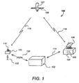
- FIG. 1 is a diagram illustrating an overview of a single satellite video distribution system
- FIG. 2 is a block diagram showing a typical uplink configuration for a single satellite transponder
- FIG. 3A is a diagram of a representative data stream
- FIG. 3B is a diagram of a representative data packet
- FIG. 4 is a block diagram showing one embodiment of the modulator for the uplink signal
- FIG. 5 is a block diagram of an integrated receiver/decoder (IRD);
- FIGS. 6A - 6C are diagrams illustrating the basic relationship of signal layers in a layered modulation transmission
- FIGS. 7A - 7C are diagrams illustrating a signal constellation of a second transmission layer over the first transmission layer after first layer demodulation
- FIG. 8A is a diagram showing a system for transmitting and receiving layered modulation signals
- FIG. 8B is a diagram showing an exemplary satellite transponder for receiving and transmitting layered modulation signals
- FIG. 9 is a block diagram depicting one embodiment of an enhanced IRD capable of receiving layered modulation signals
- FIG. 10A is a block diagram of one embodiment of the enhanced tuner/modulator and FEC encoder
- FIG. 10B depicts another embodiment of the enhanced tuner/modulator wherein layer subtraction is performed on the received layered signal
- FIG. 11A depicts the relative power levels of example embodiments of the present invention.
- FIG. 12 illustrates an exemplary computer system that could be used to implement selected modules or functions the present invention
- FIG. 13 is a diagram illustrating exemplary method steps that can be used to practice one embodiment of the invention.
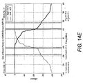
- FIGS. 14A-14E illustrate the guard band as used in a layered modulation application
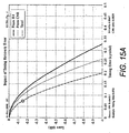
- FIGS. 15A and 15B illustrate the impact of excess bandwidth ration on symbol timing error
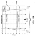
- FIGS. 16A-16H illustrate some exemplary layered modulation schemes
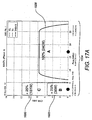
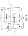
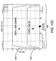
- FIGS. 17A-17C illustrate a three-phased implementation plan for upgrading an existing satellite television system.
- layered modulation reconstructs the upper layer signal and removes it from the received signal to leave a lower-layer signal.
- Lower layer signal demodulation performance requires good signal cancellation, which in turn requires the reconstructed signal to include accurate amplitude and phase effects from signal propagation path, filter and low noise block (LNB). Values of these parameters change from receiver to receiver and therefore must be estimated at each receiver.
- One difficulty with the implementation of the layered modulation techniques is that the upper layer signal requires excessive satellite TWTA power beyond the current levels for a typical continental United States (CONUS) coverage.
- the present invention reduces the required powers to levels to current conventional TWTA power limits. Therefore, there is no need to wait for TWTA power technology to further develop before layered modulation can be implemented.
- the disclosed signal schemes further increase the information throughput with layered modulation since the entire bandwidth is used more efficiently.
- the DIRECTV and GALAXY LATIN AMERICA systems combined have more than 10 million subscribers receiving QPSK signals from satellites.
- the conventional method of increasing information throughput over existing transponders would directly switching to a higher order modulation scheme such as 8PSK or 16 QAM.
- this approach would require a changeover of all IRDs in the field to be able to receive the new signal.
- deployment with the techniques of this invention (and Utility Application Serial No. 09/844,401 ) would allow existing IRDs to continue receiving the legacy signal without modification.
- New and/or upgraded subscribers would employ a new IRD to receive the new signal in addition to the legacy signal, both of which share the bandwidth.
- the potential savings of this transition is hundreds of million dollars, representing the costs of mandatory replacement of all existing IRDs.
- a changeover of all IRDs over a short time period, as required by the conventional approach would be logistically infeasible.
- the layered modulation technique can be used in communication systems outside of satellite television systems such as DIRECTV.
- VSAT very small aperture terminal
- Another example would be throughput increases for two-way voice and data communications systems using geosynchronous and low Earth orbit (LEO) satellites.
- LEO geosynchronous and low Earth orbit
- Still other possibilities include BWC and non-BWC applications of digital terrestrial broadcasting, digital cable, and cable modem services.
- layered modulation can also be used to provide higher throughputs than conventional waveforms using the same power levels.
- QPSK and/or 8PSK for modulation layers for a new-service system, there will be no need for highly linear transponder TWTAs and/or special methods to adequately compensate for TWTA nonlinearity.
- Layered modulation can therefore achieve the high spectral efficiency of the 16 QAM modulation with its two-layered QPSK modulation.
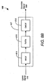
- FIG. 1 is a diagram illustrating an overview of a single satellite video distribution system 100.
- the video distribution system 100 is comprised of a control center 102 in communication with an uplink center 104 via a ground or other link 114 and with a subscriber receiver station 110 via a public switched telephone network (PSTN) or other link 120.
- the control center 102 provides program material (e.g. video programs, audio programs and data) to the uplink center 104 and coordinates with the subscriber receiver stations 110 to offer, for example, pay-per-view (PPV) program services, including billing and associated decryption of video programs.
- program material e.g. video programs, audio programs and data
- PSV pay-per-view
- the uplink center 104 receives program material and program control information from the control center 102, and using an uplink antenna 106 and transmitter 105, transmits the program material and program control information to the satellite 108 via uplink signal 116.
- the satellite receives and processes this information, and transmits the video programs and control information to the subscriber receiver station 110 via downlink signal 118 using transmitter 107.
- the subscriber receiving station 110 receives this information using the outdoor unit (ODU) 112, which includes a subscriber antenna and a low noise block converter (LNB).
- ODU outdoor unit
- LNB low noise block converter
- the subscriber receiving station antenna is an 18-inch slightly oval-shaped. Ku-band antenna.
- the slight oval shape is due to the 22.5 degree offset feed of the LNB (low noise block converter) which is used to receive signals reflected from the subscriber antenna.
- the offset feed positions the LNB out of the way so it does not block any surface area of the antenna minimizing attenuation of the incoming microwave signal.
- the video distribution system 100 can comprise a plurality of satellites 108 in order to provide wider terrestrial coverage, to provide additional channels, or to provide additional bandwidth per channel.
- each satellite is comprised of 16 transponders to receive and transmit program material and other control data from the uplink center 104 and provide it to the subscriber receiving stations 110.
- the channel capabilities two satellites 108 working together can receive and broadcast over 150 conventional (non-HDTV) audio and video channels via 32 transponders.
- the foregoing has been described with respect to an embodiment in which the program material delivered to the subscriber 122 is video (and audio) program material such as a movie, the foregoing method can be used to deliver program material comprised of purely audio information or other data as well.
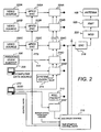
- FIG. 2 is a block diagram showing a typical uplink configuration for a single satellite 108 transponder, showing how video program material is uplinked to the satellite 108 by the control center 102 and the uplink center 104.
- FIG. 2 shows three video channels (which may be augmented respectively with one or more audio channels for high fidelity music, soundtrack information, or a secondary audio program for transmitting foreign languages), a data channel from a program guide subsystem 206 and computer data information from a computer data source 208.
- Typical video channels are provided by a program source 200A-200C of video material (collectively referred to hereinafter as program source(s) 200).
- the data from each program source 200 is provided to an encoder 202A-202C (collectively referred to hereinafter as encoder(s) 202).
- encoder(s) 202 Each of the encoders accepts a program time stamp (PTS) from the controller 216.
- PTS is a wrap-around binary time stamp that is used to assure that the video information is properly synchronized with the audio information after encoding and decoding.
- a PTS time stamp is sent with each I-frame of the MPEG encoded data.
- each encoder 202 is a second generation Motion Picture Experts Group (MPEG-2) encoder, but other decoders implementing other coding techniques can be used as well.
- the data channel can be subjected to a similar compression scheme by an encoder (not shown), but such compression is usually either unnecessary, or performed by computer programs in the computer data source (for example, photographic data is typically compressed into *.TIF files or *.JPG files before transmission).
- the signals are converted into data packets by a packetizer 204A-204F (collectively referred to hereinafter as packetizer(s) 204) associated with each program source 200.
- the output data packets are assembled using a reference from the system clock 214 (SCR), and from the conditional access manager 210, which provides the service channel identifier (SCID) to the packetizers 204 for use in generating the data packets. These data packets are then multiplexed into serial data and transmitted.
- SCR system clock 214
- SCID service channel identifier
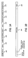
- FIG. 3A is a diagram of a representative data stream.
- the first packet 302 is comprised of information from video channel 1 (data coming from, for example, the first video program source 200A).
- the next packet 304 is comprised of computer data information that was obtained, for example from the computer data source 208.
- the next packet 306 is comprised of information from video channel 5 (from one of the video program sources 200).
- the next packet 308 is comprised of program guide information such as the information provided by the program guide subsystem 206.
- null packets 310 created by the null packet module 212 may be inserted into the data stream as desired followed by further data packets 312, 314, 316 from the program sources 200.
- the data stream therefore is comprised of a series of packets (302-316) from any one of the data sources (e.g. program sources 200, program guide subsystem 206, computer data source 208) in an order determined by the controller 216.
- the data stream is encrypted by the encryption module 218, modulated by the modulator 220 (typically using a QPSK modulation scheme), and provided to the transmitter 105, which broadcasts the modulated data stream on a frequency bandwidth to the satellite via the antenna 106.
- the receiver 500 at the receiver station 110 receives these signals, and using the SCID, reassembles the packets to regenerate the program material for each of the channels.
- FIG. 3B is a diagram of a data packet.
- Each data packet (e.g. 302-316) is 147 bytes long, and is comprised of a number of packet segments.
- the first packet segment 320 is comprised of two bytes of information containing the SCID and flags.
- the SCID is a unique 12-bit number that uniquely identifies the data packet's data channel.
- the flags include 4 bits that are used to control other features.
- the second packet segment 322 is made up of a 4-bit packet type indicator and a 4 -bit continuity counter.
- the packet type generally identifies the packet as one of the four data types (video, audio, data, or null). When combined with the SCID, the packet type determines how the data packet will be used.
- the continuity counter increments once for each packet type and SCID.
- the next packet segment 324 is comprised of 127 bytes of payload data, which in the cases of packets 302 or 306 is a portion of the video program provided by the video program source 200.
- the final packet segment 326 is data required to perform forward error correction.
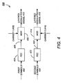
- FIG. 4 is a block diagram showing one embodiment of the modulator 220.
- the modulator 220 optionally is comprised of a forward error correction (FEC) encoder 404 which accepts the first signal symbols 402 and adds redundant information that are used to reduce transmission errors.
- the coded symbols 405 are modulated by modulator 406 according to a first carrier 408 to produce an upper layer modulated signal 410.
- Second symbols 420 are likewise provided to an optional second FEC encoder 422 to produce coded second symbols 424.
- the coded second symbols 424 are provided to a second modulator 414, which modulates the coded second signals 424 according to a second carrier 416 to produce a lower layer modulated signal 418.
- the upper layer modulated signal 410 and the lower layer modulated signal 418 are therefore uncorrelated.
- the upper layer signal 410 and the lower layer signal 418 can be transmitted to separate transponders on one or more satellites 108 via separate uplink signals 116.
- the lower layer signal 418 can be implemented from a separate satellite 108 that receives a separate uplink signal 116.
- the upper layer signal 410 must be a sufficiently greater amplitude signal than the lower layer signal 418, to maintain the signal constellations shown in FIG. 6 and FIG. 7 .
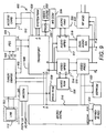
- FIG. 5 is a block diagram of an integrated receiver/decoder (IRD) 500 (also hereinafter alternatively referred to as receiver 500).
- the receiver 500 is comprised of a tuner/demodulator 504 communicatively coupled to an ODU 112 having one or more low noise blocks (LNBs) 502.
- LNBs low noise blocks
- the LNB 502 converts the 12.2- to 12.7 GHz downlink 118 signal from the satellites 108 to, e.g., a 950-1450 MHz signal required by the IRD's 500 tuner/demodulator 504.
- the LNB 502 may provide either a dual or a single output.
- the single-output LNB 502 has only one RF connector, while the dual output LNB 502 has two RF output connectors and can be used to feed a second tuner 504, a second receiver 500, or some other form of distribution system.
- the tuner/demodulator 504 isolates a single, digitally modulated 24 MHz transponder signal, and converts the modulated data to a digital data stream.
- the digital data stream is then supplied to a forward error correction (FEC) decoder 506.
- FEC forward error correction
- the error-corrected data may be fed from the FEC decoder module 506 to the transport module 508 via an 8-bit parallel interface.
- the transport module 508 performs many of the data processing functions performed by the IRD 500.
- the transport module 508 processes data received from the FEC decoder module 506 and provides the processed data to the video MPEG decoder 514 and the audio MPEG decoder 517.
- the transport module employs system RAM 528 to process the data.
- the transport module 508, video MPEG decoder 514 and audio MPEG decoder 517 are all implemented on integrated circuits. This design promotes both space and power efficiency, and increases the security of the functions performed within the transport module 508.
- the transport module 508 also provides a passage for communications between the microcontroller 510 and the video and audio MPEG decoders 514, 517. As set forth more fully hereinafter, the transport module also works with the conditional access module (CAM) 512 to determine whether the receiver 500 is permitted to access certain program material. Data from the transport module 508 can also be supplied to external communication module 526.
- CAM conditional access module
- the CAM 512 functions in association with other elements to decode an encrypted signal from the transport module 508.
- the CAM 512 may also be used for tracking and billing these services.
- the CAM 512 is a removable smart card, having contacts cooperatively interacting with contacts in the IRD 500 to pass information.
- the IRD 500, and specifically the transport module 508 provides a clock signal to the CAM 512.
- Video data is processed by the MPEG video decoder 514.
- the MPEG video decoder 514 decodes the compressed video data and sends it to an encoder or video processor 516, which converts the digital video information received from the video MPEG module 514 into an output signal usable by a display or other output device.
- processor 516 may comprise a National TV Standards Committee (NTSC) or Advanced Television Systems Committee (ATSC) encoder.
- NTSC National TV Standards Committee
- ATSC Advanced Television Systems Committee
- S-Video and ordinary video (NTSC or ATSC) signals are provided.
- Other outputs may also be utilized, and are advantageous if high definition programming is processed.
- Audio data is likewise decoded by the MPEG audio decoder 517.
- the decoded audio data may then be sent to a digital to analog (D/A) converter 518.
- the D/A converter 518 is a dual D/A converter, one for the right and left channels. If desired, additional channels can be added for use in surround sound processing or secondary audio programs (SAPs).
- SAPs secondary audio programs
- the dual D/A converter 518 itself separates the left and right channel information, as well as any additional channel information.
- Other audio formats may similarly be supported. For example, other audio formats such as multi-channel DOLBY DIGITAL AC-3 may be supported.
- the microcontroller 510 receives and processes command signals from a remote control, an IRD 500 keyboard interface, and/or other suitable input device 524.
- the microcontroller 510 receives commands for performing its operations from a processor programming memory, which permanently stores such instructions for performing such commands.
- the processor programming memory may comprise a read only memory (ROM) 538, an electrically erasable programmable read only memory (EEPROM) 522 or, similar memory device.
- the microcontroller 510 also controls the other digital devices of the IRD 500 via address and data lines (denoted "A" and "D" respectively, in FIG. 5 ).
- the modem 540 connects to the customer's phone line via the PSTN port 120. It calls, e.g. the program provider, and transmits the customer's purchase information for billing purposes, and/or other information.
- the modem 540 is controlled by the microprocessor 510.
- the modem 540 can output data to other I/O port types including standard parallel and serial computer I/O ports.
- the present invention also is comprised of a local storage unit such as the video storage device 532 for storing video and/or audio data obtained from the transport module 508.
- Video storage device 532 can be a hard disk drive, a read/writable compact disc of DVD, a solid state RAM, or any other suitable storage medium.
- the video storage device 532 is a hard disk drive with specialized parallel read/write capability so that data may be read from the video storage device 532 and written to the device 532 at the same time.
- additional buffer memory accessible by the video storage 532 or its controller may be used.
- a video storage processor 530 can be used to manage the storage and retrieval of the video data from the video storage device 532.
- the video storage processor 530 may also comprise memory for buffering data passing into and out of the video storage device 532. Alternatively or in combination with the foregoing, a plurality of video storage devices 532 can be used. Also alternatively or in combination with the foregoing, the microcontroller 510 can also perform the operations required to store and or retrieve video and other data in the video storage device 532.
- the video processing module 516 input can be directly supplied as a video output to a viewing device such as a video or computer monitor.
- the video and/or audio outputs can be supplied to an RF modulator 534 to produce an RF output and/or 8 vestigal side band (VSB) suitable as an input signal to a conventional television tuner. This allows the receiver 500 to operate with televisions without a video output.
- a viewing device such as a video or computer monitor.
- the video and/or audio outputs can be supplied to an RF modulator 534 to produce an RF output and/or 8 vestigal side band (VSB) suitable as an input signal to a conventional television tuner.
- VSB vestigal side band
- Each of the satellites 108 is comprised of a transponder, which accepts program information from the uplink center 104, and relays this information to the subscriber receiving station 110.
- Known multiplexing techniques are used so that multiple channels can be provided to the user. These multiplexing techniques include, by way of example, various statistical or other time domain multiplexing techniques and polarization multiplexing.
- a single transponder operating at a single frequency band carries a plurality of channels identified by respective service channel identification (SCID).
- SCID service channel identification
- the IRD 500 also receives and stores a program guide in a memory available to the microcontroller 510.
- the program guide is received in one or more data packets in the data stream from the satellite 108.
- the program guide can be accessed and searched by the execution of suitable operation steps implemented by the microcontroller 510 and stored in the processor ROM 538.
- the program guide may include data to map viewer channel numbers to satellite transponders and service channel identifications (SCIDs), and also provide TV program listing information to the subscriber 122 identifying program events.
- SCIDs service channel identifications
- the functionality implemented in the IRD 500 depicted in FIG. 5 can be implemented by one or more hardware modules, one or more software modules defining instructions performed by a processor, or a combination of both.
- the present invention provides for the modulation of signals at different power levels and advantageously for the signals to be non-coherent from each layer.
- independent modulation and coding of the signals may be performed.
- Backwards compatibility with legacy receivers, such as a quadrature phase shift keying (QPSK) receiver is enabled and new services are provided to new receivers.
- QPSK quadrature phase shift keying
- a typical new receiver of the present invention uses two demodulators and one remodulator as will be described in detail hereafter.
- the legacy QPSK signal is boosted in power to a higher transmission (and reception) level. This creates a power "room” in which a new lower layer signal may operate.
- the legacy receiver will not be able to distinguish the new lower layer signal, from additive white Gaussian noise, and thus operates in the usual manner.
- the optimum selection of the layer power levels is based on accommodating the legacy equipment, as well as the desired new throughput and services.
- the new lower layer signal is provided with a sufficient carrier to thermal noise ratio to function properly.
- the new lower layer signal and the boosted legacy signal are non-coherent with respect to each other. Therefore, the new lower layer signal can be implemented from a different TWTA and even from a different satellite.
- the new lower layer signal format is also independent of the legacy format, e.g., it may be QPSK or 8PSK, using the conventional concatenated FEC code or using a new Turbo code.
- the lower layer signal may even be an analog signal.
- the combined layered signal is demodulated and decoded by first demodulating the upper layer to remove the upper carrier.
- the stabilized layered signal may then have the upper layer FEC decoded and the output upper layer symbols communicated to the upper layer transport.
- the upper layer symbols are also employed in a remodulator, to generate an idealized upper layer signal.
- the idealized upper layer signal is then subtracted from the stable layered signal to reveal the lower layer signal.
- the lower layer signal is then demodulated and FEC decoded and communicated to the lower layer transport.
- Signals, systems and methods using the present invention may be used to supplement a pre-existing transmission compatible with legacy receiving hardware in a backwards-compatible application or as part of a preplanned layered modulation architecture providing one or more additional layers at a present or at a later date.
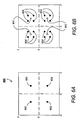
- FIGS. 6A - 6C illustrate the basic relationship of signal layers in a received layered modulation transmission.
- FIG. 6A illustrates an upper layer signal constellation 600 of a transmission signal showing the signal points or symbols 602.
- FIG. 6B illustrates the lower layer signal constellation of symbols 604 over the upper layer signal constellation 600 where the layers are coherent (or synchronized).
- FIG. 6C illustrates a lower layer signal 606 of a second transmission layer over the upper layer constellation where the layers are non-coherent.
- the lower layer 606 rotates about the upper layer constellation 602 due to the relative modulating frequencies of the two layers in a non-coherent transmission. Both the upper and lower layers rotate about the origin due to the first layer modulation frequency as described by path 608.
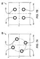
- FIGS. 7A - 7C are diagrams illustrating a non-coherent relationship between a lower transmission layer over the upper transmission layer after upper layer demodulation.
- FIG. 7A shows the constellation 700 before the first carrier recovery loop (CRL) of the upper layer and The constellation rings 702 rotate around the large radius circle indicated by the dashed line.
- FIG. 7B shows the constellation 704 after CRL of the upper layer where the rotation of the constellation rings 702 is stopped.
- the constellation rings 702 are the signal points of the lower layer around the nodes 602 of the upper layer.
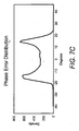
- FIG. 7C depicts a phase distribution of the received signal with respect to nodes 602.
- Relative modulating frequencies of the non-coherent upper and lower layer signals cause the lower layer constellation to rotate around the nodes 602 of the upper layer constellation to form rings 702. After the lower layer CRL this rotation is eliminated and the nodes of the lower layer are revealed (as shown in FIG. 6B ).
- the radius of the lower layer constellation rings 702 is indicative of the lower layer power level.
- the thickness of the rings 702 is indicative of the carrier to noise ratio (CNR) of the lower layer.
- CNR carrier to noise ratio
- the lower layer may be used to transmit distinct digital or analog signals.
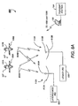
- FIG. 8A is a diagram showing a system for transmitting and receiving layered modulation signals.
- Separate transmitters 107A, 107B (which include TWTAs to amplify the signals), as may be located on any suitable platform, such a satellites 108A, 108B, are used to non-coherently transmit different layers of a signal of the present invention.
- Each satellite includes additional transmitters 107C, 107D which can be used to transmit additional signals (from additional received uplink signals) to be used in the frequency bandwidth of the layered signal as detailed hereafter.
- Uplink signals 116 are typically transmitted to each satellite 108A, 108B from one or more uplink centers 104 with one or more transmitters 105 via an antenna 106.
- FIG. 8B is a diagram illustrating an exemplary satellite transponder 107 for receiving and transmitting layered modulation signals on a satellite 108.
- the uplink signal 116 is received by the satellite 108 and passed through a input multiplexer (IMUX) 814. Following this the signal is amplified with a travelling wave tube amplifier (TWTA) 816 and then through an output muliplexer (OMUX) 818 before the downlink signal 118 is transmitted to the receivers 802, 500.
- IMUX input multiplexer
- TWTA travelling wave tube amplifier
- OFMUX output muliplexer
- the layered signals 808A, 808B (e.g. multiple downlink signals 118) are received at receiver antennas 812A, 812B, such as satellite dishes, each with a low noise block (LNB) 810A, 810B where they are then coupled to integrated receiver/decoders (IRDs) 500, 802.
- LNB low noise block
- IRDs integrated receiver/decoders
- first satellite 108A and transmitter 107A can transmit an upper layer legacy signal 808A
- second satellite 108B and transmitter 107B can transmit a lower layer signal 808B.
- both signals 808A, 808B arrive at each antenna 812A, 812B and LNB 810A, 810B, only the layer modulation IRD 802 is capable of decoding both signals 808A, 808B.
- the legacy receiver 500 is only capable of decoding the upper layer legacy signal 808A; the lower layer signal 808B appears only as noise to the legacy receiver 500.
- any composite signal, including new additional signal layers will be backwards compatible with legacy receivers 500, which will disregard the new signal layers.
- the combined signal and noise level for the lower layer must be at or below the allowed noise floor for the upper layer at the particular receiver antenna 812A, 812B.
- Layered modulation applications include backwards compatible and non-backwards compatible applications.
- “Backwards compatible” in this sense, describes systems in which legacy receivers 500 are not rendered obsolete by the additional signal layer(s). Instead, even if the legacy receivers 500 are incapable of decoding the additional signal layer(s), they are capable of receiving the layered modulated signal and decoding the original signal layer. In these applications, the pre-existing system architecture is accommodated by the architecture of the additional signal layers.
- Non-backwards compatible describes a system architecture which makes use of layered modulation, but the modulation scheme employed is such that pre-existing equipment is incapable of receiving and decoding the information on additional signal layer(s).
- the pre-existing legacy IRDs 500 decode and make use of data only from the layer (or layers) they were designed to receive, unaffected by the additional layers.
- the legacy signals may be modified to optimally implement the new layers.
- the present invention may be applied to existing direct satellite services which are broadcast to individual users in order to enable additional features and services with new receivers without adversely affecting legacy receivers and without requiring additional signal frequency.
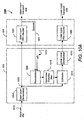
- FIG. 9 is a block diagram depicting one embodiment of an enhanced IRD 802 capable of receiving layered modulation signals.
- the IRD includes many similar components as that of the legacy IRD 500 of FIG. 5 .
- the enhanced IRD 802 includes a feedback path 902 in which the FEC decoded symbols are fed back to a enhanced modified tuner/demodulator 904 and transport module 908 for decoding both signal layers as detailed hereafter.
- FIG. 10A is a block diagram of one embodiment of the enhanced tuner/modulator 904 and FEC encoder 506.
- FIG. 10A depicts reception where layer subtraction is performed on a signal where the upper layer carrier has already been demodulated.
- the upper layer of the received combined signal 1016 from the LNB 502, which may contain legacy modulation format, is provided to and processed by an upper layer demodulator 1004 to produce the stable demodulated signal 1020.
- the demodulated signal 420 is communicatively coupled to a FEC decoder 402 which decodes the upper layer to produce the upper layer symbols which are output to an upper layer transport module 908.
- the upper layer symbols are also used to generate an idealized upper layer signal.
- the upper layer symbols may be produced from the decoder 402 after Viterbi decode (BER ⁇ 10 -3 or so) or after Reed-Solomon (RS) decode (BER ⁇ 10 -9 or so), in typical decoding operations known to those skilled in the art.
- the upper layer symbols are provided via feedback path 902 from the upper layer decoder 402 to a remodulator 406 which effectively produces an idealized upper layer signal.
- the idealized upper level signal is subtracted from the demodulated upper layer signal 1020.
- the modulated signal may have been distorted, for example, by traveling wave tube amplifier (TWTA) non-linearity or other non-linear or linear distortions in the transmission channel.
- TWTA traveling wave tube amplifier
- the distortion effects are estimated from the received signal after the fact or from TWTA characteristics which may be downloaded into the IRD in AM - AM and/or AM - PM maps 1014, used to eliminate the distortion.
- a subtractor 1012 then subtracts the idealized upper layer signal from the stable demodulated signal 1020. This leaves the lower-power second layer signal.
- the subtractor 1012 may include a buffer or delay function to retain the stable demodulated signal 1020 while the idealized upper layer signal is being constructed.
- the second layer signal is demodulated by the lower level demodulator 1010 and FEC decoded by decoder 1008 according to its signal format to produce the lower layer symbols, which are provided to the transport module 908.
- FIG. 10B depicts another embodiment wherein layer subtraction is performed on the received layered signal (prior to upper layer demodulation).
- the upper layer demodulator 1004 produces the upper carrier signal 1022 (as well as the stable demodulated signal output 1020).
- An upper carrier signal 1022 is provided to the remodulator 1006.
- the remodulator 1006 provides the remodulated signal to the non-linear distortion mapper 1018 which effectively produces an idealized upper layer signal.
- the idealized upper layer signal includes the upper layer carrier for subtraction from the received combined signal 808A, 808B.
- M U is the magnitude of the upper layer QPSK signal
- M L is the magnitude of the lower layer QPSK signal
- M L ⁇ M U .
- the signal frequencies and phase for the upper and lower layer signals are respectively ⁇ U , ⁇ U and ⁇ U , ⁇ U .
- the symbol timing misalignment between the upper and lower layers is ⁇ T m .
- p ( t - mT ) represents the time shifted version of the pulse shaping filter p ( t ) 414 employed in signal modulation.
- f U ( ⁇ ) and f L ( ⁇ ) denote the distortion function of the TWTAs for the respective signals.
- the upper and lower layer frequencies are substantially equal. Significant improvements in system efficiency can be obtained by using a frequency offset between layers.
- two-layered backward compatible modulation with QPSK doubles a current 6/7 rate capacity by adding a TWTA approximately 6.2 dB above an existing TWTA power.
- New QPSK signals may be transmitted from a separate transmitter, from a different satellite for example.
- TWTAs linear travelling wave tube amplifiers
- 16QAM phase error penalty
- the relationship between the individual modulation layers can be structured to facilitate backward compatible applications.
- a new layer structure can be designed to optimize the combined efficiency and/or performance of the layered modulation system.
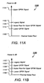
- FIG. 11A depicts the relative power levels 1100 of example embodiments of the present invention.
- FIG. 11A is not a scale drawing.
- This embodiment doubles the pre-existing rate 6/7 capacity by using a TWTA 6.2 dB above a pre-existing TWTA equivalent isotropic radiated power (EIRP) and second TWTA 2 dB below the pre-existing TWTA power.
- EIRP isotropic radiated power
- This embodiment uses upper and lower QPSK layers which are non-coherent.
- a code rate of 6/7 is also used for both layers.
- the signal of the legacy QPSK signal 1102 is used to generate the upper layer 1104 and a new QPSK layer is the lower layer 1110.
- the CNR of the legacy QPSK signal 1102 is approximately 7 dB.
- the legacy QPSK signal 1102 is boosted in power by approximately 6.2 dB bringing the new power level to approximately 13.2 dB as the upper layer 1104.
- the noise floor 1106 of the upper layer is approximately 6.2 dB.
- the new lower QPSK layer 1110 has a CNR of approximately 5 dB.
- the total signal and noise of the lower layer is kept at or below the tolerable noise floor 1106 of the upper layer.
- the power boosted upper layer 1104 of the present invention is also very robust, making it resistant to rain fade. It should be noted that the invention may be extended to multiple layers with mixed modulations, coding and code rates.
- a code rate of 2/3 may be used for both the upper and lower layers 1104, 1110.
- the CNR of the legacy QPSK signal 1102 (with a code rate of 2/3) is approximately 5.8 dB.
- the legacy signal 1102 is boosted by approximately 5.3 dB to approximately 11.1 dB (4.1 dB above the legacy QPSK signal 1102 with a code rate of 2/3) to form the upper QPSK layer 1104.
- the new lower QPSK layer 1110 has a CNR of approximately 3.8 dB.
- the total signal and noise of the lower layer 1110 is kept at or below approximately 5.3 dB, the tolerable noise floor 1106 of the upper QPSK layer. In this case, overall capacity is improved by 1.55 and the effective rate for legacy IRDs will be 7/9 of that before implementing the layered modulation.
- the code rates between the upper and lower layers 1104, 1110 may be mixed.
- the legacy QPSK signal 502 may be boosted by approximately 5.3 dB to approximately 12.3 dB with the code rate unchanged at 6/7 to create the upper QPSK layer 1104.
- the new lower QPSK layer 1110 may use a code rate of 2/3 with a CNR of approximately 3.8 dB.
- the total capacity relative to the legacy signal 1102 is approximately 1.78.
- the legacy IRDs will suffer no significant rate decrease.
- the present invention may also be used in "non-backward compatible" applications.
- two QPSK layers 1104, 1110 are used each at a code rate of 2/3.
- the upper QPSK layer 504 has a CNR of approximately 4.1 dB above its noise floor 1106 and the lower QPSK layer 1110 also has a CNR of approximately 4.1 dB.
- the total code and noise level of the lower QPSK layer 1110 is approximately 5.5 dB.
- the total CNR for the upper QPSK signal 1104 is approximately 9.4 dB, merely 2.4 dB above the legacy QPSK signal rate 6/7.
- the capacity is approximately 1.74 compared to the legacy rate 6/7.
- FIG. 11B depicts the relative power levels of an alternate embodiment wherein both the upper and lower layers 1104, 1110 are below the legacy signal level 1102.
- the two QPSK layers 1104, 1110 use a code rate of 1/2.
- the upper QPSK layer 1104 is approximately 2.0 dB above its noise floor 1106 of approximately 4.1 dB.
- the lower QPSK layer has a CNR of approximately 2.0 dB and a total code and noise level at or below 4.1 dB.
- the capacity of this embodiment is approximately 1.31 compared to the legacy rate 6/7.
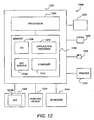
- FIG. 12 illustrates an exemplary computer system 1200 that could be used to implement selected modules and/or functions of the present invention.
- the computer 1202 is comprised of a processor 1204 and a memory 1206, such as random access memory (RAM).
- the computer 1202 is operatively coupled to a display 1222, which presents images such as windows to the user on a graphical user interface 1218B.
- the computer 1202 may be coupled to other devices, such as a keyboard 1214, a mouse device 1216, a printer, etc.
- a keyboard 1214 such as a keyboard 1214, a mouse device 1216, a printer, etc.
- the computer 1202 operates under control of an operating system 1208 stored in the memory 1206, and interfaces with the user to accept inputs and commands and to present results through a graphical user interface (GUI) module 1218A.
- GUI graphical user interface
- the instructions performing the GUI functions can be resident or distributed in the operating system 1208, the computer program 1210, or implemented with special purpose memory and processors.
- the computer 1202 also implements a compiler 1212 which allows an application program 1210 written in a programming language such as COBOL, C++, FORTRAN, or other language to be translated into processor 1204 readable code.
- the application 1210 accesses and manipulates data stored in the memory 1206 of the computer 1202 using the relationships and logic that was generated using the compiler 1212.
- the computer 1202 also optionally is comprised of an external communication device such as a modem, satellite link, Ethernet card, or other device for communicating with other computers.
- instructions implementing the operating system 1208, the computer program 1210, and the compiler 1212 are tangibly embodied in a computer-readable medium, e.g., data storage device 1220, which could include one or more fixed or removable data storage devices, such as a zip drive, floppy disc drive 1224, hard drive, CD-ROM drive, tape drive, etc.
- the operating system 1208 and the computer program 1210 are comprised of instructions which, when read and executed by the computer 1202, causes the computer 1202 to perform the steps necessary to implement and/or use the present invention.
- Computer program 1210 and/or operating instructions may also be tangibly embodied in memory 1206 and/or data communications devices 1230, thereby making a computer program product or article of manufacture according to the invention.
- the terms "article of manufacture,” “program storage device” and “computer program product” as used herein are intended to encompass a computer program accessible from any computer readable device or media.
- the layered modulation (LM) technique described above typically requires the use of transmitters of transponders in satellites 108A, 108B, with the upper layer transponder having greater power output than those associated with ordinary modulation techniques.
- the upper signal layer 808A must be modulated by a carrier of substantially higher power than the lower signal layer 808B.
- backwards compatible (BWC) applications typically require more power than non-BWC applications for the upper signal layer 808A.
- Embodiments of the present invention utilize one or more of four defined signal schemes to improve the power and spectral efficiency of system. Such improvements allow for layered modulation systems to operate at conventional TWTA power levels.
- the four signal schemes are described in detail below.
- the signal schemes can be employed separately or in combination to achieve improved performance.
- the symbol rate of the lower layer signal is reduced below the symbol rate of the upper layer signal (or vice versa if non-backwards compatible).
- the guard band providing against adjacent channel interference is reduced or eliminated.
- the excess signal bandwidth ratio, ⁇ is reduced.
- multiple signal layers can be used to provide a new data stream in the guard band of the legacy signal.
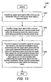
- FIG. 13 is a diagram illustrating an exemplary method 1300 that can be used to practice one embodiment of the invention.
- an upper layer signal is amplified with a first excess bandwidth ratio at a first power level within a frequency band.
- a lower layer signal is amplified with a second excess bandwidth ratio at a second power level within the frequency band, the second power level being exceeded by the first power level.
- a layered modulation signal is transmitted for at least one receiver, the layered modulation signal comprising both the upper layer signal and the lower layer signal interfering with each other within the frequency band such that the upper layer signal can be demodulated directly from the layered modulation signal and the lower layer signal can be demodulated after subtracting the upper layer signal from the layered modulation signal, wherein substantially no guard band is used within the frequency band.
- the foregoing method can be applied to implement the signal schemes described hereafter in the system architecture detailed above.
- the upper layer signal comprises a legacy signal in a satellite television system that has a reduced excess bandwidth ratio over the original legacy signal.
- the original legacy signal may have an excess bandwidth ratio of 0.2.
- the new layered signals will each have an independent bandwidth ratio that does not exceed 0.2.
- the excess bandwidth ratio for any of the layered signals can be further reduced not to exceed 0.1.
- the upper and lower layer signals can be amplified and transmitted from a common satellite and/or antenna or from different satellites and/or antennas.
- the first modulation scheme involves reducing the symbol rate of the lower layer signal, e.g., the new lower layer signal 808B operating over the upper layer legacy signal 808A.
- the symbol rate in a digital signal relates to the signal power concentrated over smaller bandwidth; doubling the symbol rate doubles the throughput and carrier power (requiring that adequate available bandwidth).
- the lower layer signal 808B occupies a narrower bandwidth. This means that a smaller amount of interference will be exhibited at the legacy signal.
- the legacy signal 808A can be operated at a lower power level than would otherwise be required to be received by a legacy receiver 500.
- a reduced symbol rate will also reduce the throughput for the lower layer signal 808B.
- a second modulation scheme requires reducing or eliminating the guard band.
- a guard band of 5.16 MHz exists between adjacent transponders of the same polarization. This is a legacy configuration from earlier satellite communication standards for analog FM transmission.
- the FM communication standard requires a relatively high CNR (on the order of 14 dB), and is therefore more susceptible to spectral re-growth effects from satellite TWTA non-linearity and other imperfections.
- the designed guard band has provided more than enough margin for the FM signal to reject spread signal energy due to adjacent channel interference (ACI).
- ACI adjacent channel interference
- the current digital Direct Broadcast Systems (DBS) signal requires a CNR on the order of 7.6 dB with prevailing QPSK modulation and concatenated forward error correction (FEC) codes.
- FEC forward error correction
- turbo-like codes such as turbo product codes, serial/parallel concatenated convolutional codes and low-density parity check codes, which provide higher coding gains than the conventional codes, the required CNR drops even lower (to around 5.4 dB for the same modulation and a similar code rate).
- turbo-like codes are referred to as advanced FEC codes in contrast with conventional codes. Again, other factors being equal, signals with smaller CNRs are less susceptible to noise and interference effects.
- a computer simulation on out-of-band (OOB) signal power ratios of a typical TWTA nonlinearity yields an OOB ratio of approximately -20 dB at ⁇ 12 MHz with an ⁇ of 0.2, and an OOB ratio of approximately -20 dB at ⁇ 11 MHz with an ⁇ of 0.1. Both these simulations assume linearized TWTAs and are conservative, based upon a "brick wall" filter for the undesired signal.
- OOB out-of-band
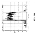
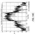
- FIGS. 14A-14E illustrate spectral outgrowth effects into the guard band.
- FIG. 14A is an exemplary computer simulated signal spectrum without TWTA nonlinearity and with an ⁇ of 0.2.
- FIG. 14B illustrates the amplitude and phase characteristics of an exemplary "linearized" satellite TWTA.
- FIG. 14C illustrates exemplary signal spectrum after processing through an output multiplexer (OMUX) on a satellite with ⁇ of 0.1. Thus, the signal has been processed through an input multiplexer (IMUX), the linearized TWTA and the OMUX,.
- FIG. 14D illustrates the out-of-band signal power ratio versus the cutoff frequency with an ⁇ of 0.2. Spectral re-growth is mostly due to TWTA non-linearity.
- FIG. 14E illustrates the out-of-band signal power ratio versus the cutoff frequency with an ⁇ of 0.1.
- f max is ⁇ 18.2 MHz and the OOB ratio is approximately -24 dB.
- the existing guard band for DIRECTV may be reduced or even eliminated with only a small impact on communication performance.
- eliminating the DIRECTV guard band could increase spectral efficiency by a factor of approximately 22% (from the ratio of 29.16/24).
- the throughput increase is achieved by increasing the symbol rate with this ratio without the need to increase the code rate which would require more power.
- ISI inter-symbol interference
- ASC advanced television systems committee
- an excess bandwidth ratio of 0.1 reduces the signal CNR by approximately 0.151 dB.
- an excess bandwidth ratio of 0.2 reduces the signal CNR by approximately 0.148 dB
- an excess bandwidth ratio of 0.35 reduces the signal CNR by approximately 0.136 dB.
- TWTA non-linearity flattens the signal waveform and therefore increases tracked timing errors. This can be compensated by imposing slightly higher linearity requirements on new TWTAs. The smaller lower layer signal power required allows the TWTA to operate closer to its linear region.
- FIGS. 15A and 15B illustrate the impact of excess bandwidth ratio on symbol timing error by computer simulations.
- FIG. 15A illustrates the symbol timing error with an excess bandwidth ratio of 0.1 for a root raised cosine filter.
- the ISI is calculated by sampling from adjacent symbols off zero-crossing points.
- the CNR reduction is calculated by sampling the signal off-peak.
- FIG. 15B illustrates the symbol timing error with an excess bandwidth ratio of 0.2. The results are very similar to that of FIG. 15A .
- One solution to mitigate this effect is to increase the power levels of the layered signals to overcome the degradation from legacy signal.
- the impact on the legacy signal from the new lower layer signal is less severe (e.g. receiver desensitization of approximately 0.2 dB).
- Both new signal layers can include an advanced FEC code.
- implementation of this modulation scheme will provide the infrastructure that can later be used to convert the system to a non-backwards compatible modulation scheme with maximized spectral efficiency.
- spectral efficiency of the legacy system can be increased by as much as 50% while remaining backwards compatible with the legacy system.
- modulation schemes are selectively applied to non-BWC applications, better power and spectral efficiencies also follow.
- use of layered modulation can increase spectral efficiency by as much as 184% with only approximately 4.3 dB of increase relative to legacy signal power.
- the 8-PSK system (with an advanced FEC code) would only achieve approximately 72% increase in spectral efficiency, while requiring a 1.2 dB power increase.
- FIGS. 16A-16H illustrate some exemplary layered modulation implementations.
- FIG. 16A illustrates a basic layered modulation implementation using a single carrier frequency for both layers with an excess bandwidth ratio of 0.2 for both the upper and lower layer signals.
- the code rate is 6/7 for both signals and spectral efficiency is 200% relative to the a legacy signal.
- Both the upper layer signal 1600 and the lower layer signal 1602 occupy the same frequency band 1604.
- a guard band 1606A, 1606B is indicated by the absence of signal on both sides of the frequency band 1604.
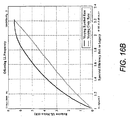
- FIG. 16B illustrates spectral efficiency of modulation schemes of the present invention compared with the basic layered modulation implementation.
- the horizontal axis is spectral efficiency relative to that of the legacy signal, and the vertical axis is the effective noise floor as seen by the upper layer signal (the lower the noise floor, the less power the upper layer signal requires). In this case, the carrier lock requirement is ignored.
- Both the upper and lower layer signals have an excess bandwidth ratio of 0.2.
- Spectral efficiency improves to a maximum of 222% of the legacy throughput as the lower layer signal includes the guard band when compared with the basic layered modulation implementation.
- the plot shows a curve for varying the symbol rate as well as varying the code rate. Varying the code rate is shown to be more power efficient than varying the symbol rate for the upper layer signal.
- FIG. 16C illustrates spectral efficiency of modulation schemes of the present invention compared with the basic layered modulation implementation, but with the carrier lock requirement considered.
- both the upper and lower layer signals have an excess bandwidth ratio of 0.2.
- spectral efficiency improves to a maximum of 222% as the lower layer signal includes the guard band when compared with the basic layered modulation implementation.
- the upper layer carrier signal operates at approximately 1080 W with a symbol rate of 20 MHz.
- the lower layer carrier signal operates at approximately 176 W with a symbol rate of 24.3 MHz.
- the plot shows a curve for varying the symbol rate as well as varying the code rate. Varying the code rate is more power efficient than varying the symbol rate down to approximately 50%, when the carrier becomes a problem.
- the maximum upper layer power increase is approximately 6.5 dB.
- a layered modulation implementation can begin with both the code rate and symbol rate maximized.
- a CNR of at least 6.5 dB should be used for the upper layer signal.
- spectral efficiency can be reduced to a desired or affordable level in terms of power requirements.
- the symbol rate is reduced, the total noise introduced by the lower layer decreases linearly.
- the lower layer signal frequency should be positioned to minimize spectral overlap with the upper layer signal frequency.
- the code rate is reduced, the total noise introduced by the lower layer signal decreases at a greater than linear rate.
- reducing the code rate is limited by the required CNR floor for the carrier lock of the lower layer signal, e.g., approximately 1.2 dB for QPSK without pilots.
- Crossover in spectral efficiency generally exists between the methods of reducing the code rate and reducing the symbol rate. Accordingly, the code rate can be selected above crossover spectral efficiency and the symbol rate selected below crossover spectral efficiency.
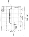
- FIG. 16D illustrates an exemplary layered modulation signal scheme where the lower layer signal is disposed in the guard band of the upper layer signal.
- the lower layer signal begins at the edge of the frequency band to minimize interference into the upper layer signal.
- the lower layer signal (guard band signal) has an excess bandwidth ratio of 0.2 and a power level of approximately 72 W.
- the upper layer signal has an excess bandwidth ratio of 0.2 and a power level of 398 W.
- the code rate is 6/7 for the legacy upper layer signal and the new-service lower layer signal. This example yields a spectral efficiency of approximately 150% compared with a legacy signal. As is shown, substantially no guard band is used within the frequency band 1604.
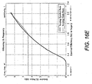
- FIG. 16E illustrates spectral efficiency of the exemplary layered modulation signal scheme of FIG 16D .
- No interference is shown with the lower layer signal bandwidth up to 5.2 MHz.
- the code rate is fixed at 6/7 for the lower layer signal.
- Spectral efficiency improves to about 150% over a legacy signal with a +2.2 dB over the legacy signal power.
- spectral efficiency of 222% is obtained with a +6.5 dB power level over the legacy signal power.
- Spectral re-growth is ignored here. Note that varying the symbol rate is more power efficient than varying the code rate up to a 180% spectral efficiency factor.
- the maximum power increase of the upper layer signal is approximately 6.5 dB.
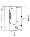
- FIG. 16F illustrates another exemplary layered modulation signal scheme where the lower layer signal is disposed in the guard band of the upper layer signal.
- the lower layer signal has an excess bandwidth ratio of 0.1 and a power level of approximately 72 W.
- the lower layer signal begins at the edge of the frequency band to minimize interference into the upper layer signal.
- the upper layer signal (legacy signal) has an excess bandwidth ratio of 0.2 and a power level of 380 W.
- the code rate is 6/7. Again, as shown, substantially no guard band is used within the frequency band 1604.
- FIG. 16G illustrates spectral efficiency of the exemplary layered modulation signal scheme of FIG 16F .
- Less interference into the upper layer signal by the lower layer signal is shown, as compared with FIG. 16E .
- spectral efficiency improves about 150% with a +2.0 dB over the legacy signal power.
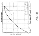
- Spectral efficiency of 232% is obtained with a +6.5 dB power level over the legacy signal power.
- the increase in spectral efficiency is because a higher symbol rate is available than with the previous example (although the lower layer signal requires approximately +0.4 dB).
- Spectral re-growth is again ignored here. Note that varying the symbol rate is more power efficient than varying the code rate for up to a 185% spectral efficiency.
- the maximum power increase of the upper layer signal is approximately 6.5 dB.
- FIG. 16H illustrates spectral efficiency of the exemplary layered modulation signal scheme where a two-layered signal is applied in the guard band. Here a steep curve is exhibited with varying symbol rate. The signal scheme is most efficient at lower symbol rates and there is little spectral overlap with the legacy signal. Spectral efficiency is about 150% with no power increase required over the legacy signal power. Spectral efficiency of 172% is obtained with only a +2 dB power level over the legacy signal power.
- FIGS. 17A-17C illustrate an exemplary three-phased implementation plan for upgrading an existing satellite television broadcast system.
- FIG. 17A illustrates a first phase where a two-layered signal is added to the guard band. Three transponders are required, one for the legacy signal and two new transponders for each layer of the guard band signal.
- the layered guard band signals each may have an excess bandwidth ratio of 0.1, while the legacy signal retains an excess bandwidth ratio of 0.2.
- the CNR for the upper and lower layer signals of the guard band are 11.9 dB and 5.4 dB respectively.
- the legacy signal employs a CNR of 7.6 dB. Accordingly, the transponder for the legacy signal need not be upgraded to implement the first phase although the layered signals may be operated from an interim satellite.
- the upper layer signal 1600 and the lower layer signal 1602 share the frequency band 1604 with a third signal 1608, the legacy signal, which occupies a majority of the frequency band.
- the upper layer signal 1600 and the lower layer signal 1602 are distinct from the third signal, i.e., the layered signals do not interfere with the third signal 1608.
- the upper layer signal and the lower layer signal are employed within the guard band of the old legacy signal.
- substantially all guard band is used within the frequency band 1604.
- FIG. 17B illustrates a second phase where two upper layer signals are spanned by one lower layer signal.
- One of the upper layer signals is the legacy signal which must have a raised power level to overcome the "noise" of the lower layer signal. Accordingly, the transponder for the legacy signal will need to be upgraded, e.g., migrated to a new satellite.
- the lower layer signal may also be migrated to another transponder, e.g., on the same new satellite.
- the CNR for the upper and lower layer signals of the guard band are 11.9 dB and 5.4 dB respectively, while the legacy signal employs a CNR of 13.1 dB. At this phase spectral efficiency increases to 230%.
- the upper layer signal 1600 and the lower layer signal 1602 share the frequency band 1604 with a third signal 1608, the legacy signal, which dominates the frequency band.
- the lower layer signal 1602 interferes with the legacy signal as well as the upper layer signal 1600. Again, substantially all guard band is used within the frequency band 1604.
- FIG. 17C illustrates a third phase where layered modulation of the whole spectrum is implemented with new signals.
- the upper layer signal substantially takes the place of the legacy signal while the lower layer signal substantially takes the place of the signal previously layered with the upper layer guard band signal.
- the CNR for the new upper and lower layer signals are 11.9 dB and 5.4 dB respectively.
- the excess bandwidth ratio is 0.1 for both signals.
- spectral efficiency increases to 264%.
- the third signal of the second phase becomes the upper layer signal 1600 over the lower layer signal 1602. Substantially all guard band is used within the frequency band 1604.
Landscapes
- Engineering & Computer Science (AREA)
- Signal Processing (AREA)
- Physics & Mathematics (AREA)
- Astronomy & Astrophysics (AREA)
- General Physics & Mathematics (AREA)
- Computer Networks & Wireless Communication (AREA)
- Aviation & Aerospace Engineering (AREA)
- Multimedia (AREA)
- Two-Way Televisions, Distribution Of Moving Picture Or The Like (AREA)
- Transmitters (AREA)
- Radio Relay Systems (AREA)
- Near-Field Transmission Systems (AREA)
Claims (12)
- Verfahren zum Senden von Signalen und Empfangen von Signalen in einem veralteten Empfänger (500) und einem Empfänger (802) mit geschichteter Modulation, gekennzeichnet durch die folgenden Schritte:Verstärken eines Teils eines Signals (410) der oberen Schicht eines Abwärtsstreckensignals mit einem ersten Bandbreitenüberschussverhältnis mit einem ersten Leistungspegel in einem Frequenzband des Abwärtsstreckensignals, wobei das Signal der oberen Schicht gemäß einem ersten Träger moduliert wird;Verstärken eines Teils eines Signals (418) der unteren Schicht des Abwärtsstreckensignals mit einem zweiten Bandbreitenüberschussverhältnis mit einem zweiten Leistungspegel in dem Frequenzband des Abwärtsstreckensignals, wobei der zweite Leistungspegel durch den ersten Leistungspegel überschritten wird, wobei das Signal der unteren Schicht gemäß einem zweiten Träger moduliert wird;Senden eines Signals (1016) geschichteter Modulation, wobei das Signal (1016) geschichteter Modulation sowohl den verstärkten Signalteil (410) der oberen Schicht als auch den verstärkten Signalteil (418) der unteren Schicht umfasst, die sich in dem Frequenzband stören, wobei der verstärkte Signalteil (410) der oberen Schicht durch einen ersten Transponder und der verstärkte Signalteil der unteren Schicht durch einen zweiten Transponder gesendet wird, der mit derselben Polarisation sendet;Demodulieren des Signals (410) der oberen Schicht direkt aus dem Signal geschichteter Modulation gemäß dem ersten Träger in einem veralteten Empfänger und in einem Empfänger (802) geschichteter Modulation; undDemodulieren des Signals (418) der unteren Schicht gemäß dem zweiten Träger nach Subtrahieren eines neumodulierten Signals (410) der oberen Schicht von dem Signal (1016) geschichteter Modulation in dem Empfänger geschichteter Modulation und nicht in dem veralteten Empfänger;wobei das Signal der oberen Schicht und das Signal der unteren Schicht nichtkohärent sind.
- Verfahren nach Anspruch 1, wobei der Signalteil (418) der unteren Schicht eine Symbolrate der unteren Schicht umfasst, der Signalteil (410) der oberen Schicht eine Symbolrate der oberen Schicht umfasst und wobei die Symbolrate der unteren Schicht kleiner als die Symbolrate der oberen Schicht ist.
- Verfahren nach Anspruch 1 oder Anspruch 2, wobei im Wesentlichen kein Schutzband in dem Frequenzband verwendet wird.
- Verfahren nach einem der Ansprüche 1, 2 und 3, wobei das erste Bandbreitenüberschussverhältnis und/oder das zweite Bandbreitenüberschussverhältnis 0,1 nicht überschreitet.
- Verfahren nach Anspruch 3, wobei der Signalteil der oberen Schicht mit einem ersten Modulationsschema moduliert wird und der Signalteil der unteren Schicht mit einem zweiten Modulationsschema moduliert wird, das von dem ersten Modulationsschema verschieden ist.
- Verfahren nach einem der Ansprüche 1, 2 und 3, das ferner den folgenden Schritt umfasst:Verstärken eines dritten Signalteils des Abwärtsstreckensignals, wobei der dritte Signalteil ein drittes Bandbreitenüberschussverhältnis aufweist und durch die mindestens eine Antenne gesendet wird, um einen größten Teil des Frequenzbands des Abwärtsstreckensignals einzunehmen;wobei das Signal der oberen Schicht und das Signal der unteren Schicht in einem Rest des Frequenzbandes des Abwärtsstreckensignals gesendet werden und der dritte Signalteil ein veraltetes Signal umfasst und das dritte Bandbreitenüberschussverhältnis 0,2 nicht überschreitet und das erste Bandbreitenüberschussverhältnis und das zweite Bandbreitenverhältnis 0,1 nicht überschreiten.
- Verfahren nach einem der Ansprüche 1, 2 und 3, wobei das Signal der oberen Schicht ein veraltetes Signal in einem Satellitenfernsehsystem umfasst.
- Satellitenfernsehsystem zum Senden von Signalen und Empfangen von Signalen, gekennzeichnet durch
einen ersten Verstärker (816) zum Verstärken eines Teils eines Signals (410) der oberen Schicht eines Abwärtsstreckensignals mit einem ersten Bandbreitenüberschussverhältnis mit einem ersten Leistungspegel in einem Frequenzband des Abwärtsstreckensignals, wobei das Signal der oberen Schicht gemäß einem ersten Träger moduliert wird und ein veraltetes Signal in dem Satellitenfernsehsystem umfasst;
einen zweiten Verstärker (816) zum Verstärken eines Teils eines Signals (418) der unteren Schicht des Abwärtsstreckensignals mit einem zweiten Bandbreitenüberschussverhältnis mit einem zweiten Leistungspegel in dem Frequenzband des Abwärtsstreckensignals, wobei der zweite Leistungspegel durch den ersten Leistungspegel überschritten wird, wobei das Signal der unteren Schicht gemäß einem zweiten Träger moduliert wird und ein nichtveraltetes Signal in dem Satellitenfernsehsystem umfasst und wobei das Signal der oberen Schicht und das Signal der unteren Schicht nichtkohärent sind;
mindestens eine Antenne zum Senden eines Signals (802, 500) geschichteter Modulation, wobei das Signal geschichteter Modulation sowohl den Signalteil (410) der oberen Schicht als auch den Signalteil (418) der unteren Schicht umfasst, die sich in dem Frequenzband stören, wobei der verstärkte Signalteil (410) der oberen Schicht durch einen ersten Transponder gesendet wird und das verstärkte Signal der unteren Schicht durch einen zweiten Transponder gesendet wird, der an den ersten Transponder angrenzt und mit derselben Polarisation sendet; und
einen veralteten Empfänger, der dafür ausgelegt ist, den Signalteil (410) der oberen Schicht aus dem Signal geschichteter Modulation gemäß dem ersten Träger zu demodulieren und nicht dafür ausgelegt ist, den Signalteil der unteren Schicht zu demodulieren;
einen nichtveralteten Empfänger, der dafür ausgelegt ist, den Signalteil (410) der oberen Schicht direkt aus dem Signal geschichteter Modulation gemäß dem ersten Träger zu demodulieren und das Signal (418) der unteren Schicht gemäß einem zweiten Träger durch Subtrahieren des neu modulierten Signals (418) der oberen Schicht von dem Signal geschichteter Modulation zu demodulieren. - System nach Anspruch 8, wobei der Signalteil (418) der unteren Schicht eine Symbolrate der unteren Schicht umfasst, das Signal (410) der oberen Schicht eine Symbolrate der oberen Schicht umfasst und die Symbolrate der unteren Schicht kleiner als die Symbolrate der oberen Schicht ist.
- System nach Anspruch 8 oder Anspruch 9, wobei im Wesentlichen kein Schutzband in dem Frequenzband verwendet wird.
- System nach einem der Ansprüche 8, 9 und 10, wobei der Signalteil der oberen Schicht mit einem ersten Modulationsschema moduliert wird und der Signalteil der unteren Schicht mit einem zweiten Modulationsschema moduliert wird, das von dem ersten Modulationsschema verschieden ist.
- System nach einem der Ansprüche 8, 9, 10 und 11, wobei das erste Bandbreitenüberschussverhältnis und/oder das zweite Bandbreitenüberschussverhältnis 0,1 nicht überschreitet.
Applications Claiming Priority (3)
| Application Number | Priority Date | Filing Date | Title |
|---|---|---|---|
| US42128802P | 2002-10-25 | 2002-10-25 | |
| US421288P | 2002-10-25 | ||
| PCT/US2003/032800 WO2004040897A2 (en) | 2001-04-27 | 2003-10-16 | Maximizing power and spectral efficiencies for layered and conventional modulations |
Publications (3)
| Publication Number | Publication Date |
|---|---|
| EP1559253A2 EP1559253A2 (de) | 2005-08-03 |
| EP1559253A4 EP1559253A4 (de) | 2008-02-13 |
| EP1559253B1 true EP1559253B1 (de) | 2012-01-04 |
Family
ID=34312078
Family Applications (1)
| Application Number | Title | Priority Date | Filing Date |
|---|---|---|---|
| EP03777627A Expired - Lifetime EP1559253B1 (de) | 2002-10-25 | 2003-10-16 | Maximierung von leistungs- und spektraleffizienzen für geschichtete und herkömmliche modulationen |
Country Status (8)
| Country | Link |
|---|---|
| EP (1) | EP1559253B1 (de) |
| AR (1) | AR045400A1 (de) |
| AT (1) | ATE540511T1 (de) |
| AU (1) | AU2003287103A1 (de) |
| CA (2) | CA2665713C (de) |
| ES (1) | ES2377319T3 (de) |
| IL (1) | IL168227A (de) |
| NO (1) | NO333917B1 (de) |
Families Citing this family (9)
| Publication number | Priority date | Publication date | Assignee | Title |
|---|---|---|---|---|
| US7778365B2 (en) | 2001-04-27 | 2010-08-17 | The Directv Group, Inc. | Satellite TWTA on-line non-linearity measurement |
| US8005035B2 (en) | 2001-04-27 | 2011-08-23 | The Directv Group, Inc. | Online output multiplexer filter measurement |
| US7471735B2 (en) | 2001-04-27 | 2008-12-30 | The Directv Group, Inc. | Maximizing power and spectral efficiencies for layered and conventional modulations |
| US7423987B2 (en) | 2001-04-27 | 2008-09-09 | The Directv Group, Inc. | Feeder link configurations to support layered modulation for digital signals |
| US7639759B2 (en) | 2001-04-27 | 2009-12-29 | The Directv Group, Inc. | Carrier to noise ratio estimations from a received signal |
| US7822154B2 (en) | 2001-04-27 | 2010-10-26 | The Directv Group, Inc. | Signal, interference and noise power measurement |
| US7583728B2 (en) | 2002-10-25 | 2009-09-01 | The Directv Group, Inc. | Equalizers for layered modulated and other signals |
| AR040395A1 (es) | 2002-07-03 | 2005-03-30 | Hughes Electronics Corp | Metodo y aparato para modulacion por capas |
| CA2503530C (en) | 2002-10-25 | 2009-12-22 | The Directv Group, Inc. | Lower complexity layered modulation signal processor |
Family Cites Families (2)
| Publication number | Priority date | Publication date | Assignee | Title |
|---|---|---|---|---|
| US5966412A (en) * | 1997-06-30 | 1999-10-12 | Thomson Consumer Electronics, Inc. | Apparatus and method for processing a Quadrature Amplitude Modulated (QAM) signal |
| EP1335512B1 (de) * | 2002-02-05 | 2007-02-28 | Hughes Electronics Corporation | Signalvorverarbeitung der überlagerten Signale in einem digitalen Modulationsschema mit überlagerten Signalen zur Verwendung von bestehenden Empfängern |
-
2003
- 2003-10-16 EP EP03777627A patent/EP1559253B1/de not_active Expired - Lifetime
- 2003-10-16 AU AU2003287103A patent/AU2003287103A1/en not_active Abandoned
- 2003-10-16 CA CA2665713A patent/CA2665713C/en not_active Expired - Fee Related
- 2003-10-16 AT AT03777627T patent/ATE540511T1/de active
- 2003-10-16 ES ES03777627T patent/ES2377319T3/es not_active Expired - Lifetime
- 2003-10-16 CA CA002502924A patent/CA2502924C/en not_active Expired - Fee Related
- 2003-10-24 AR ARP030103910A patent/AR045400A1/es not_active Application Discontinuation
-
2005
- 2005-04-25 IL IL168227A patent/IL168227A/en not_active IP Right Cessation
- 2005-05-19 NO NO20052423A patent/NO333917B1/no not_active IP Right Cessation
Also Published As
| Publication number | Publication date |
|---|---|
| AU2003287103A8 (en) | 2004-05-25 |
| AU2003287103A1 (en) | 2004-05-25 |
| ATE540511T1 (de) | 2012-01-15 |
| IL168227A (en) | 2012-07-31 |
| EP1559253A4 (de) | 2008-02-13 |
| CA2665713A1 (en) | 2004-05-13 |
| NO333917B1 (no) | 2013-10-21 |
| NO20052423L (no) | 2005-07-20 |
| CA2502924C (en) | 2009-12-15 |
| NO20052423D0 (no) | 2005-05-19 |
| CA2502924A1 (en) | 2004-05-13 |
| ES2377319T3 (es) | 2012-03-26 |
| CA2665713C (en) | 2012-12-04 |
| EP1559253A2 (de) | 2005-08-03 |
| AR045400A1 (es) | 2005-10-26 |
Similar Documents
| Publication | Publication Date | Title |
|---|---|---|
| US8130818B2 (en) | Maximizing power and spectral efficiencies for layered and conventional modulations | |
| US8804605B2 (en) | Feeder link configurations to support layered modulation for digital signals | |
| US7706466B2 (en) | Lower complexity layered modulation signal processor | |
| US7469019B2 (en) | Optimization technique for layered modulation | |
| WO2004040924A1 (en) | Method and apparatus for tailoring carrier power requirements according to availability in layered modulation systems | |
| US7639759B2 (en) | Carrier to noise ratio estimations from a received signal | |
| EP1559253B1 (de) | Maximierung von leistungs- und spektraleffizienzen für geschichtete und herkömmliche modulationen | |
| US7151807B2 (en) | Fast acquisition of timing and carrier frequency from received signal | |
| US8005035B2 (en) | Online output multiplexer filter measurement | |
| EP1579706B1 (de) | Verfahren und vorrichtung zum anpassen von trägerleistungsanforderungen gemäss verfügbarkeit in geschichteten modulationssystemen | |
| WO2004040897A2 (en) | Maximizing power and spectral efficiencies for layered and conventional modulations | |
| WO2004040406A2 (en) | Estimating the operating point on a nonlinear traveling wave tube amplifier | |
| WO2004040820A2 (en) | Feeder link configurations to support layered modulation | |
| CA2503432C (en) | Feeder link configurations to support layered modulation for digital signals |
Legal Events
| Date | Code | Title | Description |
|---|---|---|---|
| PUAI | Public reference made under article 153(3) epc to a published international application that has entered the european phase |
Free format text: ORIGINAL CODE: 0009012 |
|
| 17P | Request for examination filed |
Effective date: 20050519 |
|
| AK | Designated contracting states |
Kind code of ref document: A2 Designated state(s): AT BE BG CH CY CZ DE DK EE ES FI FR GB GR HU IE IT LI LU MC NL PT RO SE SI SK TR |
|
| AX | Request for extension of the european patent |
Extension state: AL LT LV MK |
|
| DAX | Request for extension of the european patent (deleted) | ||
| A4 | Supplementary search report drawn up and despatched |
Effective date: 20080116 |
|
| RIC1 | Information provided on ipc code assigned before grant |
Ipc: H04H 1/00 20080101ALI20080110BHEP Ipc: H04L 27/34 20060101AFI20080110BHEP |
|
| 17Q | First examination report despatched |
Effective date: 20080506 |
|
| GRAP | Despatch of communication of intention to grant a patent |
Free format text: ORIGINAL CODE: EPIDOSNIGR1 |
|
| REG | Reference to a national code |
Ref country code: DE Ref legal event code: R079 Ref document number: 60339620 Country of ref document: DE Free format text: PREVIOUS MAIN CLASS: H04L0027200000 Ipc: H04L0027340000 |
|
| RIC1 | Information provided on ipc code assigned before grant |
Ipc: H04L 27/34 20060101AFI20110726BHEP Ipc: H04B 7/185 20060101ALI20110726BHEP |
|
| RAP1 | Party data changed (applicant data changed or rights of an application transferred) |
Owner name: THE DIRECTV GROUP, INC. |
|
| GRAS | Grant fee paid |
Free format text: ORIGINAL CODE: EPIDOSNIGR3 |
|
| GRAA | (expected) grant |
Free format text: ORIGINAL CODE: 0009210 |
|
| AK | Designated contracting states |
Kind code of ref document: B1 Designated state(s): AT BE BG CH CY CZ DE DK EE ES FI FR GB GR HU IE IT LI LU MC NL PT RO SE SI SK TR |
|
| REG | Reference to a national code |
Ref country code: GB Ref legal event code: FG4D |
|
| REG | Reference to a national code |
Ref country code: CH Ref legal event code: EP |
|
| REG | Reference to a national code |
Ref country code: AT Ref legal event code: REF Ref document number: 540511 Country of ref document: AT Kind code of ref document: T Effective date: 20120115 |
|
| REG | Reference to a national code |
Ref country code: IE Ref legal event code: FG4D |
|
| REG | Reference to a national code |
Ref country code: DE Ref legal event code: R096 Ref document number: 60339620 Country of ref document: DE Effective date: 20120301 |
|
| REG | Reference to a national code |
Ref country code: ES Ref legal event code: FG2A Ref document number: 2377319 Country of ref document: ES Kind code of ref document: T3 Effective date: 20120326 |
|
| REG | Reference to a national code |
Ref country code: NL Ref legal event code: T3 |
|
| PG25 | Lapsed in a contracting state [announced via postgrant information from national office to epo] |
Ref country code: SI Free format text: LAPSE BECAUSE OF FAILURE TO SUBMIT A TRANSLATION OF THE DESCRIPTION OR TO PAY THE FEE WITHIN THE PRESCRIBED TIME-LIMIT Effective date: 20120104 |
|
| PG25 | Lapsed in a contracting state [announced via postgrant information from national office to epo] |
Ref country code: BE Free format text: LAPSE BECAUSE OF FAILURE TO SUBMIT A TRANSLATION OF THE DESCRIPTION OR TO PAY THE FEE WITHIN THE PRESCRIBED TIME-LIMIT Effective date: 20120104 Ref country code: BG Free format text: LAPSE BECAUSE OF FAILURE TO SUBMIT A TRANSLATION OF THE DESCRIPTION OR TO PAY THE FEE WITHIN THE PRESCRIBED TIME-LIMIT Effective date: 20120404 |
|
| PG25 | Lapsed in a contracting state [announced via postgrant information from national office to epo] |
Ref country code: FI Free format text: LAPSE BECAUSE OF FAILURE TO SUBMIT A TRANSLATION OF THE DESCRIPTION OR TO PAY THE FEE WITHIN THE PRESCRIBED TIME-LIMIT Effective date: 20120104 Ref country code: PT Free format text: LAPSE BECAUSE OF FAILURE TO SUBMIT A TRANSLATION OF THE DESCRIPTION OR TO PAY THE FEE WITHIN THE PRESCRIBED TIME-LIMIT Effective date: 20120504 Ref country code: GR Free format text: LAPSE BECAUSE OF FAILURE TO SUBMIT A TRANSLATION OF THE DESCRIPTION OR TO PAY THE FEE WITHIN THE PRESCRIBED TIME-LIMIT Effective date: 20120405 |
|
| REG | Reference to a national code |
Ref country code: AT Ref legal event code: MK05 Ref document number: 540511 Country of ref document: AT Kind code of ref document: T Effective date: 20120104 |
|
| PG25 | Lapsed in a contracting state [announced via postgrant information from national office to epo] |
Ref country code: CY Free format text: LAPSE BECAUSE OF FAILURE TO SUBMIT A TRANSLATION OF THE DESCRIPTION OR TO PAY THE FEE WITHIN THE PRESCRIBED TIME-LIMIT Effective date: 20120104 |
|
| PG25 | Lapsed in a contracting state [announced via postgrant information from national office to epo] |
Ref country code: EE Free format text: LAPSE BECAUSE OF FAILURE TO SUBMIT A TRANSLATION OF THE DESCRIPTION OR TO PAY THE FEE WITHIN THE PRESCRIBED TIME-LIMIT Effective date: 20120104 Ref country code: SE Free format text: LAPSE BECAUSE OF FAILURE TO SUBMIT A TRANSLATION OF THE DESCRIPTION OR TO PAY THE FEE WITHIN THE PRESCRIBED TIME-LIMIT Effective date: 20120104 Ref country code: CZ Free format text: LAPSE BECAUSE OF FAILURE TO SUBMIT A TRANSLATION OF THE DESCRIPTION OR TO PAY THE FEE WITHIN THE PRESCRIBED TIME-LIMIT Effective date: 20120104 Ref country code: DK Free format text: LAPSE BECAUSE OF FAILURE TO SUBMIT A TRANSLATION OF THE DESCRIPTION OR TO PAY THE FEE WITHIN THE PRESCRIBED TIME-LIMIT Effective date: 20120104 Ref country code: RO Free format text: LAPSE BECAUSE OF FAILURE TO SUBMIT A TRANSLATION OF THE DESCRIPTION OR TO PAY THE FEE WITHIN THE PRESCRIBED TIME-LIMIT Effective date: 20120104 |
|
| PLBE | No opposition filed within time limit |
Free format text: ORIGINAL CODE: 0009261 |
|
| STAA | Information on the status of an ep patent application or granted ep patent |
Free format text: STATUS: NO OPPOSITION FILED WITHIN TIME LIMIT |
|
| PG25 | Lapsed in a contracting state [announced via postgrant information from national office to epo] |
Ref country code: SK Free format text: LAPSE BECAUSE OF FAILURE TO SUBMIT A TRANSLATION OF THE DESCRIPTION OR TO PAY THE FEE WITHIN THE PRESCRIBED TIME-LIMIT Effective date: 20120104 |
|
| 26N | No opposition filed |
Effective date: 20121005 |
|
| PG25 | Lapsed in a contracting state [announced via postgrant information from national office to epo] |
Ref country code: AT Free format text: LAPSE BECAUSE OF FAILURE TO SUBMIT A TRANSLATION OF THE DESCRIPTION OR TO PAY THE FEE WITHIN THE PRESCRIBED TIME-LIMIT Effective date: 20120104 |
|
| REG | Reference to a national code |
Ref country code: DE Ref legal event code: R097 Ref document number: 60339620 Country of ref document: DE Effective date: 20121005 |
|
| PG25 | Lapsed in a contracting state [announced via postgrant information from national office to epo] |
Ref country code: MC Free format text: LAPSE BECAUSE OF NON-PAYMENT OF DUE FEES Effective date: 20121031 |
|
| REG | Reference to a national code |
Ref country code: CH Ref legal event code: PL |
|
| REG | Reference to a national code |
Ref country code: IE Ref legal event code: MM4A |
|
| PG25 | Lapsed in a contracting state [announced via postgrant information from national office to epo] |
Ref country code: LI Free format text: LAPSE BECAUSE OF NON-PAYMENT OF DUE FEES Effective date: 20121031 Ref country code: IE Free format text: LAPSE BECAUSE OF NON-PAYMENT OF DUE FEES Effective date: 20121016 Ref country code: CH Free format text: LAPSE BECAUSE OF NON-PAYMENT OF DUE FEES Effective date: 20121031 |
|
| PG25 | Lapsed in a contracting state [announced via postgrant information from national office to epo] |
Ref country code: TR Free format text: LAPSE BECAUSE OF FAILURE TO SUBMIT A TRANSLATION OF THE DESCRIPTION OR TO PAY THE FEE WITHIN THE PRESCRIBED TIME-LIMIT Effective date: 20120104 |
|
| PG25 | Lapsed in a contracting state [announced via postgrant information from national office to epo] |
Ref country code: LU Free format text: LAPSE BECAUSE OF NON-PAYMENT OF DUE FEES Effective date: 20121016 |
|
| PG25 | Lapsed in a contracting state [announced via postgrant information from national office to epo] |
Ref country code: HU Free format text: LAPSE BECAUSE OF FAILURE TO SUBMIT A TRANSLATION OF THE DESCRIPTION OR TO PAY THE FEE WITHIN THE PRESCRIBED TIME-LIMIT Effective date: 20031016 |
|
| REG | Reference to a national code |
Ref country code: FR Ref legal event code: PLFP Year of fee payment: 13 |
|
| REG | Reference to a national code |
Ref country code: FR Ref legal event code: PLFP Year of fee payment: 14 |
|
| PGFP | Annual fee paid to national office [announced via postgrant information from national office to epo] |
Ref country code: DE Payment date: 20161031 Year of fee payment: 14 |
|
| PGFP | Annual fee paid to national office [announced via postgrant information from national office to epo] |
Ref country code: IT Payment date: 20161019 Year of fee payment: 14 |
|
| REG | Reference to a national code |
Ref country code: FR Ref legal event code: PLFP Year of fee payment: 15 |
|
| REG | Reference to a national code |
Ref country code: DE Ref legal event code: R119 Ref document number: 60339620 Country of ref document: DE |
|
| PG25 | Lapsed in a contracting state [announced via postgrant information from national office to epo] |
Ref country code: DE Free format text: LAPSE BECAUSE OF NON-PAYMENT OF DUE FEES Effective date: 20180501 |
|
| REG | Reference to a national code |
Ref country code: FR Ref legal event code: PLFP Year of fee payment: 16 |
|
| PG25 | Lapsed in a contracting state [announced via postgrant information from national office to epo] |
Ref country code: IT Free format text: LAPSE BECAUSE OF NON-PAYMENT OF DUE FEES Effective date: 20171016 |
|
| PGFP | Annual fee paid to national office [announced via postgrant information from national office to epo] |
Ref country code: FR Payment date: 20190924 Year of fee payment: 17 Ref country code: NL Payment date: 20190927 Year of fee payment: 17 |
|
| PGFP | Annual fee paid to national office [announced via postgrant information from national office to epo] |
Ref country code: GB Payment date: 20190925 Year of fee payment: 17 |
|
| PGFP | Annual fee paid to national office [announced via postgrant information from national office to epo] |
Ref country code: ES Payment date: 20191104 Year of fee payment: 17 |
|
| REG | Reference to a national code |
Ref country code: NL Ref legal event code: MM Effective date: 20201101 |
|
| GBPC | Gb: european patent ceased through non-payment of renewal fee |
Effective date: 20201016 |
|
| PG25 | Lapsed in a contracting state [announced via postgrant information from national office to epo] |
Ref country code: NL Free format text: LAPSE BECAUSE OF NON-PAYMENT OF DUE FEES Effective date: 20201101 Ref country code: FR Free format text: LAPSE BECAUSE OF NON-PAYMENT OF DUE FEES Effective date: 20201031 |
|
| PG25 | Lapsed in a contracting state [announced via postgrant information from national office to epo] |
Ref country code: GB Free format text: LAPSE BECAUSE OF NON-PAYMENT OF DUE FEES Effective date: 20201016 |
|
| REG | Reference to a national code |
Ref country code: ES Ref legal event code: FD2A Effective date: 20220128 |
|
| PG25 | Lapsed in a contracting state [announced via postgrant information from national office to epo] |
Ref country code: ES Free format text: LAPSE BECAUSE OF NON-PAYMENT OF DUE FEES Effective date: 20201017 |