EP1558024B1 - Image sensor array with variable resolution and high-speed output - Google Patents
Image sensor array with variable resolution and high-speed output Download PDFInfo
- Publication number
- EP1558024B1 EP1558024B1 EP05100346A EP05100346A EP1558024B1 EP 1558024 B1 EP1558024 B1 EP 1558024B1 EP 05100346 A EP05100346 A EP 05100346A EP 05100346 A EP05100346 A EP 05100346A EP 1558024 B1 EP1558024 B1 EP 1558024B1
- Authority
- EP
- European Patent Office
- Prior art keywords
- photosensors
- group
- photosensor
- groups
- output line
- Prior art date
- Legal status (The legal status is an assumption and is not a legal conclusion. Google has not performed a legal analysis and makes no representation as to the accuracy of the status listed.)
- Ceased
Links
- 238000003384 imaging method Methods 0.000 claims description 7
- 238000000034 method Methods 0.000 claims description 7
- 102100022778 POC1 centriolar protein homolog A Human genes 0.000 description 5
- 101710125073 POC1 centriolar protein homolog A Proteins 0.000 description 5
- 238000003491 array Methods 0.000 description 5
- 230000000694 effects Effects 0.000 description 4
- 102100022769 POC1 centriolar protein homolog B Human genes 0.000 description 3
- 101710125069 POC1 centriolar protein homolog B Proteins 0.000 description 3
- XUIMIQQOPSSXEZ-UHFFFAOYSA-N Silicon Chemical group [Si] XUIMIQQOPSSXEZ-UHFFFAOYSA-N 0.000 description 3
- 230000000295 complement effect Effects 0.000 description 2
- 238000010586 diagram Methods 0.000 description 2
- 101100082458 Arabidopsis thaliana PBL34 gene Proteins 0.000 description 1
- 101100034357 Arabidopsis thaliana RIPK gene Proteins 0.000 description 1
- 239000003086 colorant Substances 0.000 description 1
- 230000001747 exhibiting effect Effects 0.000 description 1
- 230000010354 integration Effects 0.000 description 1
- 238000001454 recorded image Methods 0.000 description 1
- 230000002829 reductive effect Effects 0.000 description 1
Images


Classifications
-
- H—ELECTRICITY
- H04—ELECTRIC COMMUNICATION TECHNIQUE
- H04N—PICTORIAL COMMUNICATION, e.g. TELEVISION
- H04N25/00—Circuitry of solid-state image sensors [SSIS]; Control thereof
- H04N25/40—Extracting pixel data from image sensors by controlling scanning circuits, e.g. by modifying the number of pixels sampled or to be sampled
- H04N25/46—Extracting pixel data from image sensors by controlling scanning circuits, e.g. by modifying the number of pixels sampled or to be sampled by combining or binning pixels
-
- H—ELECTRICITY
- H04—ELECTRIC COMMUNICATION TECHNIQUE
- H04N—PICTORIAL COMMUNICATION, e.g. TELEVISION
- H04N25/00—Circuitry of solid-state image sensors [SSIS]; Control thereof
- H04N25/40—Extracting pixel data from image sensors by controlling scanning circuits, e.g. by modifying the number of pixels sampled or to be sampled
- H04N25/44—Extracting pixel data from image sensors by controlling scanning circuits, e.g. by modifying the number of pixels sampled or to be sampled by partially reading an SSIS array
- H04N25/445—Extracting pixel data from image sensors by controlling scanning circuits, e.g. by modifying the number of pixels sampled or to be sampled by partially reading an SSIS array by skipping some contiguous pixels within the read portion of the array
-
- H—ELECTRICITY
- H04—ELECTRIC COMMUNICATION TECHNIQUE
- H04N—PICTORIAL COMMUNICATION, e.g. TELEVISION
- H04N25/00—Circuitry of solid-state image sensors [SSIS]; Control thereof
- H04N25/70—SSIS architectures; Circuits associated therewith
- H04N25/701—Line sensors
Definitions
- the present invention relates to image sensor arrays used in raster input scanners.
- the invention relates to photosensitive chips wherein each photosensor has its own individual transfer circuit.
- Image sensor arrays typically comprise a linear array of photosensors which raster scan an image bearing document and convert the microscopic image areas viewed by each photosensor to image signal charges. Following an integration period, the image signal charges are amplified and transferred as an analog video signal to a common output line or bus through successively actuated multiplexing transistors.
- a basic circuitry for such an image sensor array is given in U.S. Patent US-A-5,081,536 .
- a preferred design includes an array of photosensors of a width comparable to the width of a page being scanned, to permit one-to-one imaging generally without the use of reductive optics.
- a preferred technique to create such a large array is to make the array out of several butted silicon chips.
- an array is intended to be made of 20 silicon chips, butted end-to-end, each chip having 248 active photosensors spaced at 400 photosensors per inch.
- the "raw signal" coming out of the photosensors during the scanning process is an analog video signal, with the voltage magnitude corresponding to the intensity of light impinging on the photosensor at a given time.
- signals are read out from the photosensors on a chip to be converted to digital data, different video levels are output as a series of analog voltage levels; the voltage levels each correspond to the brightness of the reflected area being scanned by a particular photosensor at a particular moment.
- each chip outputs a sequence of voltage levels, each voltage level corresponding to a pixel in the original image. With each pixel in the original image, the voltage level must move from a signal representative of light of the previous pixel to one representative of light in the present pixel. Because of the analog nature of a video-outputting chip, the sequence of voltage outputs from one voltage level (corresponding to one pixel) to the next is a set of asymptotic curves. When the outputs of a plurality of photosensors are read out serially, certain time must be allowed between each photosensor reading to allow the reading to settle to the value of a signal corresponding to the light impinging on the photosensor.
- this readout time for real-time scanning is approximately 50 nanoseconds per photosensor.
- the analog voltage curve “ends up"-- that is, the final value of the voltage signal is what is representative of the true light intensity on the photosensor.
- the "settling time” is the portion of the output for each pixel in which the voltage level starts moving from the voltage level from the previous pixel to the voltage level of the present pixel. The settling time associated with a chip directly affects the readout speed of the chip.
- a desirable feature of a photosensitive apparatus having an array of photosensors is the capability for multiple selectable imaging resolutions. For example, if a chip includes a set of photosensors spaced 600 to the inch, it may be desirable to operate the chip so that each adjacent pair of photosensors in effect operates as one photosensor, so that the effective spatial resolution of the apparatus is 300 spots per inch. A lower spatial resolution results in smaller image file sizes (which may be desirable in some scanning contexts, such as archiving, or pattern or character recognition) and can facilitate a higher readout rate.
- the present description relates to a photosensitive imaging apparatus which is operable at multiple resolutions.
- WO-A- 03/034714 describes solid-state image pickup device. This document is the basis for the preamble of claim 1.
- US-A-6,377,304 describes solid-state image-pickup devices exhibiting faster video-frame processing rates, and associated methods.
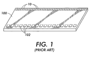
- Figure 1 is a simplified view of a photosensor array on chip.
- a chip 100 or a plurality thereof, would be used in, for example, an apparatus for recording hard-copy images, such as in a digital copier or facsimile.
- a sheet bearing an image to be recorded is moved relative to the chip and the photosensors on the chip "see,” over time, a series of small areas on the sheet, and output image signals for each small area.
- the image signals are processed and accumulated to obtain image data describing the entire recorded image.
- the chip 100 includes a linear array of photosensors; in this particular embodiment as will be described in detail below, the chip 100 includes a linear array of groups 10 of photosensors.
- Each group 10 of photosensors includes, in this embodiment, a plurality of photosensors.
- each group 10 of photosensors can effectively operate as a single, relatively large photosensor in a low-resolution mode; or, alternatively, a plurality of photosensors within each group 10 can be caused to record light and output signals independently, providing a high-resolution scan.
- the chip 100 may further include any number of contact pads 102, so the chip can interact with ancillary circuitry as desired.
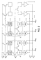
- FIG 2 is a plan, partially-schematic, view of some groups 10 of photosensors as would be found on a chip such as in Figure 1 .
- each group 10 includes a 2x2 array of photosensors, in each group marked 12a, 12b, 12c, and 12d.
- photosensors 12a, 12b in each group 10 are operable independently so that a high spatial resolution can be provided along the direction of the linear array (along the horizontal in Figure 2 ).
- the system can be operated so that every photosensor 12a, 12b, 12c, and 12d within each group 10 is, during the scanning period of "looking at" a small area in an image being recorded, connected together, by the associated transistors within each group 10, to form in effect a single large photosensor.
- operating photosensors 12a, 12b in a high-resolution mode can provide a 600 spi (spots per inch) spatial resolution
- operating all the photosensors 12a, 1 2b, 12c, and 12d in each group 10 as one photosensor provides a 300 spi spatial resolution.
- photosensors 12c and 12d in each group 10 are simply not used.
- V OV outside voltage
- ⁇ LR line readout signals
- ⁇ LR and ⁇ LR* can be connected on a single line.
- the apparatus can be operated in a "low-resolution mode," in which all of the photosensors in a group 10 in effect act as one photosensor; or in a "high-resolution mode,” in which each photosensor 12a, 12b in a group acts independently.
- the signal outputs from the photosensors are loaded into two video output lines, indicated as Vido (video odd) and Vide (video even).
- the signal outputs pass through one of a series of selectably-actuable amplifiers, PIX1, PIX2, PIX3, PIX4, etc., each of which lets a signal pass therethrough when activated.
- FIG. 3 shows a clocking sequence of inputs ⁇ PIX1 , ⁇ PIX2 , ⁇ PIX3 , and ⁇ PIX4 with regard to the associated amplifiers, which enables this odd-even output when the photosensor 12a within each group 10 sends signals to line Vido and the photosensor 12b with each group 10 sends signals to the line Vide.
- the arrangement shown in Figure 2 enables two "trains" of signals, effectively from interleaved or alternating subsets of photosensors, to be output.
- the two "trains” of signals can be multiplexed downstream to form a more directly usable video signal. Why such a two-line output arrangement is desirable is explained in the US-A-5,638,121 patent referenced above, which also teaches practical aspects of realizing such a system.
- the two-line, odd-even output system enables a faster overall output because each output signal from a photosensor must "settle” to a final value which is related to the actual amount of light energy received; the two-line system allows the settling time of adjacent odd and even photosensors to partially overlap over time as the video is output.
- the two-line, odd-even readout arrangement remains in place while the apparatus is also in its low-resolution mode, when all of the photosensors 12a, 12b, 12c, 12d in each group 10 are in effect acting together as a single photosensor.
- Figure 4 shows a clocking sequence that enables this odd-even readout in low-resolution mode, with regard to the amplifiers which control the output of signals from odd and even groups 10: in Figure 4 , it can be seen that amplifiers PIX2 and PIX3 are operated while amplifiers PIX1 and PIX 4 are not (and similarly, amplifiers that would be further to the right in Figure 2 , such as PIX6 and PIX7, not shown, would be operated while PIX5 and PIX8 are not).
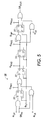
- Figure 5 is a schematic view of one embodiment of a shift register, generally indicated as 20, for operating any four amplifiers, such as PIX1, PIX2, PIX3, and PIX4 as shown in Figure 2 .
- the outputs of the shift register in Figure 5 are operational signals for the amplifiers in Figure 2 ; basically, there is one shift register stage, in the form of a flip-flop 22, corresponding to each amplifier associated with a photosensor 12a, 12b.
- the other connections to the shift register are the in and out connections SR IN and SR OUT , and a clock signal ⁇ S , as well as the line readout signals ⁇ LR and ⁇ LR* described above.
- Figures 6 and 7 are timing diagrams showing the resulting outputs to the pixel amplifiers when the apparatus is desired to be operated in high-resolution and low-resolution modes, respectively.
- all of the pixel amplifiers in the group are at one time activated within the cycle, enabling the high-resolution mode.
- only PIX2 and PIX3 are resolution mode, only one shift register stage is needed to operate each entire group 10.
- the teachings can be applied to architectures in which, for instance, four subsets of evenly-distributed photosensors or groups of photosensors output into four output lines, for an even higher-speed output.
- the two output lines could be dedicated to other types of subsets of photosensors or groups of photosensors, such as corresponding to different portions along a linear array; different linear arrays; subsets which are sensitive to different primary colors, etc.
- the above teaching is in a context of a linear array used in hard-copy scanning, the basic teachings can be applied to two-dimensional photosensor arrays, such as used in digital cameras.
Landscapes
- Engineering & Computer Science (AREA)
- Multimedia (AREA)
- Signal Processing (AREA)
- Facsimile Heads (AREA)
- Facsimile Scanning Arrangements (AREA)
Description
- The present invention relates to image sensor arrays used in raster input scanners. In particular, the invention relates to photosensitive chips wherein each photosensor has its own individual transfer circuit.
- Image sensor arrays typically comprise a linear array of photosensors which raster scan an image bearing document and convert the microscopic image areas viewed by each photosensor to image signal charges. Following an integration period, the image signal charges are amplified and transferred as an analog video signal to a common output line or bus through successively actuated multiplexing transistors. A basic circuitry for such an image sensor array is given in
U.S. Patent US-A-5,081,536 . For high-performance image sensor arrays, a preferred design includes an array of photosensors of a width comparable to the width of a page being scanned, to permit one-to-one imaging generally without the use of reductive optics. In order to provide such a "full-width" array, however, relatively large silicon structures must be used to define the large number of photosensors. A preferred technique to create such a large array is to make the array out of several butted silicon chips. In one proposed design, an array is intended to be made of 20 silicon chips, butted end-to-end, each chip having 248 active photosensors spaced at 400 photosensors per inch. - Although most scanning systems currently in use are ultimately digital systems, the "raw signal" coming out of the photosensors during the scanning process is an analog video signal, with the voltage magnitude corresponding to the intensity of light impinging on the photosensor at a given time. Thus, when signals are read out from the photosensors on a chip to be converted to digital data, different video levels are output as a series of analog voltage levels; the voltage levels each correspond to the brightness of the reflected area being scanned by a particular photosensor at a particular moment.
- The speed of output of each chip will depend on the voltage response of the output channel. A chip outputs a sequence of voltage levels, each voltage level corresponding to a pixel in the original image. With each pixel in the original image, the voltage level must move from a signal representative of light of the previous pixel to one representative of light in the present pixel. Because of the analog nature of a video-outputting chip, the sequence of voltage outputs from one voltage level (corresponding to one pixel) to the next is a set of asymptotic curves. When the outputs of a plurality of photosensors are read out serially, certain time must be allowed between each photosensor reading to allow the reading to settle to the value of a signal corresponding to the light impinging on the photosensor. In a typical practical system for reading out the video signals, this readout time for real-time scanning is approximately 50 nanoseconds per photosensor. With each pixel signal, what is of most interest is where the analog voltage curve "ends up"-- that is, the final value of the voltage signal is what is representative of the true light intensity on the photosensor. When a set of analog video signals are output over time, the "settling time" is the portion of the output for each pixel in which the voltage level starts moving from the voltage level from the previous pixel to the voltage level of the present pixel. The settling time associated with a chip directly affects the readout speed of the chip.
- A desirable feature of a photosensitive apparatus having an array of photosensors is the capability for multiple selectable imaging resolutions. For example, if a chip includes a set of photosensors spaced 600 to the inch, it may be desirable to operate the chip so that each adjacent pair of photosensors in effect operates as one photosensor, so that the effective spatial resolution of the apparatus is 300 spots per inch. A lower spatial resolution results in smaller image file sizes (which may be desirable in some scanning contexts, such as archiving, or pattern or character recognition) and can facilitate a higher readout rate. The present description relates to a photosensitive imaging apparatus which is operable at multiple resolutions.
-
WO-A- 03/034714 claim 1. -
US-A-6,377,304 describes solid-state image-pickup devices exhibiting faster video-frame processing rates, and associated methods. - It is the object of the present invention to improve an image sensor array particularly with regard to more flexible operation. This object is achieved by providing an imaging apparatus according to
claim 1 and a method of operating an imaging apparatus according to claim 7. Embodiments of the invention are sets forth in the dependant claims. -
-
Figure 1 is a simplified view of a photosensor array on a chip. -
Figure 2 is a plan, partially-schematic, view of somegroups 10 of photosensors as would be found on a chip such as inFigure 1 . -
Figures 3 and 4 show clocking sequence with regard to the inputs to the associated amplifiers shown inFigure 2 . -
Figure 5 is a schematic view of one embodiment of a shift register for operating any four amplifiers as shown inFigure 2 . -
Figures 6 and 7 are timing diagrams showing the resulting outputs to the amplifiers inFigure 2 when theFigure 5 apparatus is operated in high-resolution and low-resolution modes, respectively. -
Figure 1 is a simplified view of a photosensor array on chip. Such achip 100, or a plurality thereof, would be used in, for example, an apparatus for recording hard-copy images, such as in a digital copier or facsimile. In such an apparatus, a sheet bearing an image to be recorded is moved relative to the chip and the photosensors on the chip "see," over time, a series of small areas on the sheet, and output image signals for each small area. The image signals are processed and accumulated to obtain image data describing the entire recorded image. - In essentials, the
chip 100 includes a linear array of photosensors; in this particular embodiment as will be described in detail below, thechip 100 includes a linear array ofgroups 10 of photosensors. Eachgroup 10 of photosensors includes, in this embodiment, a plurality of photosensors. Depending on a particular selected mode of operation, eachgroup 10 of photosensors can effectively operate as a single, relatively large photosensor in a low-resolution mode; or, alternatively, a plurality of photosensors within eachgroup 10 can be caused to record light and output signals independently, providing a high-resolution scan. Thechip 100 may further include any number ofcontact pads 102, so the chip can interact with ancillary circuitry as desired. -
Figure 2 is a plan, partially-schematic, view of somegroups 10 of photosensors as would be found on a chip such as inFigure 1 . In this embodiment, eachgroup 10 includes a 2x2 array of photosensors, in each group marked 12a, 12b, 12c, and 12d. As will be described below,photosensors group 10 are operable independently so that a high spatial resolution can be provided along the direction of the linear array (along the horizontal inFigure 2 ). In a low-resolution scanning mode, however, the system can be operated so that everyphotosensor group 10 is, during the scanning period of "looking at" a small area in an image being recorded, connected together, by the associated transistors within eachgroup 10, to form in effect a single large photosensor. If operatingphotosensors photosensors group 10 as one photosensor provides a 300 spi spatial resolution. In this embodiment, whenphotosensors photosensors group 10 are simply not used. - Other inputs to the
photosensors Figure 2 include an outside voltage VOV, which is typically a constant of about 1 volt, and "line readout" signals ΦLR and its complement ΦLR*. VOV and ΦLR* can be connected on a single line. Depending on the relative values of ΦLR and its complement ΦLR*, the apparatus can be operated in a "low-resolution mode," in which all of the photosensors in agroup 10 in effect act as one photosensor; or in a "high-resolution mode," in which eachphotosensor - Further as can be seen in
Figure 2 , the signal outputs from the photosensors are loaded into two video output lines, indicated as Vido (video odd) and Vide (video even). The signal outputs pass through one of a series of selectably-actuable amplifiers, PIX1, PIX2, PIX3, PIX4, etc., each of which lets a signal pass therethrough when activated. - In this embodiment, in high-resolution mode, every other photosensor such as 12a a long the direction of the linear array sends signals to the Vido line, while the
photosensors 12b along the linear array send charges to the Vide line.Figure 3 shows a clocking sequence of inputs ΦPIX1, ΦPIX2, ΦPIX3, and ΦPIX4 with regard to the associated amplifiers, which enables this odd-even output when thephotosensor 12a within eachgroup 10 sends signals to line Vido and thephotosensor 12b with eachgroup 10 sends signals to the line Vide. In this way, the arrangement shown inFigure 2 enables two "trains" of signals, effectively from interleaved or alternating subsets of photosensors, to be output. - The two "trains" of signals can be multiplexed downstream to form a more directly usable video signal. Why such a two-line output arrangement is desirable is explained in the
US-A-5,638,121 patent referenced above, which also teaches practical aspects of realizing such a system. In brief, the two-line, odd-even output system enables a faster overall output because each output signal from a photosensor must "settle" to a final value which is related to the actual amount of light energy received; the two-line system allows the settling time of adjacent odd and even photosensors to partially overlap over time as the video is output. - Further, according to this embodiment, the two-line, odd-even readout arrangement remains in place while the apparatus is also in its low-resolution mode, when all of the
photosensors group 10 are in effect acting together as a single photosensor.Figure 4 shows a clocking sequence that enables this odd-even readout in low-resolution mode, with regard to the amplifiers which control the output of signals from odd and even groups 10: inFigure 4 , it can be seen that amplifiers PIX2 and PIX3 are operated while amplifiers PIX1 and PIX 4 are not (and similarly, amplifiers that would be further to the right inFigure 2 , such as PIX6 and PIX7, not shown, would be operated while PIX5 and PIX8 are not). ComparingFigure 4 withFigure 2 , it can be seen that signals through amplifier PIX2 (and all activated amplifiers which are even-numbered) are sent from the associatedphotosensor group 10 to line Vide, and signals through amplifier PIX3 are (and all activated amplifiers which are odd-numbered) are sent from the associatedphotosensor group 10 to line Vido. Therefore, whengroups 10 of photosensors are operated as single photosensors in a low-resolution operation, the two-train, odd-even output still applies. With this arrangement, the embodiment retains the two-line, odd-even output in both the low- and high-resolution modes. -
Figure 5 is a schematic view of one embodiment of a shift register, generally indicated as 20, for operating any four amplifiers, such as PIX1, PIX2, PIX3, and PIX4 as shown inFigure 2 . As can be seen, the outputs of the shift register inFigure 5 are operational signals for the amplifiers inFigure 2 ; basically, there is one shift register stage, in the form of a flip-flop 22, corresponding to each amplifier associated with aphotosensor Figures 6 and 7 are timing diagrams showing the resulting outputs to the pixel amplifiers when the apparatus is desired to be operated in high-resolution and low-resolution modes, respectively. InFigure 6 , when ΦLR =0 and ΦLR* =1, as can be seen, all of the pixel amplifiers in the group are at one time activated within the cycle, enabling the high-resolution mode. InFigure 7 , when ΦLR =1 and ΦLR* =0, only PIX2 and PIX3 are resolution mode, only one shift register stage is needed to operate eachentire group 10. - Although the illustrated embodiment shows the two output lines respectively dedicated to "odd" and "even" (i.e., interleaved) photosensors or groups of photosensors along a linear array, the teachings can be applied to architectures in which, for instance, four subsets of evenly-distributed photosensors or groups of photosensors output into four output lines, for an even higher-speed output. Alternatively, the two output lines could be dedicated to other types of subsets of photosensors or groups of photosensors, such as corresponding to different portions along a linear array; different linear arrays; subsets which are sensitive to different primary colors, etc. Also, although the above teaching is in a context of a linear array used in hard-copy scanning, the basic teachings can be applied to two-dimensional photosensor arrays, such as used in digital cameras.
Claims (9)
- An imaging apparatus, comprising:a plurality of groups (10) of photosensors;connection means, associated with each group of photosensors, for selectably operating the group of photosensors as effectively one photosensor such that all photosensors in each group are acting together as a single photosensor;a first output line for emitting signals from a first subset of said groups of photosensors when said connection means is active;a second output line for emitting signals from a second subset of said groups of photosensors when said connection means is active;characterized byhigh-resolution means for selectably transferring, when said connection means is not active, signals from a first photosensor (12a) of each group to the first output line, and transferring signals from a second photosensor (12b) of each group to the second output line, the first photosensor (12a) and the second photosensor (12b) being in the same group.
- The apparatus of claim 1, wherein the first subset of groups of photosensors is substantially evenly distributed along a linear array.
- The apparatus of claim 2, wherein the first subset of groups of photosensors is substantially interleaved with the second subset of groups of photosensors along the linear array.
- The apparatus of claim 1, each group of photosensors including at least two photosensors disposed along a direction of a linear array.
- The apparatus of claim 1, the connection means including at least one switch interposed between two photosensors in the group of photosensors.
- The apparatus of anyone of claims 1 to 5, the high-resolution means including a shift register having a plurality of stages, each of at least two photosensors within a group being associated with a shift register stage.
- A method of operating an imaging apparatus, the apparatus including a plurality of groups of photosensors (10), a first output line, and a second output line, comprising the steps of:providing connection means, associated with each group of photosensors, for selectably operating the group of photosensors as effectively one photosensor such that all photosensors in each group are acting together as a single photosensor; andin a first mode wherein said connection means is active, transferring a first signal from each group of a first subset of groups of photosensors to the first output line, and transferring a second signal from each group of a second subset of groups of photosensors to the second output line;characterized in thatin a second mode, wherein said connection means is not active, for each of the plurality of groups of photosensors, transferring signals from a first photosensor (12a) to the first output line, and transferring signals from a second photosensor (12b) to the second output line, the first photosensor (12a) and the second photosensor (12b) being in the same group.
- The method of claim 7, wherein the first mode corresponds to a low-resolution operation and the second mode corresponds to a high-resolution operation.
- The method of claim 7, further comprising
in the first mode, effectively connecting at least two photosensors in the group to form a single photosensor.
Applications Claiming Priority (2)
| Application Number | Priority Date | Filing Date | Title |
|---|---|---|---|
| US10/762,120 US7471327B2 (en) | 2004-01-21 | 2004-01-21 | Image sensor array with variable resolution and high-speed output |
| US762120 | 2004-01-21 |
Publications (3)
| Publication Number | Publication Date |
|---|---|
| EP1558024A2 EP1558024A2 (en) | 2005-07-27 |
| EP1558024A3 EP1558024A3 (en) | 2006-08-02 |
| EP1558024B1 true EP1558024B1 (en) | 2009-07-22 |
Family
ID=34634588
Family Applications (1)
| Application Number | Title | Priority Date | Filing Date |
|---|---|---|---|
| EP05100346A Ceased EP1558024B1 (en) | 2004-01-21 | 2005-01-20 | Image sensor array with variable resolution and high-speed output |
Country Status (6)
| Country | Link |
|---|---|
| US (1) | US7471327B2 (en) |
| EP (1) | EP1558024B1 (en) |
| JP (1) | JP2005210725A (en) |
| CN (1) | CN1645895A (en) |
| DE (1) | DE602005015498D1 (en) |
| TW (1) | TWI373263B (en) |
Families Citing this family (9)
| Publication number | Priority date | Publication date | Assignee | Title |
|---|---|---|---|---|
| JP4475665B2 (en) * | 2006-03-31 | 2010-06-09 | キヤノン株式会社 | Solid-state imaging device |
| JP5046787B2 (en) * | 2007-08-10 | 2012-10-10 | キヤノン株式会社 | Imaging system |
| JP5296417B2 (en) * | 2008-05-29 | 2013-09-25 | セイコーインスツル株式会社 | Photoelectric conversion device |
| US8212903B2 (en) * | 2009-07-31 | 2012-07-03 | Xerox Corporation | Sensor array with selectable resolution and method thereof |
| DE102010054013A1 (en) | 2010-12-10 | 2012-06-14 | Nordex Energy Gmbh | Method for operating a pitch-controlled wind turbine |
| US10145734B2 (en) * | 2016-08-22 | 2018-12-04 | Semiconductor Components Industries, Llc | Methods and apparatus for a light sensor |
| CN106331540B (en) | 2016-09-13 | 2019-09-13 | 首都师范大学 | A kind of multi-mode CMOS image sensor and its control method |
| US20230033700A1 (en) * | 2019-12-10 | 2023-02-02 | Hewlett-Packard Development Company, L.P. | Linear array of image sensor circuits including unused pixels |
| CN116132829A (en) * | 2023-01-06 | 2023-05-16 | 威海华菱光电股份有限公司 | Line array image sensor chips and image sensors |
Family Cites Families (14)
| Publication number | Priority date | Publication date | Assignee | Title |
|---|---|---|---|---|
| FR2522235B1 (en) * | 1982-02-19 | 1986-02-21 | Thomson Brandt | COLOR TELEVISION CAMERA COMPRISING A TRICHROME MATRIX FILTER |
| US5081536A (en) | 1990-12-24 | 1992-01-14 | Xerox Corporation | Image sensor array using two stage transfer having improved uniformity |
| US5493335A (en) | 1993-06-30 | 1996-02-20 | Eastman Kodak Company | Single sensor color camera with user selectable image record size |
| JP3881056B2 (en) | 1995-05-19 | 2007-02-14 | ゼロックス コーポレイション | Video image data output device |
| US6169576B1 (en) | 1996-06-18 | 2001-01-02 | Kabushiki Kaisha Toshiba | Solid state image sensing device having variable resolution and color linear image sensor having variable resolution and control method thereof |
| JP3548410B2 (en) * | 1997-12-25 | 2004-07-28 | キヤノン株式会社 | Solid-state imaging device and signal reading method of solid-state imaging device |
| US6377304B1 (en) | 1998-02-05 | 2002-04-23 | Nikon Corporation | Solid-state image-pickup devices exhibiting faster video-frame processing rates, and associated methods |
| JP2001007981A (en) * | 1999-06-23 | 2001-01-12 | Canon Inc | Photoelectric conversion device and imaging system using the same |
| JP4540280B2 (en) * | 1999-07-09 | 2010-09-08 | ベーテーエス ホールディング インターナショナル ベー ヴィ | Optical scanning device |
| EP1102323B1 (en) | 1999-11-19 | 2012-08-15 | CSEM Centre Suisse d'Electronique et de Microtechnique SA - Recherche et Développement | Method for detecting electromagnetic radiation using an optoelectronic sensor |
| JP4127942B2 (en) * | 1999-11-30 | 2008-07-30 | 株式会社東芝 | Solid-state imaging device |
| WO2002043366A2 (en) * | 2000-11-27 | 2002-05-30 | Vision Sciences Inc. | Programmable resolution cmos image sensor |
| WO2003034714A1 (en) | 2001-10-15 | 2003-04-24 | Nikon Corporation | Solid-state image pickup device |
| JP4164263B2 (en) * | 2002-01-29 | 2008-10-15 | キヤノン株式会社 | Solid-state imaging device, camera, and information processing device |
-
2004
- 2004-01-21 US US10/762,120 patent/US7471327B2/en active Active
-
2005
- 2005-01-20 JP JP2005012246A patent/JP2005210725A/en active Pending
- 2005-01-20 DE DE602005015498T patent/DE602005015498D1/en not_active Expired - Lifetime
- 2005-01-20 EP EP05100346A patent/EP1558024B1/en not_active Ceased
- 2005-01-20 CN CNA200510004297XA patent/CN1645895A/en active Pending
- 2005-01-20 TW TW094101675A patent/TWI373263B/en not_active IP Right Cessation
Also Published As
| Publication number | Publication date |
|---|---|
| US20050157192A1 (en) | 2005-07-21 |
| CN1645895A (en) | 2005-07-27 |
| TWI373263B (en) | 2012-09-21 |
| JP2005210725A (en) | 2005-08-04 |
| EP1558024A3 (en) | 2006-08-02 |
| EP1558024A2 (en) | 2005-07-27 |
| US7471327B2 (en) | 2008-12-30 |
| TW200529659A (en) | 2005-09-01 |
| DE602005015498D1 (en) | 2009-09-03 |
Similar Documents
| Publication | Publication Date | Title |
|---|---|---|
| KR101195319B1 (en) | Scanning imager using multiple chips with staggered pixels | |
| EP0809300B1 (en) | Active pixel sensor with single pixel reset | |
| JP4041695B2 (en) | Image apparatus comprising a plurality of linear photosensor arrays having different spatial resolutions | |
| JPH05167777A (en) | Multiplexing arrangement of color sensor array | |
| KR20070121837A (en) | Scanning imager using multiple chips with staggered pixels | |
| US5638121A (en) | High-speed output of video image data from an array of photosensors | |
| EP1558024B1 (en) | Image sensor array with variable resolution and high-speed output | |
| US5452001A (en) | Serial pixel readout scheme for butted sensor chips in multi-chip input scanner | |
| US6911639B2 (en) | CMOS system for capturing an image and a method thereof | |
| EP1471726B1 (en) | Image sensor array | |
| JP3581554B2 (en) | Image sensor and image reading device | |
| US20070045669A1 (en) | Image sensor | |
| US7830438B2 (en) | Frame shuttering scheme for increased frame rate | |
| EP1729504B1 (en) | System for controlling image data readout from an imaging device | |
| US6967683B2 (en) | Imaging apparatus with multiple local clocks for readout from a large number of photosensors | |
| JP3940489B2 (en) | Image reading apparatus and method | |
| US7656448B2 (en) | System for selecting a format for control data in an imaging device | |
| US20080094671A1 (en) | Image-data output system for a photosensor chip | |
| US20040246544A1 (en) | Image sensor array with multiple exposure times | |
| US7893977B2 (en) | Multiplexing and offset correction system for an image sensor array | |
| US8212903B2 (en) | Sensor array with selectable resolution and method thereof | |
| JPH0548841A (en) | Ccd line sensor | |
| JPH0946489A (en) | Image reading device |
Legal Events
| Date | Code | Title | Description |
|---|---|---|---|
| PUAI | Public reference made under article 153(3) epc to a published international application that has entered the european phase |
Free format text: ORIGINAL CODE: 0009012 |
|
| AK | Designated contracting states |
Kind code of ref document: A2 Designated state(s): AT BE BG CH CY CZ DE DK EE ES FI FR GB GR HU IE IS IT LI LT LU MC NL PL PT RO SE SI SK TR |
|
| AX | Request for extension of the european patent |
Extension state: AL BA HR LV MK YU |
|
| PUAL | Search report despatched |
Free format text: ORIGINAL CODE: 0009013 |
|
| AK | Designated contracting states |
Kind code of ref document: A3 Designated state(s): AT BE BG CH CY CZ DE DK EE ES FI FR GB GR HU IE IS IT LI LT LU MC NL PL PT RO SE SI SK TR |
|
| AX | Request for extension of the european patent |
Extension state: AL BA HR LV MK YU |
|
| 17P | Request for examination filed |
Effective date: 20061219 |
|
| 17Q | First examination report despatched |
Effective date: 20070119 |
|
| AKX | Designation fees paid |
Designated state(s): DE FR GB |
|
| GRAP | Despatch of communication of intention to grant a patent |
Free format text: ORIGINAL CODE: EPIDOSNIGR1 |
|
| RIN1 | Information on inventor provided before grant (corrected) |
Inventor name: TANDON, JAGDISH C. Inventor name: TRIPLETT, ROGER L. Inventor name: HOSIER, PAUL A. Inventor name: TEWINKLE, SCOTT L. |
|
| GRAS | Grant fee paid |
Free format text: ORIGINAL CODE: EPIDOSNIGR3 |
|
| GRAA | (expected) grant |
Free format text: ORIGINAL CODE: 0009210 |
|
| AK | Designated contracting states |
Kind code of ref document: B1 Designated state(s): DE FR GB |
|
| REG | Reference to a national code |
Ref country code: GB Ref legal event code: FG4D |
|
| REF | Corresponds to: |
Ref document number: 602005015498 Country of ref document: DE Date of ref document: 20090903 Kind code of ref document: P |
|
| PLBE | No opposition filed within time limit |
Free format text: ORIGINAL CODE: 0009261 |
|
| STAA | Information on the status of an ep patent application or granted ep patent |
Free format text: STATUS: NO OPPOSITION FILED WITHIN TIME LIMIT |
|
| 26N | No opposition filed |
Effective date: 20100423 |
|
| REG | Reference to a national code |
Ref country code: FR Ref legal event code: PLFP Year of fee payment: 12 |
|
| REG | Reference to a national code |
Ref country code: FR Ref legal event code: PLFP Year of fee payment: 13 |
|
| REG | Reference to a national code |
Ref country code: FR Ref legal event code: PLFP Year of fee payment: 14 |
|
| PGFP | Annual fee paid to national office [announced via postgrant information from national office to epo] |
Ref country code: FR Payment date: 20171221 Year of fee payment: 14 |
|
| PGFP | Annual fee paid to national office [announced via postgrant information from national office to epo] |
Ref country code: GB Payment date: 20171222 Year of fee payment: 14 |
|
| PGFP | Annual fee paid to national office [announced via postgrant information from national office to epo] |
Ref country code: DE Payment date: 20171218 Year of fee payment: 14 |
|
| REG | Reference to a national code |
Ref country code: DE Ref legal event code: R119 Ref document number: 602005015498 Country of ref document: DE |
|
| GBPC | Gb: european patent ceased through non-payment of renewal fee |
Effective date: 20190120 |
|
| PG25 | Lapsed in a contracting state [announced via postgrant information from national office to epo] |
Ref country code: FR Free format text: LAPSE BECAUSE OF NON-PAYMENT OF DUE FEES Effective date: 20190131 Ref country code: DE Free format text: LAPSE BECAUSE OF NON-PAYMENT OF DUE FEES Effective date: 20190801 |
|
| PG25 | Lapsed in a contracting state [announced via postgrant information from national office to epo] |
Ref country code: GB Free format text: LAPSE BECAUSE OF NON-PAYMENT OF DUE FEES Effective date: 20190120 |