EP1557050B1 - Dsx system mit hoher dichte - Google Patents
Dsx system mit hoher dichte Download PDFInfo
- Publication number
- EP1557050B1 EP1557050B1 EP03809546A EP03809546A EP1557050B1 EP 1557050 B1 EP1557050 B1 EP 1557050B1 EP 03809546 A EP03809546 A EP 03809546A EP 03809546 A EP03809546 A EP 03809546A EP 1557050 B1 EP1557050 B1 EP 1557050B1
- Authority
- EP
- European Patent Office
- Prior art keywords
- cross
- connect
- chassis
- termination
- jack
- Prior art date
- Legal status (The legal status is an assumption and is not a legal conclusion. Google has not performed a legal analysis and makes no representation as to the accuracy of the status listed.)
- Expired - Lifetime
Links
- 238000010618 wire wrap Methods 0.000 claims description 15
- 230000037361 pathway Effects 0.000 claims description 4
- 241000276694 Carangidae Species 0.000 description 9
- 239000000700 radioactive tracer Substances 0.000 description 5
- 238000006073 displacement reaction Methods 0.000 description 4
- 238000009413 insulation Methods 0.000 description 4
- 230000005540 biological transmission Effects 0.000 description 3
- 238000010586 diagram Methods 0.000 description 3
- 239000003989 dielectric material Substances 0.000 description 2
- 238000012360 testing method Methods 0.000 description 2
- 241000307639 Mormyrops anguilloides Species 0.000 description 1
- 241000719193 Seriola rivoliana Species 0.000 description 1
- 238000003491 array Methods 0.000 description 1
- 230000000712 assembly Effects 0.000 description 1
- 238000000429 assembly Methods 0.000 description 1
- 239000004020 conductor Substances 0.000 description 1
- 230000000977 initiatory effect Effects 0.000 description 1
- 239000000463 material Substances 0.000 description 1
- 230000013011 mating Effects 0.000 description 1
- 230000001737 promoting effect Effects 0.000 description 1
- 230000000717 retained effect Effects 0.000 description 1
- 125000006850 spacer group Chemical group 0.000 description 1
Images


Classifications
-
- H—ELECTRICITY
- H04—ELECTRIC COMMUNICATION TECHNIQUE
- H04Q—SELECTING
- H04Q1/00—Details of selecting apparatus or arrangements
- H04Q1/02—Constructional details
- H04Q1/14—Distribution frames
- H04Q1/142—Terminal blocks for distribution frames
-
- H—ELECTRICITY
- H04—ELECTRIC COMMUNICATION TECHNIQUE
- H04Q—SELECTING
- H04Q1/00—Details of selecting apparatus or arrangements
- H04Q1/02—Constructional details
- H04Q1/06—Cable ducts or mountings specially adapted for exchange installations
- H04Q1/062—Cable ducts or mountings specially adapted for exchange installations vertical management arrangements
-
- H—ELECTRICITY
- H04—ELECTRIC COMMUNICATION TECHNIQUE
- H04Q—SELECTING
- H04Q1/00—Details of selecting apparatus or arrangements
- H04Q1/02—Constructional details
- H04Q1/06—Cable ducts or mountings specially adapted for exchange installations
- H04Q1/064—Cable ducts or mountings specially adapted for exchange installations horizontal management arrangements
-
- H—ELECTRICITY
- H04—ELECTRIC COMMUNICATION TECHNIQUE
- H04Q—SELECTING
- H04Q1/00—Details of selecting apparatus or arrangements
- H04Q1/02—Constructional details
- H04Q1/09—Frames or mounting racks not otherwise provided for
-
- H—ELECTRICITY
- H04—ELECTRIC COMMUNICATION TECHNIQUE
- H04Q—SELECTING
- H04Q1/00—Details of selecting apparatus or arrangements
- H04Q1/02—Constructional details
- H04Q1/15—Backplane arrangements
- H04Q1/155—Backplane arrangements characterised by connection features
-
- H—ELECTRICITY
- H04—ELECTRIC COMMUNICATION TECHNIQUE
- H04Q—SELECTING
- H04Q1/00—Details of selecting apparatus or arrangements
- H04Q1/02—Constructional details
- H04Q1/06—Cable ducts or mountings specially adapted for exchange installations
-
- H—ELECTRICITY
- H04—ELECTRIC COMMUNICATION TECHNIQUE
- H04Q—SELECTING
- H04Q2201/00—Constructional details of selecting arrangements
- H04Q2201/12—Printed circuits
-
- H—ELECTRICITY
- H04—ELECTRIC COMMUNICATION TECHNIQUE
- H04Q—SELECTING
- H04Q2201/00—Constructional details of selecting arrangements
- H04Q2201/18—Rails
Definitions
- the present disclosure relates generally to telecommunications equipment. More particularly, the present disclosure relates to a digital cross-connect system.
- a digital cross-connect system provides a location for interconnecting two digital transmission paths.
- the apparatus for a DSX is located in one or more frames, or bays, usually in a telephone service provider's central office.
- the DSX apparatus also provides jack access to the transmission paths.
- DSX jack inserts are well known and typically include a plurality of bores sized for receiving plugs. A plurality of switches are provided adjacent the bores for contacting the plugs.
- the jack insertsw are electrically connected to digital transmission lines, and are also electrically connected to a plurality of termination members used to cross-connect the jack inserts. By inserting plugs within the bores of the jack inserts, signals transmitted through the jack inserts can be interrupted or monitored.
- FIG. 1 schematically illustrates a DSX system that is an example of the type found at a telephone service provider's central office.
- the DSX system is shown including three DSX jack inserts 10a, 10b and 10c.
- Each DSX jack insert 10a, 1O and 10c is connected to a specific piece of digital equipment.
- jack insert 10a is shown connected to digital switch 12
- jack insert 10b is shown connected to office repeater 14a
- jack insert 10c is shown connected to office repeater 14b.
- Each piece of digital equipment has a point at which a digital signal can enter, as well as a point at which the digital signal can exit.
- the jack inserts 10a, 10b and 10c each include OUT termination pins 16 and IN termination pins 18.
- the DSX jack inserts 10a, 10b and 10c are connected to their corresponding pieces of digital equipment by connecting the OUT termination pins 16 to the signals exiting the equipment (i.e., going toward the DSX system) and the IN termination pins 18 to the signals entering the equipment (i.e., going away from the DSX system).
- jack inserts 10a and 10b are "cross-connected" to one another by semi-permanent connections.
- a “semi-permanent” connection is a connection that is more permanent than the connections provided by typical patch cords equipped with tip-and-ring plugs.
- Example semi-permanent connectors include co-axial connectors, wire wrap connectors, RJ-45 type connectors and insulation displacement connectors.
- the semi-permanent connections extend between cross-connect fields 19 of the jacks inserts 10a and 10b.
- wires 20 connect OUT cross-connect pins of jack insert 10a to IN cross-connect pins of jack insert 10b.
- wires 21 connect IN cross-connect pins of jack insert 10a to OUT cross-connect pins of jack insert 10b.
- the jack inserts 10a and 10b are preferably normally closed. Thus, in the absence of a plug inserted within either of the jack inserts 10a and 10b, an interconnection is provided through the jack inserts 10a and 10b and between digital switch 12 and office repeater 14a.
- the semi-permanent connection between the digital switch 12 and the office repeater 14a can be interrupted for diagnostic purposes by inserting patch cord plugs within the IN or OUT ports of the jack inserts 10a and 10b.
- patch cords can be used to interrupt the semi-permanent connection between the jack inserts 10a and 10b to provide connections with other pieces of digital equipment.
- the digital switch 12 can be disconnected from the office repeater 14a and connected to the office repeater 14b through the use ofpatch cords 23.
- the patch cords 23 include plugs that are inserted within the IN and OUT ports of the jack 10a and the IN and OUT ports of the jack insert 10c.
- circuit density An important consideration in a digital cross-connect system is circuit density. Another important consideration is cable management. In general, improvement with regards to these and other considerations is desired.
- aspects of the present disclosure relate to high density digital cross-connect systems. At least some of the aspects assist in improving circuit densities and/or promoting cable management. These are as defined in claim 1; various preferred embodiments are detailed in the dependant claims.
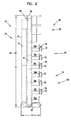
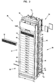
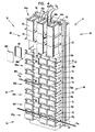
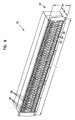
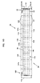
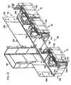
- FIGS. 2-4 illustrate a high density DSX system 30 that is one embodiment of the present disclosure.
- the DSX system 30 includes a bay 31 having a front side 52 ( FIG. 3 ) and an opposite back side 54 ( FIG. 4 ).
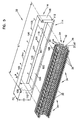
- the bay 31 is configured to hold a plurality (e.g., eighteen) of chassis 32.
- Each chassis 32 is sized to hold a plurality (e.g., twenty-one) of removable jack modules 34.
- Each of the jack modules 34 includes a jack mount 35 configured to hold a plurality (e.g., four) of jack inserts 36, 38 ( FIGS. 5 , 6 and 7 ).
- the jack modules 34 are electrically interconnected to a back plane 24 ( FIGS.
- the back plane 24 includes a rearwardly facing cross-connect field 40 and a rearwardly facing IN/OUT field 42 ( FIG. 10 ).
- the fields 40, 42 may also be referred to as panels, arrays, or blocks.
- the fields 40, 42 include a plurality of termination structures that interconnect with a cross-connect region 70 and an IN/OUT region 68, respectively (shown schematically in FIG. 11B ).
- the regions 68, 70 provide service provider interface locations at the back side 54 of the bay 31.
- the DSX system 30 defines normal-through circuits including normal through switches that provide electrical pathways between the IN/OUT field and the cross-connect field. Parts corresponding to the normal-through circuits provide means for breaking the normal-through connections between the IN/OUT and cross-connect fields to allow for signal patching and test operations. Monitor ports can also be provided.
- the chassis 32 of the DSX system 30 includes a chassis housing 100 having a front or front side 52a and a rear or back side 54a.
- a top wall 102 and a bottom wall 104 extend between the front side 52a and the back side 54a of the chassis housing 100.
- the top and bottom walls 102, 104 are interconnected by sidewalls 106, 108.
- mounting flanges 112 extend from the sidewalls 106, 108 adjacent the front side 52a of the chassis housing 100.
- the mounting flanges 112 are used to mount the chassis 32 to the bay 31 ( FIG. 3 ).
- the chassis 32 is mounted to the bay 31 such that the front side 52a of the chassis corresponds to the front side 52 of the bay 31, and the back side 54a of the chassis faces the back side 54 of the bay 31.
- the top and bottom walls 102, 104 and sidewalls 106, 108 cooperate to define an interior 110 for receiving the jack modules 34.
- the jack modules 34 mount side-by-side within the chassis 32.
- the interior 110 has a front opening 114 located adjacent the front side 52a of the housing 100 and a rear opening 116 located adjacent the back side 54a of the housing 100.
- Fasteners 101, 103 extend through upper and lower mounting strips (e.g. 119, 118 shown in FIG. 10 ) to securely fasten a back plane assembly 39 adjacent to the rear opening 116 of the chassis housing 100.
- the rear opening 116 is configured to provide rear access to the cross-connect field 40 and the IN/OUT field 42 of the back plane 24.
- the chassis 32 is adapted for housing a plurality of jack inserts, preferably at least 56 jack inserts, or 14 jack modules each having 4 jack inserts.
- the chassis 32 can have a length L1 of about 19 inches.
- An embodiment having a length L1 of about 19 inches can house, for example, 64 jack inserts, or 16 jack modules. This embodiment has a jack insert density of greater than 40 jack inserts per foot of chassis length.
- the chassis 32 could be configured to have a length L1 of about 23 inches, as shown in FIG. 6 .
- An embodiment having a length L1 of about 23 inches can house, for example, 84 jack inserts, or 21 jack modules.
- This alternative embodiment has a jack insert density of greater than 43 jack inserts per foot of chassis length.
- the chassis of the present disclosure is also configured to provide greater bay circuit density.
- the chassis has a height H1 and a depth D1.
- the height H1 is preferably less than 101.6 mm (4 inches), more preferably less than or equal to 88.9 mm (3.5 inches).
- One aspect for reducing the height as compared to prior art chassis relates to the positioning of both the IN/OUT filed and the cross-connect field at the rear of the chassis directly behind the jack modules.
- the rear access arrangement of the present disclosure reduces the overall height of the chassis and increases the stacked chassis density within the bay 31.
- the bay circuit density increases.
- the depth D1 of the chassis is between 101.6 mm and 152.4 mm (4 inches and 6 inches).
- the chassis depth D1 is equal to or less than 127 mm (5 inches).
- other sizes of chassis and other numbers of jack modules could also be used.
- the jack modules 34 of the DSX system 30 generally, includes a jack mount 35 for holding a plurality of jack inserts 36, 38, and a first circuit board section or module circuit board 130 for providing electrical connections between the jack inserts 36, 38 and the cross-connect and IN/OUT fields 40, 42 of the back plane 24 ( FIG. 5 ).
- the jack mount 35 has a front 25 and a rear 29.
- the jack inserts 36, 38 are inserted into the jack mount 35 from the front 25.
- the module circuit board 130 is positioned adjacent the rear 29 of the jack mount 35.
- each jack module 34 is preferably configured to removably receive the jack inserts 36 and 38.
- the jack inserts 36, 38 can be retained within the jack mount 35 by resilient latches 27 as described in U.S. Patent No. 6,116,961 . By flexing the latches 27, the jack inserts 36, 38 can be manually inserted into or removed from the jack mount 35.
- the jack mount 35 of each jack module 34 includes a plurality of sockets 136 and contact pins 138 (as described in U.S. Patent 6,116,961 ) for providing electrical interfaces with the jack inserts 36, 38 when the jack inserts 36, 38 are mounted in the jack mount 35.
- the contact pins 138 When assembled, the contact pins 138 are electrically connected directly to the module circuit board 130.
- the contact pins 138, or intermediate electrical conductors, interconnect the jack inserts 36, 38 to the module circuit board 130.
- jack module 34 is shown as a "four-pack" (i.e., a module including four jack inserts), it will be appreciated that alternative modules can include jack mounts sized to receive more or fewer than four jack inserts.
- the jack inserts can be mounted directly within a chassis without using separate jack mounts for holding the jack inserts.
- Further other embodiment may include different jack insert mounting configurations.
- jack inserts can be fastened within the chassis by fasteners (e.g. bolts or screws) as compared to resilient latches.
- the jack inserts include odd jack inserts 36 and even jack inserts 38. What is meant by “odd” and “even” is that the odd jack inserts 36 have access ports that are vertically offset from respective access ports of the even jack inserts 38. This configuration is designed such that when the odd and even jack inserts 36, 38 are mounted within the jack mount 35, plug bores defined by the odd and even jack inserts 36, 38 are vertically staggered relative to one another, as will be described in greater detail.
- each of the jack inserts 36, 38 includes a jack body 33; preferably the jack body is made of a dielectric material, such as plastic.
- the jack body 33 includes a front face 140 defining a plurality of access ports, in particular, an out port 148, a monitor out port 149, an in port 150 and a monitor-in port 151.
- the ports are referred to generally as 148-151.
- the subscript 'a' e.g. 148a
- the access ports 148-151 are sized to receive tip-and-ring plugs.
- the jack inserts 36, 38 also define a light emitting diode (LED) access port 152 for receiving a tracer lamp 157.
- the access ports 148-152 are accessible from the front 52a of the chassis 32 when operably positioned within the chassis ( FIG. 6 ).
- the jack inserts 36, 38 include electrical contacts 133 corresponding to each of the ports 148-151.
- the contacts 133 include tails 134 that project rearwardly from each of the jack inserts 36, 38.
- the tails 134 of the contacts 133 slide within the sockets 136 of the jack mount 34 to provide electrical connections between the module circuit board 130 and the jack inserts 36, 38.
- the jack inserts 36, 38 are removed from the jack mount 35, the jack inserts 36, 38 are electrically disconnected from the module circuit board 130 of the jack module 34.
- the front face 140 of the jack inserts 36, 38 is generally planar and defines, the out port 148, the monitor-out port 149, the in port 150, the monitor-in port 151, and the LED port 152.
- the monitor-out port 149a is spaced a first spacing S 1a from the out port 148a.
- the out port 148a is spaced a second spacing S 2a from the in port 150a.
- the in port 150a is space a third spacing S 3a from the monitor in port 151a.
- the third spacing S 3a is greater than the first spacing S 1a ; more preferably, the third spacing S 3a is greater than both the first spacing S 1a and the second spacing S 2a ; most preferably, the third spacing S 3a is greater than first spacing S 1a and the first spacing S 1a is greater than the second spacing S 2a .
- the ports 148b-152b are arranged in a different pattern than the ports 148a-152a.
- a larger spacing exists between the monitor-out port 149b and the out port 148b of even jack inserts 36 as compared to the monitor out port 149a and the out port 148a of the odd jack inserts 38.
- a reduced spacing exists between the in port 150b and the monitor-in port 151b as compared to the in port 150a and the monitor in port 151a. More specifically, the monitor-out port 149b is spaced a first spacing S 1b from the out port 148b. The out port 148b is spaced a second spacing S 2b from the in port 150b.
- the in port 150b is spaced a third spacing S 3b from the monitor-in port 151b.
- the first spacing S 1b is greater than the third spacing S 3b ; more preferably, the first spacing S 1b is greater than both the third spacing S 3b and the second spacing S 2b ; most preferably, the first spacing S 1b is greater than third spacing S 3b and the third spacing S 3b is greater than the second spacing S 2b .
- the out port 148a and the in port 150a of the odd jack inserts 36 are positioned or aligned with the first spacings S 1b of the even jack inserts 38.
- the out port 148b and the in port 150b of the even jack inserts 38 are positioned or aligned with the third spacings S 3a of the odd jack inserts 36.
- the module circuit board 130 of the jack module 34 is positioned directly behind the jack mount 35 and jack inserts 36, 38.
- the module circuit board 130 includes a major first side 131, a major second side 135, and a plurality of plated through-holes 139.
- the major first side 131 faces the front opening 114 of the chassis 32 ( FIG. 5 ) and the major second side 135 faces the rear opening 116 of the chassis.
- the plurality of plated through-holes 139 receive the contact pins 138 of the sockets 136 to provide a direct electrical connection between the module circuit board 130 and the pins 138.
- the contacts 133 of the jack inserts 36, 38 are in electrical contact with the sockets 136 and thereby also with the module circuit board 130.
- a connector 37 is electrically interconnected with tracings of the module circuit board 130 to electrically connect to the contact pins 138, and ultimately the contacts 133 of the jack inserts 36, 38.
- the connector 37 operably (i.e. electrically and mechanically) corresponds to a mating connector 47 of the back plane assembly 39 ( FIG. 9 ).
- the connectors 37 and 47 provide electrical communication between the jack module 34 and the cross-connect field 40 and the IN/OUT field 42 of the back plane assembly 39.
- the back plane 24 includes a back plane assembly 39 that mounts within the interior 110 of the chassis housing 100 adjacent to the rear opening 116.
- the jack insert modules 34 are interconnected to the back plane assembly 39 by inserting the jack insert modules 34 through the front opening 114 of the chassis housing 100.
- the modules 34 and their corresponding jack inserts are electrically connected to corresponding termination structures 44 of the cross-connect field 40 and the IN/OUT field 42.
- the back plane assembly 39 includes a second circuit board section or back plane circuit board 120 and a plurality of connectors 47.
- the back plane circuit board 120 is a single circuit board and is co-extensive with the back plane 24 of the chassis 32.
- the back plane circuit board 120 includes a major first side 121 and a major second side 123.
- the major first side 121 faces the front opening 114 of the chassis 32 ( FIG. 5 ) and the major second side 123 faces the rear opening 116 of the chassis.
- the major sides 121, 123 of the back plane circuit board 120 are generally parallel to the major sides 131, 135 of the module circuit board 130 ( FIG. 7 ).
- the back plane circuit board 120 and the module circuit board 130 are generally parallel to the back plane 24 of the system 30 ( FIG. 5 ).
- the connectors 47 are located on the major first side 121 of the back plane circuit board 120 and electrically connect each individual jack module 34 to the back plane circuit board 120.
- the back plane circuit board 120 is in turn, electrically interconnected with the cross-connect field 40 and the IN/OUT field 42.
- the back plane circuit board 120 shown in FIG. 9 includes a first array of through-holes or openings 143 and a second array of through-holes or openings 145.
- the openings 143 and 145 are plated openings configured for receipt of the termination structures 44 to provide a direct electrical connection between the back plane circuit board 120 and the structures 44.
- the termination structures 44 are directly connected to the back plane circuit board 120 through electrical connection with the openings 143 and 145.
- the termination structures include wire wrap pins/posts.
- the termination structures 44 may also include or other types of connectors/contacts for terminating a wire (e.g., insulation displacement connectors; multi-pin connectors; co-axial connectors such as BNC connectors, 1.6/5.6 connectors or SMB connectors; or RJ series connectors such as RJ45 connectors, RJ48 connectors or RJ21 connectors).
- the back plane assembly 39 includes a power source 160 that provides power to the back plane circuit board 120 and thereby to each of the individual jack modules 34.
- the power source 160 includes a ground connection, a power connection, and a sleeve ground connection. In the illustrated embodiment of FIG. 9 , the power source 160 is located above the cross-connection field 40.
- the back plane assembly 39 may include a plurality of individually sized back plane circuit boards (not shown) that are configured and sized to correspond to a single jack module 34.
- each of the individual back plane circuit boards can be electrically interconnected to a power source by a daisy chain strip.
- a spacer piece or standoff structure 166 is disposed between the back plane circuit board 120 and the module circuit boards 130 (shown in FIG. 5 ) to structurally support and properly align the jack modules 34.
- the standoff structure 166 has recesses 176 and includes three sections of structure configured to properly position and orient a plurality of jack modules 34 (e.g. seven jack modules). It is contemplated the standoff structure may also include a structure sized to position and orient any other number of jack modules, including a continuous single structure sized to position and orient twenty-one jack modules.
- the back plane assembly 39 also includes a termination member support structure 147 preferably made of a dielectric material such as plastic.
- the support structure 147 has a forward side 178 and a rearward side 180.
- the support structure 147 is divided into three support structure sections 147a, 147b, and 147c. However, a single one-piece section could also be used.
- the support structure 147 defines a first field or array of openings 153 for receiving the wire wrap pins 44 of the cross-connect field 40, and a second field or array of openings 155 for receiving the wire wrap pins 44 of the IN/OUT field 42.
- the wire wrap pins 44 are preferably press fit or staked through the openings 153, 155 and preferably have ends 154 ( FIG. 9 ) that project rearwardly from a rearward side 180 of the support structure.
- Opposite ends 156 of the pins 42 preferably terminate at the openings 143, 145 of the back plane circuit board 120 to provide an electrical connection therewith.
- the jack module 34 is inserted through the front opening 114 of the chassis 32.
- the jack module 34 is inserted rearwardly into the interior 110 of the chassis 32 until the connector 37 of the jack module engages the corresponding connector 47 that projects forwardly from the back plane assembly 39 of the chassis 32.
- the jack mounts 34 are then secured to the chassis 32.
- the jack modules can be removed from the chassis 32 by un-securing the jack mount 34 manually pulling the module 34 from the front opening 114 of the chassis 32.
- the system can be configured such that the jack inserts are inserted within the chassis directly to the back plane without the intermediate jack module 34 connection.
- the chassis itself can include integral jack mounting structure (e.g. guide or tracks) for individually receiving the jack inserts.
- the electrical contacts of the jack inserts 36, 38 include a voltage contact -48V, tracer lamp contact TL, and return contact RET corresponding to an LED circuit.
- the electrical contacts also include tip springs T and ring springs R corresponding to the monitor-in and monitor-out ports.
- the electrical contacts further include a tip-in contact TI, ring-in contact RI, cross-connect tip-in contact XTI, and cross-connect ring-in contact XRI corresponding to the in port.
- the electrical contacts further include a tip-out contact TO, ring-out contact RO, cross-connect tip-out contact XTO, and cross-connect ring-out contact XRO corresponding to the out port.
- the contacts operate in the same manner described in U.S. Patent No. 6,116,961 .
- the contacts TI, RI, XTI and XRI and the contacts TO, RO, XTO and XRO include springs that cooperate to define normally "through” or normally "closed” switches that provide electrical pathways between the cross-connect field 40 and the IN/OUT field 42 in the absence of a plug.
- the first and second circuit board sections 130, 120 include tracings 190 that electrically connect the wire wrap pins 44 of the IN/OUT field 42 to the contacts TI, RI, TO and RO of the jack inserts 36, 38.
- the circuit board sections 130, 120 also include tracings 192 that provide electrical connections between the wire wrap pins 44 of the cross-connect field 40 and contacts XTI, RTI, XTO and XRO of the jack inserts 36, 38.
- the circuit board sections 130, 120 include tracings 194 that electrically connect the tracings 190 to the MONITOR ports of the jack inserts 36, 38.
- the circuit board sections 130, 120 include tracing 196 for connecting a sleeve ground pin (not shown) to the sleeve ground contact SG of the jack inserts 36, 38; tracing 198 for connecting a tracer lamp pin of the cross-connect field 40 to the tracer lamp contacts TL of the jack inserts 36, 38; tracing 200 for connecting a power pin (not shown) to the voltage contact -48V of the jack inserts 36, 38; and tracing 202 for connecting a power return pin (not shown) to the return contact RET of the jack inserts 36, 38.
- FIG. 11B illustrates the one jack insert 36, 38 interconnected to the DSX system 30.
- the chassis 32 is arranged such that the back plane 24 faces the back side 54 of the bay 31.
- intermediate electrical connection 65 and 75 can be routed from the back plane 24 of the chassis 32 to an IN/OUT region 68 and a cross-connect region 70 located on the back side 54 of the bay 31 (see also FIG. 2 ).
- the bay 31 of the high density DSX system 30 includes a frame 50 (i.e. a rack) having a front 52, a rear 54, a top 55, and a bottom 57.
- the frame 50 has a height H measured from the bottom 57 to the top 55, a depth D measured from the front 52 to the rear 54, and a width W ( FIG. 3 ) measured between side supports 51, 53 the frame 50.
- the height H of the frame is between 2 m 13.36 cm and 3 m 65.76 cm (7 feet and 12 feet); the depth D is between 381 mm and 482.6 mm (15 and 19 inches); and the width W is between 558.8 mm and 762 mm (22 and 30 inches).
- the height H is often about 9 to 11 feet; the depth D is about 18.75 inches; and the width W is about 26 inches.
- the height H is about 2.2 m; the depth D is about 746 mm; and the width W is about 600 mm.
- the system 30 is arranged such that the IN/OUT fields 42 are electrically connected to the IN/OUT region 68.
- the IN/OUT region 68 is positioned in an upper region 56 at the rear 54 of the bay 31.
- the cross-connect fields 42 are electrically connected to the cross-connect region 70.
- the cross-connect region 70 is located in a lower region 58 at the rear 54 of the bay 31.
- the front 52 of the bay 31 is configured to receive the plurality of the chassis 32.
- Each chassis 32 is secured to the bay 31 at mounting structure 41, 43 located adjacent the side supports 51, 53 of frame 50.
- the chassis 32 can be mounted to the frame 50 of the bay 31 using conventional fasteners.
- the mounting flanges 112 ( FIG. 5 ) of the chassis 32 mount to forward facing surfaces 81, 83 of the mounting structure 41, 43.
- the forward facing surfaces 81, 83 may also be used to attach or adhere labels that identify the individual chassis 32.
- hinged panels or doors, 48 are located on the mounting structures 41, 43 to cover the forward facing surfaces 81, 83 and provide additional area upon which identification material can be located.
- the plurality of chassis 32 of the present system 30 typically includes about 14-21 chassis, preferably 18 chassis.
- the system 30 is configured to accommodate 84 circuits (21 jack modules each having 4 jack inserts) at each chassis for a system total of 1512 circuits (18 chassis each having 84 cross connection circuits).
- chassis sizes and bay sizes are contemplated.
- the chassis 32 and the bay 31 provide an increased circuit density not previously provided by conventional systems, to effectively and efficiently manage of a mass number of digital circuits.
- the IN/OUT region 68 located in the upper region 56 of the bay 31 includes a plurality of IN/OUT wire termination blocks 62.
- Each IN/OUT termination block includes a termination panel 69.
- the termination blocks 62 are mounted to a frame backing 620 by a bracket 622.
- the frame backing 620 is secured to the rear or back side 54 of the frame 50 ( FIG. 4 ).
- the blocks 62 are arranged in a plurality of columns 64 (e.g. 3 vertical columns 64a-64c).
- Vertical IN/OUT cable management channels 66 i.e. channels 66a and 66b are defined between the columns 64 of termination blocks 62.
- the cables C IO are routed from the ceiling of the surrounding area.
- the cables C IO enter the top 55 of the bay 31, are routed through the vertical IN/OUT cable management channels 66, and terminate at the termination panels 69 of the IN/OUT region 68.
- the cables C IO are routed within the vertical IN/OUT cable management channels 66 and can be directed to either column of blocks 62 (i.e. 64a or 64b and 64b or 64c) defining the vertical channel 66.
- a block 62 located in the central vertical column 64b can thereby have a first terminating cable C IO that is routed within a first vertical channel (e.g. 66a) and a second terminating cable C IO that is routed within a second vertical channel (e.g. 66b).
- the cables C IO can be routed from a raised floor and enter the bay 31 from the bottom 57.
- the IN/OUT region 68 can be located in the lower region 58 of the bay 31 and the cross-connect region 70 can be located in the upper region 56.
- the IN/OUT field 42 of each chassis 32 is electrically connected to a corresponding termination panel 69 of the IN/OUT region 68 by the interconnect or intermediate IN/OUT cable 65, shown schematically in FIG. 11B .
- two chassis are connected to each of the termination blocks 62.
- the intermediate IN/OUT cables 65 are routed from the IN/OUT field 42 of the back plane 24 of the chassis 32 through cable passages 680 and 682 ( FIG. 12 ) in the frame backing 620 and bracket 622.
- each of the IN/OUT termination panels 69 includes a front side 602, a rear side 604, and a plurality of termination members 612.
- the termination members 612 include wire wrap pins or posts that are mounted within an array of holes 610 extending through the panel 69. More specifically, the termination members 612 have a front end or portion 616 that extends from the front side 602 of the termination panel 69 and a rear end or portion 618 that extends from the rear side 604 of the panel 69. (For clarity, only a few termination members 612 are shown in FIG. 12 and the termination members are omitted from FIG. 4 . It will be appreciated that in actual use, a termination member 612 will be staked through each of the holes 610 of the panel 69. The termination members 612 are shown schematically in FIG. 11A .)
- the termination members 612 may also include or other types of connectors/contacts for terminating a wire (e.g., insulation displacement connectors; multi-pin connectors; co-axial connectors such as BNC connectors, 1.6/5.6 connectors or SMB connectors; or RJ series connectors such as RJ45 connectors, RJ48 connectors or RJ21 connectors).
- a wire e.g., insulation displacement connectors; multi-pin connectors; co-axial connectors such as BNC connectors, 1.6/5.6 connectors or SMB connectors; or RJ series connectors such as RJ45 connectors, RJ48 connectors or RJ21 connectors.
- the IN/OUT termination panels 62 preferably include at least one cable management device 628.
- the cable management device 628 can include, for example, tie down bars, rings, fingers, loops, brackets, or punch-out areas.
- the cable management device 628 includes a fanning strip 630, more preferably, a first fanning strip 630 and a second fanning strip 632 to separate and organize wires of the equipment cable C IO that terminate on the termination panels 69.
- the termination blocks 62 may include hinged covers 650 ( FIG. 4 ) to cover and protect the termination members 612 extending from the rear side 604 of the panels 69.
- the cover 650 is arranged to pivot about hinges at either the first or second fanning strips 630, 632 ( FIG. 12 ) to provide access to cables positioned in either of the fanning strips 630, 632.
- the covers are removable from the IN/OUT termination panels 62 and include snap-fit hinges for ease of assembly and access to the covered termination members 612.
- the cross-connect region 70 located in the lower region 58 of the bay 31 includes a plurality of cross-connect wire termination blocks 72.
- Each cross-connect termination block 72 includes a cross-connect termination panel 74 (see FIG. 13 ).
- the plurality of cross-connect termination blocks 72 are arranged in rows 80 (e.g. 6 horizontal rows 80a-80g).
- Horizontal cross-connect cable management channels 78 i.e. horizontal channels 78a-78g
- the horizontal cross-connect channels 78 receive cables C XC from other bays that terminate at cross-connect blocks 72 of the cross-connect region 70.
- a cross-connect termination region 70 is described in U.S. Patent 5,220,600 (shown partially in FIG. 13 of the present disclosure).
- a vertical cross-connect cable management channel 88 is forwardly offset from the horizontal cross-connect cable management channels 78(a-g).
- the vertical cross-connect cable management channel 88 allows cables to be routed from one horizontal cross-connect channel, e.g. 78a, to another horizontal cross-connect channel, e.g. 78d.
- the cables within the cross-connect termination region 70 are contained within the frame 50 and do not have to be routed along an exterior side of the frame.
- Access gaps or openings 86 are provided in the horizontal rows 80 between the connector blocks 72. The access openings 86 assist a user in routing cables from the vertical cross-connect cable management channel 88 to one of the horizontal cross-connect channel 78a-78g, and vise versa.
- each chassis 32 is electrically connected to a corresponding cross-connect termination panel 74 of the cross-connect region 70 by the interconnect or intermediate cross-connect cable 75, shown schematically in FIG. 11B .
- each chassis 32 is connected to a single corresponding connector block 72.
- the intermediate cross-connect cable 75 is routed from the cross-connect field 40 of the back plane 24 of the chassis 32 through openings 720 ( FIG. 13 ).
- the openings 720 are essentially the open regions of the frame 50 where no horizontal channel 78 structures extend.
- the intermediate cross-connect cables 75 are routed directly through the frame to a horizontal cross-connect cable management channel 78 located approximately adjacent to the chassis 32. From there, the intermediate cross-connect cable 75 can be routed to a cross-connect termination block 70 associated with the particular horizontal channel, or routed to the vertical cross-connect channel 88 to another horizontal cross-connect cable management channel 78.
- each of the cross-connect termination panels 74 includes a front side 702, a rear side 704 and termination members 712.
- the termination members 712 include wire wrap pins or posts that are mounted within an array of holes (not shown) extending through the panel 74. More specifically, the termination members 712 have a front end or portion 716 that extends from the front side 702 of the termination panel 74 and a rear end or portion 718 that extends from the rear side 704 of the panel 74.
- the intermediate cables 75 interconnect the front portions 716 of the termination members 712 of the cross-connect block 72 and the rear portion 154 of wire wrap pins 44 of the back plane 24 (i.e. of the cross-connect field 40).
- the termination members 712 may also include or other types of connectors/contacts for terminating a wire (e.g., insulation displacement connectors; multi-pin connectors; co-axial connectors such as BNC connectors, 1.6/5.6 connectors or SMB connectors; or RJ series connectors such as RJ45 connectors, RJ48 connectors or RJ21 connectors).
- a wire e.g., insulation displacement connectors; multi-pin connectors; co-axial connectors such as BNC connectors, 1.6/5.6 connectors or SMB connectors; or RJ series connectors such as RJ45 connectors, RJ48 connectors or RJ21 connectors.
- Each cross-connect termination panel 74 is mounted to the lower region 58 of the frame 50 by a mounting bracket 722.
- the mounting bracket 722 is mounted to a generally L-shaped bracket 724 having a vertical plate 726 and a horizontal plate 728.
- the vertical plate 726 and the horizontal plate 728 generally define the horizontal cross-connect cable management channel 78.
- Side plates 730 can be positioned adjacent each particular termination blocks 72 that have exposed sides to protect the electrical wire connections extending from the front sides 702 of the panels 74.
- a cover 750 is provided to protect the rear portions 718 of the termination members 712.
- the cover 750 is pivotally attached to the mounting bracket 722.
- the cover 750 can be configured to pivot upward to access the termination members 712, as shown in FIG. 13 ; or configured to pivot downward to access the termination member 712, as shown in FIG. 14 .
- a retaining structure 752 selectively retains the cover 750 is an open position.
- another retaining structure 754 selectively retains the cover 750 in a closed position.
- cables C IO ( FIG. 4 ) from separate pieces of equipment enter at the top 55 of the frame 50 and run within the vertical IN/OUT cable management channels 66 of the IN/OUT region 68.
- the equipment cables C IO are positioned within the fanning strips 630, 632 ( FIG. 12 ) and terminated at the rear side 604 of a particular termination panel 69.
- Each of the termination blocks 62 is connected to the back plane 24 of up to two corresponding chassis 32 by the intermediate IN/OUT cables 65.
- the intermediate IN/OUT cables 65 extends from the front side 602 of the termination panel 69 to the corresponding IN/OUT field 42 of the corresponding chassis 32.
- the IN/OUT field 42 is in electrical communication with the cross-connect field 40 (e.g. by DSX switching circuitry).
- the cross-connect field 40 of the chassis 32 is interconnected to a corresponding connector block 72 by an intermediate cross-connect cable 75.
- the intermediate cross-connect cable 75 extends from the cross-connect field 42 of the chassis 32 to the front side 702 of the corresponding cross-connect panel 74 ( FIG. 14 ). Cables Cxc ( FIG. 4 ) from other bays, routed within the horizontal cross-connect channels 78 (and vertical cross-connect channel 88) terminate at the rear side 704 of the termination panel 74 (i.e. terminate at the rear portion 718 of the termination members 712).
- the cable management arrangement of the bay 31 is such that the IN/OUT cables C IO enter at the top of the frame to eliminate side entrances so that additional bays can be positioned in a close side-by-side arrangement.
- the cables C IO run along the vertical IN/OUT channels 66 to termination at an IN/OUT termination block 62.
- the intermediate IN/OUT cables 65 are contained solely within the frame 50.
- the intermediate cross-connect cables 75 are also contained solely within the frame 50.
- the cable management arrangement of the bay 31 is further configured such that horizontal channels 78a-78g are in horizontal alignment with other bays positioned in close side-by-side relation.
- the cross-connect cables C XC can be routed freely in a horizontal manner from one bay to another.
- the cables C XC are not obstructed and can be diverted or routed to the vertical channel 88 or a cross-connect termination panel 71 in an organized manner.
- the DSX system 30 is utilized in the same manner as a conventional DSX system.
- the IN/OUT blocks 42 allow the jacks 36, 38 to be connected to pieces of digital equipment.
- the cross-connect blocks 40 allow the jacks 36, 38 to be cross-connected by semi-permanent jumpers.
- the jacks 36, 38 provide normally-through circuits between the digital equipment connected to the IN/OUT blocks 42 and the cross-connect blocks 40.
- the tracer lamp circuits allow the cross-connected jacks being monitored to be traced as is described in U.S. Patent No. 6,116,961 . Plugs can be inserted in the IN or OUT ports of the jacks 36, 38 for testing or diagnostic purposes, or for re-routing signals to different pieces of digital equipment.
Landscapes
- Engineering & Computer Science (AREA)
- Computer Networks & Wireless Communication (AREA)
- Structure Of Telephone Exchanges (AREA)
- Signal Processing For Digital Recording And Reproducing (AREA)
- Lubricants (AREA)
- Optical Communication System (AREA)
- Gas Separation By Absorption (AREA)
- Treating Waste Gases (AREA)
- Multi-Conductor Connections (AREA)
Claims (17)
- Telekommunikationsvorrichtung, die folgendes aufweist:ein Gestell (50), das eine Vorderseite (52) und eine Rückseite (54) hat;eine Vielzahl von Einschüben (32), die an der Vorderseite des Gestells (52) angebracht sind, wobei jeder Einschub (32) eine Vorderseite (52a) und eine Rückseite (54a) hat, gekennzeichnet durch:wobei das Gestell (50) vertikale EIN/AUS-Kabelführungskanäle (66) aufweist, die zwischen den vertikalen Spalten von EIN/AUS-Anschlussplatten (69) positioniert sind, um EIN/AUS-Kabel (65) zu führen, die mit den Rückseiten (604) der EIN/AUS-Anschlussplatten (69) gekoppelt sind;jeder Einschub (32) hat jeweils eine Höhe von weniger als 101,6 mm (4 inches);eine Vielzahl von Einsätzen (36, 38), die in den Einschüben (32) angebracht sind, wobei die Einsätze (36, 38) Anschlüsse (148-151) aufweisen, die zur Aufnahme von Steckern ausgebildet sind, wobei die Einsätze (36, 38) Normaldurchgangsschalter aufweisen, die Kopf- und Umfangsfedern zum Kontakt mit den Steckern haben, wenn die Stecker in die Anschlüsse (148-151) eingesetzt sind, wobei die Normaldurchgangsschalter außerdem Normalfedern aufweisen, die mit den Kopf- und Umfangsfedern in Eingriff sind, wenn die Stecker nicht in die Anschlüsse (148-151) eingesetzt sind, wobei die Anschlüsse (148-151) von der Vorderseite (52a) der Einschübe (32) zugänglich sind und wobei die Einsätze (36, 38) mit einer Dichte von mindestens 40 Einsätzen (36, 38) pro Fuß der Einschub(32)-Breite angeordnet sind;Crossconnect-Anschlussstrukturen (40), die an der Rückseite (54a) der Einschübe (32) positioniert sind;EIN/AUS-Anschlussstrukturen (42), die an der Rückseite (54a) der Einschübe (32) positioniert sind;Normaldurchgangsschaltkreise, welche die EIN/AUS-Anschlussstrukturen (42) jedes Einschubs (32) mit den entsprechenden Crossconnect-Anschlussstrukturen (40) jedes Einschubs verbinden, wobei die Normaldurchgangsschaltkreise die Normaldurchgangsschalter aufweisen;EIN/AUS-Anschlussplatten (69), die an der Rückseite (54) des Gestells (50) angebracht sind, wobei die EIN/AUS-Anschlussplatten (69) Vorderseiten (602) und Rückseiten (604) aufweisen, die EIN/AUS-Anschlussplatten (69) in einer Vielzahl von vertikalen Spalten angeordnet sind, und die EIN/AUS-Anschlussplatten (69) mit den EIN/AUS-Anschlussstrukturen (42) der Einschübe (32) elektrisch verbunden sind durch erste Verbindungskabel (65), die durch das Gestell (50) von den EIN/AUS-Anschlussstrukturen (42) zu den Vorderseiten der EIN/AUS-Anschlussplatten (69) verlaufen;Crossconnect-Anschlussplatten (74), die an der Rückseite des Gestells (50) angebracht sind, wobei die Crossconnect-Anschlussplatten (74) Vorderseiten (702) und Rückseiten (704) aufweisen, die Crossconnect-Anschlussplatten (74) in einer Vielzahl von horizontalen Reihen angeordnet sind, und die Crossconnect-Anschlussplatten mit den Crossconnect-Anschlussstrukturen (490) der Einschübe elektrisch verbunden sind durch zweite Verbindungskabel (75), die durch das Gestell (50) von den Crossconnect-Anschlussstrukturen (40) zu den Vorderseiten (702) der Crossconnect-Anschlussplatten (74) verlaufen;
wobei das Gestell (50) horizontale Crossconnect-Kabelführungskanäle (78) entsprechend mindestens einigen der horizontalen Reihen von Crossconnect-Anschlussplatten (74) aufweist, um Crossconnect-Kabel (75) zu führen, die mit den Rückseiten (704) der Crossconnect-Anschlussplatten (78) gekoppelt sind; und
wobei das Gestell (50) mindestens einen vertikalen Crossconnect-Kabelführungskanal (88) hat, der von den horizontalen Crossconnect-Kabelführungskanälen (78) nach vorne versetzt ist, wobei das Gestell (50) außerdem Kabelanschlussöffnungen (720) aufweist, um das Leiten von Crossconnect-Kabeln (75) von dem vertikalen Crossconnect-Kabelführungskanal (88) zu den horizontalen Crossconnect-Kabelführungskanälen (78) zu ermöglichen. - Telekommunikationsvorrichtung nach Anspruch 1, wobei die Normaldurchgangsschaltkreise elektrische Bahnen haben, die von ersten (120) und zweiten (130) Leiterplattenabschnitten gebildet sind, die miteinander elektrisch verbunden sind, wobei der erste Leiterplattenabschnitt (120) hinter den Einsätzen (36, 38) und vor dem zweiten Leiterplattenabschnitt (130) positioniert ist, der zweite Leiterplattenabschnitt (130) vor den Crossconnect-Anschlussstrukturen (40) und den EIN/AUS-Anschlussstrukturen (42) positioniert ist, die ersten (120) und die zweiten (130) Leiterplattenabschnitte jeweils eine erste Hauptseite (121, 131) und eine zweite Hauptseite (123, 133) aufweisen, wobei die ersten Hauptseiten (121, 131) in eine Vorwärtsrichtung weisen und die zweiten Hauptseiten (123, 133) in eine Rückwärtsrichtung weisen.
- Telekommunikationsvorrichtung nach Anspruch 2, wobei die EIN/AUS-Anschlussstrukturen (42) und die Crossconnect-Anschlussstrukturen (40) mechanisch und elektrisch direkt mit dem zweiten Leiterplattenabschnitt (130) verbunden sind.
- Telekommunikationsvorrichtung nach Anspruch 2 oder 3, wobei die EIN/AUS-Anschlussstrukturen (42) und die Crossconnect-Anschlussstrukturen (40) Leitungswickelelemente aufweisen.
- Telekommunikationsvorrichtung nach einem der vorhergehenden Ansprüche, wobei die Normaldurchgangsschaltkreise elektrische Bahnen aufweisen, die von mindestens einer Leiterplatte für jeden Einschub (32) gebildet sind, wobei die Leiterplatten angrenzend an Rückwände der Einschübe (32) positioniert sind.
- Telekommunikationsvorrichtung nach einem der vorhergehenden Ansprüche, wobei die EIN/AUS-Anschlussstrukturen (42) und die Crossconnect-Anschlussstrukturen (40) Leitungswickelelemente aufweisen, die unmittelbar mit den Leiterplatten (130) verbunden sind.
- Telekommunikationsvorrichtung nach einem der vorhergehenden Ansprüche, die ferner mindestens eine Leiterplatte (120) entsprechend jedem der Einschübe (32) aufweist, wobei die Leiterplatten (120) jeweils eine in eine Vorwärtsrichtung weisende erste Hauptseite (121) und eine in eine Rückwärtsrichtung weisende zweite Hauptseite (123) haben, wobei die EIN/AUS-Anschlussstrukturen (42) und die Crossconnect-Anschlussstrukturen (40) Leitungswickelelemente aufweisen, die von den zweiten Hauptseiten (123) der Leiterplatten nach rückwärts vorstehen.
- Telekommunikationsvorrichtung nach einem der vorhergehenden Ansprüche, wobei die Höhe jedes Einschubs (32) kleiner oder gleich 88,9 mm (3,5 inches) ist.
- Telekommunikationsvorrichtung nach einem der vorhergehenden Ansprüche, wobei jeder Einsatz (36, 38) zwei Überwachungsports aufweist.
- Telekommunikationsvorrichtung nach einem der vorhergehenden Ansprüche, wobei jeder Einschub (32) mindestens 84 der Einsätze hält.
- Telekommunikationsvorrichtung nach einem der vorhergehenden Ansprüche, wobei das Gestell (50) mindestens 18 der Einschübe (32) haltert.
- Telekommunikationsvorrichtung nach einem der vorhergehenden Ansprüche, wobei mindestens einige Einsätze (36, 38) mit einer Dichte von mindestens 43 Einsätzen (36, 38) pro Fuß der Einschubbreite angeordnet sind.
- Telekommunikationsvorrichtung nach einem der vorhergehenden Ansprüche, wobei Einsätze (36, 38) mit einer Dichte von mindestens 43 Einsätzen (36, 38) pro 304,8 mm (Fuß) der Einschub-(32)-Breite angeordnet sind.
- Telekommunikationsvorrichtung nach einem der vorhergehenden Ansprüche, wobei
die Einsätze (36, 38) jeweils einen dielektrischen Körper aufweisen, in dem die Kopf-Federn, die Umfangs-Federn und die Normalfedern angebracht sind, wobei der dielektrische Körper ein Vorder- und ein Hinterende aufweist, das Vorderende die Anschlussports (148-151) definiert und die Federn Endstücke aufweisen, die von dem Hinterende des dielektrischen Körpers nach hinten vorstehen. - Telekommunikationsvorrichtung nach einem der vorhergehenden Ansprüche, wobei die EIN/AUS-Anschlussstrukturen (42) und die Crossconnect-Anschlussstrukturen (40) direkt an die Leiterplatten (120, 130) angeschlossen sind.
- Telekommunikationsvorrichtung nach einem der vorhergehenden Ansprüche, wobei
mindestens einer der vertikalen EIN/AUS-Kabelführungskanäle (66) den Zugang zu mehr als einer vertikalen Spalte von EIN/AUS-Anschlussplatten (69) vorsieht. - Telekommunikationsvorrichtung nach einem der vorhergehenden Ansprüche, wobei mindestens eines der EIN/AUS-Anschlussplatten (69), die mit der Rückseite (604) gekoppelte EIN/AUS-Kabel (65) haben, folgendes hat: ein erstes EIN/AUS-Kabel (65), das in einem ersten vertikalen EIN/AUS-Kabelführungskanal (66) positioniert ist und an der Rückseite der Platte (130) abgeschlossen ist, und ein zweites EIN/AUS-Kabel (65), das in einem zweiten vertikalen EIN/AUS-Kabelführungskanal (66) positioniert ist und an der Rückseite der Platte (130) abgeschlossen ist.
Applications Claiming Priority (3)
| Application Number | Priority Date | Filing Date | Title |
|---|---|---|---|
| US277174 | 2002-10-18 | ||
| US10/277,174 US7095844B2 (en) | 2002-10-18 | 2002-10-18 | High density DSX system |
| PCT/US2003/031996 WO2004039094A2 (en) | 2002-10-18 | 2003-10-08 | High density dsx system |
Publications (2)
| Publication Number | Publication Date |
|---|---|
| EP1557050A2 EP1557050A2 (de) | 2005-07-27 |
| EP1557050B1 true EP1557050B1 (de) | 2008-07-16 |
Family
ID=32093219
Family Applications (1)
| Application Number | Title | Priority Date | Filing Date |
|---|---|---|---|
| EP03809546A Expired - Lifetime EP1557050B1 (de) | 2002-10-18 | 2003-10-08 | Dsx system mit hoher dichte |
Country Status (10)
| Country | Link |
|---|---|
| US (2) | US7095844B2 (de) |
| EP (1) | EP1557050B1 (de) |
| CN (1) | CN100551089C (de) |
| AT (1) | ATE401745T1 (de) |
| AU (1) | AU2003277327A1 (de) |
| BR (1) | BR0315410A (de) |
| DE (1) | DE60322246D1 (de) |
| MX (1) | MXPA05004035A (de) |
| TW (1) | TWI348308B (de) |
| WO (1) | WO2004039094A2 (de) |
Families Citing this family (22)
| Publication number | Priority date | Publication date | Assignee | Title |
|---|---|---|---|---|
| US7095844B2 (en) * | 2002-10-18 | 2006-08-22 | Adc Telecommunications, Inc. | High density DSX system |
| US20060067068A1 (en) * | 2004-09-27 | 2006-03-30 | Petersen Cyle D | Digital cross-connect system and rack arrangement |
| DE102005022547B4 (de) * | 2005-05-18 | 2008-07-03 | Adc Gmbh | Verteilereinrichtung im Teilnehmeranschlussbereich |
| DE102005022689B4 (de) * | 2005-05-18 | 2007-09-20 | Adc Gmbh | Aktive Verteilereinrichtung im Teilnehmeranschlussbereich |
| US20070211740A1 (en) * | 2006-03-07 | 2007-09-13 | Jorg Franzke | Telecommunications distribution system with line sharing |
| US20070211882A1 (en) * | 2006-03-07 | 2007-09-13 | Francois Hatte | Control method for a telecommunication distribution system |
| US20070211883A1 (en) * | 2006-03-07 | 2007-09-13 | Jorg Franzke | Telecommunications device having distribution units arranged in block configuration |
| US8437344B2 (en) * | 2006-03-07 | 2013-05-07 | Adc Telecommunications, Inc. | Telecommunication distribution device with multi-circuit board arrangement |
| US8395199B2 (en) | 2006-03-25 | 2013-03-12 | 4D-S Pty Ltd. | Systems and methods for fabricating self-aligned memory cell |
| US7889516B2 (en) * | 2007-05-22 | 2011-02-15 | At&T Intellectual Property I, L.P. | Cable management system with inspection window |
| US7787260B2 (en) * | 2007-07-09 | 2010-08-31 | Adc Telecommunications, Inc. | Cable management arrangement for a telecommunications cabinet |
| US8289717B2 (en) * | 2007-07-19 | 2012-10-16 | Qwest Communications International Inc. | Protective telecommunications enclosure systems and methods |
| US8867234B2 (en) * | 2007-07-19 | 2014-10-21 | Qwest Communications International Inc. | Protective telecommunications enclosure systems and methods |
| US9095045B2 (en) * | 2007-07-19 | 2015-07-28 | Centurylink Intellectual Property Llc | Protective telecommunications enclosure systems and methods |
| US20090227123A1 (en) * | 2008-03-07 | 2009-09-10 | Tellabs Bedford, Inc. | Connectorized alarm cross connect panel |
| US20110103575A1 (en) * | 2009-10-30 | 2011-05-05 | Telect Inc. | High-density splitter/patch telecommunications system |
| US20110210654A1 (en) * | 2010-02-26 | 2011-09-01 | Qwest Communications International Inc. | Tippable shelf for telecommunications rack |
| US9521766B2 (en) | 2012-06-27 | 2016-12-13 | CommScope Connectivity Belgium BVBA | High density telecommunications systems with cable management and heat dissipation features |
| US9285557B2 (en) | 2012-06-27 | 2016-03-15 | Tyco Electronics Raychem Bvba | High density telecommunications chassis with cable management |
| FR3076177B1 (fr) * | 2017-12-22 | 2021-03-26 | Bull Sas | Systeme d'interconnexion de cartes electroniques et armoire de calcul informatique comprenant un tel systeme |
| FR3080496B1 (fr) * | 2018-04-23 | 2020-05-15 | Schneider Electric Industries Sas | Module intelligent pour panneau d'armoire de brassage recevant des cables de transfert de donnees |
| CN111653904B (zh) * | 2020-05-28 | 2021-11-09 | 南京普天天纪楼宇智能有限公司 | 一种带有智能芯片管理功能的rj45接口连接器 |
Family Cites Families (40)
| Publication number | Priority date | Publication date | Assignee | Title |
|---|---|---|---|---|
| US3852703A (en) * | 1973-01-05 | 1974-12-03 | Porta Syst | Modular jack strip assembly |
| US4722702A (en) * | 1982-06-14 | 1988-02-02 | Porta Systems Corp. | High density front administered protector block |
| US4548453A (en) * | 1983-03-11 | 1985-10-22 | Amp Incorporated | Right angle coaxial plug connector |
| US4603377A (en) * | 1983-10-24 | 1986-07-29 | Nec Corporation | Main distributing frame board for an electronic switching system |
| US4665546A (en) * | 1985-03-13 | 1987-05-12 | Reliance Comm/Tec Corporation | Modular distribution frame assembly |
| US4749968A (en) * | 1985-12-13 | 1988-06-07 | Adc Telecommunications, Inc. | Jack device |
| US4649236A (en) * | 1985-12-23 | 1987-03-10 | Porta Systems Corp. | Digital system connect frame |
| US4737985A (en) * | 1986-10-31 | 1988-04-12 | Porta Systems Corp. | Digital system connect frame |
| US4820200A (en) * | 1987-02-13 | 1989-04-11 | Switchcraft, Inc. | Slab-like jack module |
| US4770639A (en) * | 1987-03-02 | 1988-09-13 | Switchcraft, Inc. | Channelized jackfield |
| US4840568A (en) * | 1987-03-31 | 1989-06-20 | Adc Telecommunications, Inc. | Jack assembly |
| US4861281A (en) * | 1988-09-01 | 1989-08-29 | Telect, Inc. | Electrical jack unit |
| US4911661A (en) * | 1989-04-14 | 1990-03-27 | Porta Systems Corp. | Hinged cover for telephone connector blocks |
| US5220600A (en) * | 1989-11-14 | 1993-06-15 | Adc Telecommunications, Inc. | High-density cross-connect bay |
| US4975087A (en) * | 1989-12-18 | 1990-12-04 | Telect, Inc. | Telecommunication bantam jack module |
| US5145416A (en) * | 1989-12-19 | 1992-09-08 | Adc Telecommunications, Inc. | Jack assembly |
| US5170327A (en) * | 1990-11-05 | 1992-12-08 | Adc Telecommunications, Inc. | Distal distribution frame module |
| US5199878A (en) * | 1990-11-15 | 1993-04-06 | Adc Telecommunications, Inc. | Plug-in jack card for normally closed contacts |
| US5078624A (en) * | 1991-05-28 | 1992-01-07 | Adc Telecommunications, Inc. | Digital signal cross-connect module |
| US5233501A (en) * | 1992-02-27 | 1993-08-03 | Telect, Inc. | Digital telecommunication network cross-connect module having a printed circuit board connected to jack switches |
| DE69220244T2 (de) * | 1992-04-02 | 1997-09-25 | Adc Telecommunications, Inc., Minneapolis, Minn. | Miniatur-koaxialklinkensteckvorrichtung |
| AU5296993A (en) * | 1992-10-05 | 1994-04-26 | Adc Telecommunications, Incorporated | Jack module assembly |
| US5393249A (en) * | 1993-06-30 | 1995-02-28 | Adc Telecommunications, Inc. | Rear cross connect DSX system |
| US5417588A (en) * | 1993-11-15 | 1995-05-23 | Adc Telecommunications, Inc. | Coax connector with center pin locking |
| US5634822A (en) * | 1994-11-14 | 1997-06-03 | Augat Inc. | Miniature telephone jack and rack system |
| US5738546A (en) * | 1994-12-01 | 1998-04-14 | Adc Telecommunications, Inc. | Printed circuit board mounted jack |
| US5546282A (en) * | 1995-05-02 | 1996-08-13 | Telect, Inc. | Telecommunication network digital cross-connect panels having insertable modules with printed circuit board mounted coaxial jack switches |
| WO1996038884A1 (en) | 1995-05-31 | 1996-12-05 | Telect, Inc. | Telecommunication jack module with interchangeable back plane |
| US5685741A (en) * | 1996-06-27 | 1997-11-11 | Adc Telecommunications, Inc. | On demand plug-in jack card and monitor frame |
| US6088352A (en) * | 1997-08-29 | 2000-07-11 | Lucent Technologies Inc. | Bit sliced digital cross connect switching system controlled by port units |
| US5879197A (en) | 1997-11-17 | 1999-03-09 | Adc Telecommunications, Inc. | Jack module |
| US5938478A (en) * | 1998-02-05 | 1999-08-17 | Telect, Inc. | Jack assembly & panel system |
| US6116961A (en) | 1998-11-12 | 2000-09-12 | Adc Telecommunications, Inc. | Jack assembly |
| US6657966B1 (en) * | 1998-12-23 | 2003-12-02 | Adc Telecommunications, Inc. | Test access system and method for digital cross connect communication networks |
| US6223909B1 (en) * | 1999-02-12 | 2001-05-01 | Adc Telecommunications, Inc. | Cable management rack for telecommunications equipment |
| MXPA01010093A (es) * | 1999-04-06 | 2002-05-06 | Adc Telecommunications Inc | Modulo dsx con conexion hembra removible. |
| US6269162B1 (en) * | 1999-06-04 | 2001-07-31 | Telect, Inc. | Telecommunications cross-connect assembly with combined connector/transformer |
| US6307750B1 (en) * | 1999-11-22 | 2001-10-23 | 3Com Corporation | Interface panel apparatus and method |
| CN2469626Y (zh) * | 2001-03-07 | 2002-01-02 | 江苏荣联通信科技有限公司 | 数字交叉连接装置 |
| US7095844B2 (en) * | 2002-10-18 | 2006-08-22 | Adc Telecommunications, Inc. | High density DSX system |
-
2002
- 2002-10-18 US US10/277,174 patent/US7095844B2/en not_active Expired - Fee Related
-
2003
- 2003-10-08 DE DE60322246T patent/DE60322246D1/de not_active Expired - Lifetime
- 2003-10-08 EP EP03809546A patent/EP1557050B1/de not_active Expired - Lifetime
- 2003-10-08 AT AT03809546T patent/ATE401745T1/de not_active IP Right Cessation
- 2003-10-08 WO PCT/US2003/031996 patent/WO2004039094A2/en not_active Ceased
- 2003-10-08 MX MXPA05004035A patent/MXPA05004035A/es not_active Application Discontinuation
- 2003-10-08 BR BR0315410-6A patent/BR0315410A/pt not_active IP Right Cessation
- 2003-10-08 AU AU2003277327A patent/AU2003277327A1/en not_active Abandoned
- 2003-10-08 CN CNB038243822A patent/CN100551089C/zh not_active Expired - Fee Related
- 2003-10-17 TW TW092128925A patent/TWI348308B/zh not_active IP Right Cessation
-
2006
- 2006-07-25 US US11/492,707 patent/US20070081659A1/en not_active Abandoned
Also Published As
| Publication number | Publication date |
|---|---|
| WO2004039094A3 (en) | 2004-08-05 |
| US20070081659A1 (en) | 2007-04-12 |
| TWI348308B (en) | 2011-09-01 |
| AU2003277327A1 (en) | 2004-05-13 |
| BR0315410A (pt) | 2005-08-16 |
| ATE401745T1 (de) | 2008-08-15 |
| EP1557050A2 (de) | 2005-07-27 |
| US20040076284A1 (en) | 2004-04-22 |
| CN1689343A (zh) | 2005-10-26 |
| TW200421843A (en) | 2004-10-16 |
| MXPA05004035A (es) | 2005-06-08 |
| DE60322246D1 (de) | 2008-08-28 |
| HK1081369A1 (en) | 2006-05-12 |
| WO2004039094A2 (en) | 2004-05-06 |
| CN100551089C (zh) | 2009-10-14 |
| US7095844B2 (en) | 2006-08-22 |
Similar Documents
| Publication | Publication Date | Title |
|---|---|---|
| EP1557050B1 (de) | Dsx system mit hoher dichte | |
| KR100946825B1 (ko) | 전면 접근 dsx 어셈블리 | |
| US7715213B2 (en) | Cable management rack for telecommunication cross-connect systems | |
| US20080106881A1 (en) | Active signal cross-connect system | |
| US7018245B2 (en) | Termination panel with fanning strips and pivotal cover | |
| EP1557051B1 (de) | Von hinten zugängliches dsx system | |
| HK1081369B (en) | High density dsx system | |
| US7764781B2 (en) | DSX module with performance monitoring | |
| US20060067068A1 (en) | Digital cross-connect system and rack arrangement | |
| HK1081370B (en) | Rear access dsx system | |
| HK1065433B (en) | Front access dsx assembly |
Legal Events
| Date | Code | Title | Description |
|---|---|---|---|
| PUAI | Public reference made under article 153(3) epc to a published international application that has entered the european phase |
Free format text: ORIGINAL CODE: 0009012 |
|
| 17P | Request for examination filed |
Effective date: 20050517 |
|
| AK | Designated contracting states |
Kind code of ref document: A2 Designated state(s): AT BE BG CH CY CZ DE DK EE ES FI FR GB GR HU IE IT LI LU MC NL PT RO SE SI SK TR |
|
| AX | Request for extension of the european patent |
Extension state: AL LT LV MK |
|
| DAX | Request for extension of the european patent (deleted) | ||
| REG | Reference to a national code |
Ref country code: HK Ref legal event code: DE Ref document number: 1081369 Country of ref document: HK |
|
| GRAP | Despatch of communication of intention to grant a patent |
Free format text: ORIGINAL CODE: EPIDOSNIGR1 |
|
| GRAS | Grant fee paid |
Free format text: ORIGINAL CODE: EPIDOSNIGR3 |
|
| GRAA | (expected) grant |
Free format text: ORIGINAL CODE: 0009210 |
|
| AK | Designated contracting states |
Kind code of ref document: B1 Designated state(s): AT BE BG CH CY CZ DE DK EE ES FI FR GB GR HU IE IT LI LU MC NL PT RO SE SI SK TR |
|
| REG | Reference to a national code |
Ref country code: GB Ref legal event code: FG4D |
|
| REG | Reference to a national code |
Ref country code: CH Ref legal event code: EP |
|
| REF | Corresponds to: |
Ref document number: 60322246 Country of ref document: DE Date of ref document: 20080828 Kind code of ref document: P |
|
| REG | Reference to a national code |
Ref country code: IE Ref legal event code: FG4D |
|
| REG | Reference to a national code |
Ref country code: HK Ref legal event code: GR Ref document number: 1081369 Country of ref document: HK |
|
| NLV1 | Nl: lapsed or annulled due to failure to fulfill the requirements of art. 29p and 29m of the patents act | ||
| PG25 | Lapsed in a contracting state [announced via postgrant information from national office to epo] |
Ref country code: PT Free format text: LAPSE BECAUSE OF FAILURE TO SUBMIT A TRANSLATION OF THE DESCRIPTION OR TO PAY THE FEE WITHIN THE PRESCRIBED TIME-LIMIT Effective date: 20081216 Ref country code: ES Free format text: LAPSE BECAUSE OF FAILURE TO SUBMIT A TRANSLATION OF THE DESCRIPTION OR TO PAY THE FEE WITHIN THE PRESCRIBED TIME-LIMIT Effective date: 20081027 Ref country code: NL Free format text: LAPSE BECAUSE OF FAILURE TO SUBMIT A TRANSLATION OF THE DESCRIPTION OR TO PAY THE FEE WITHIN THE PRESCRIBED TIME-LIMIT Effective date: 20080716 |
|
| PG25 | Lapsed in a contracting state [announced via postgrant information from national office to epo] |
Ref country code: FI Free format text: LAPSE BECAUSE OF FAILURE TO SUBMIT A TRANSLATION OF THE DESCRIPTION OR TO PAY THE FEE WITHIN THE PRESCRIBED TIME-LIMIT Effective date: 20080716 Ref country code: SI Free format text: LAPSE BECAUSE OF FAILURE TO SUBMIT A TRANSLATION OF THE DESCRIPTION OR TO PAY THE FEE WITHIN THE PRESCRIBED TIME-LIMIT Effective date: 20080716 Ref country code: AT Free format text: LAPSE BECAUSE OF FAILURE TO SUBMIT A TRANSLATION OF THE DESCRIPTION OR TO PAY THE FEE WITHIN THE PRESCRIBED TIME-LIMIT Effective date: 20080716 Ref country code: BG Free format text: LAPSE BECAUSE OF FAILURE TO SUBMIT A TRANSLATION OF THE DESCRIPTION OR TO PAY THE FEE WITHIN THE PRESCRIBED TIME-LIMIT Effective date: 20081016 |
|
| PG25 | Lapsed in a contracting state [announced via postgrant information from national office to epo] |
Ref country code: BE Free format text: LAPSE BECAUSE OF FAILURE TO SUBMIT A TRANSLATION OF THE DESCRIPTION OR TO PAY THE FEE WITHIN THE PRESCRIBED TIME-LIMIT Effective date: 20080716 |
|
| PG25 | Lapsed in a contracting state [announced via postgrant information from national office to epo] |
Ref country code: DK Free format text: LAPSE BECAUSE OF FAILURE TO SUBMIT A TRANSLATION OF THE DESCRIPTION OR TO PAY THE FEE WITHIN THE PRESCRIBED TIME-LIMIT Effective date: 20080716 Ref country code: EE Free format text: LAPSE BECAUSE OF FAILURE TO SUBMIT A TRANSLATION OF THE DESCRIPTION OR TO PAY THE FEE WITHIN THE PRESCRIBED TIME-LIMIT Effective date: 20080716 |
|
| PLBE | No opposition filed within time limit |
Free format text: ORIGINAL CODE: 0009261 |
|
| STAA | Information on the status of an ep patent application or granted ep patent |
Free format text: STATUS: NO OPPOSITION FILED WITHIN TIME LIMIT |
|
| PG25 | Lapsed in a contracting state [announced via postgrant information from national office to epo] |
Ref country code: CZ Free format text: LAPSE BECAUSE OF FAILURE TO SUBMIT A TRANSLATION OF THE DESCRIPTION OR TO PAY THE FEE WITHIN THE PRESCRIBED TIME-LIMIT Effective date: 20080716 Ref country code: MC Free format text: LAPSE BECAUSE OF NON-PAYMENT OF DUE FEES Effective date: 20081031 Ref country code: SK Free format text: LAPSE BECAUSE OF FAILURE TO SUBMIT A TRANSLATION OF THE DESCRIPTION OR TO PAY THE FEE WITHIN THE PRESCRIBED TIME-LIMIT Effective date: 20080716 Ref country code: RO Free format text: LAPSE BECAUSE OF FAILURE TO SUBMIT A TRANSLATION OF THE DESCRIPTION OR TO PAY THE FEE WITHIN THE PRESCRIBED TIME-LIMIT Effective date: 20080716 |
|
| REG | Reference to a national code |
Ref country code: CH Ref legal event code: PL |
|
| 26N | No opposition filed |
Effective date: 20090417 |
|
| REG | Reference to a national code |
Ref country code: IE Ref legal event code: MM4A |
|
| REG | Reference to a national code |
Ref country code: FR Ref legal event code: ST Effective date: 20090630 |
|
| PG25 | Lapsed in a contracting state [announced via postgrant information from national office to epo] |
Ref country code: IT Free format text: LAPSE BECAUSE OF FAILURE TO SUBMIT A TRANSLATION OF THE DESCRIPTION OR TO PAY THE FEE WITHIN THE PRESCRIBED TIME-LIMIT Effective date: 20080716 |
|
| PG25 | Lapsed in a contracting state [announced via postgrant information from national office to epo] |
Ref country code: LI Free format text: LAPSE BECAUSE OF NON-PAYMENT OF DUE FEES Effective date: 20081031 Ref country code: IE Free format text: LAPSE BECAUSE OF NON-PAYMENT OF DUE FEES Effective date: 20081008 Ref country code: FR Free format text: LAPSE BECAUSE OF NON-PAYMENT OF DUE FEES Effective date: 20081031 Ref country code: CH Free format text: LAPSE BECAUSE OF NON-PAYMENT OF DUE FEES Effective date: 20081031 |
|
| PG25 | Lapsed in a contracting state [announced via postgrant information from national office to epo] |
Ref country code: SE Free format text: LAPSE BECAUSE OF FAILURE TO SUBMIT A TRANSLATION OF THE DESCRIPTION OR TO PAY THE FEE WITHIN THE PRESCRIBED TIME-LIMIT Effective date: 20081016 |
|
| PG25 | Lapsed in a contracting state [announced via postgrant information from national office to epo] |
Ref country code: LU Free format text: LAPSE BECAUSE OF NON-PAYMENT OF DUE FEES Effective date: 20081008 Ref country code: HU Free format text: LAPSE BECAUSE OF FAILURE TO SUBMIT A TRANSLATION OF THE DESCRIPTION OR TO PAY THE FEE WITHIN THE PRESCRIBED TIME-LIMIT Effective date: 20090117 Ref country code: CY Free format text: LAPSE BECAUSE OF FAILURE TO SUBMIT A TRANSLATION OF THE DESCRIPTION OR TO PAY THE FEE WITHIN THE PRESCRIBED TIME-LIMIT Effective date: 20080716 |
|
| PG25 | Lapsed in a contracting state [announced via postgrant information from national office to epo] |
Ref country code: TR Free format text: LAPSE BECAUSE OF FAILURE TO SUBMIT A TRANSLATION OF THE DESCRIPTION OR TO PAY THE FEE WITHIN THE PRESCRIBED TIME-LIMIT Effective date: 20080716 |
|
| PG25 | Lapsed in a contracting state [announced via postgrant information from national office to epo] |
Ref country code: GR Free format text: LAPSE BECAUSE OF FAILURE TO SUBMIT A TRANSLATION OF THE DESCRIPTION OR TO PAY THE FEE WITHIN THE PRESCRIBED TIME-LIMIT Effective date: 20081017 |
|
| PGFP | Annual fee paid to national office [announced via postgrant information from national office to epo] |
Ref country code: DE Payment date: 20101027 Year of fee payment: 8 |
|
| PGFP | Annual fee paid to national office [announced via postgrant information from national office to epo] |
Ref country code: GB Payment date: 20101025 Year of fee payment: 8 |
|
| GBPC | Gb: european patent ceased through non-payment of renewal fee |
Effective date: 20121008 |
|
| PG25 | Lapsed in a contracting state [announced via postgrant information from national office to epo] |
Ref country code: DE Free format text: LAPSE BECAUSE OF NON-PAYMENT OF DUE FEES Effective date: 20130501 Ref country code: GB Free format text: LAPSE BECAUSE OF NON-PAYMENT OF DUE FEES Effective date: 20121008 |
|
| REG | Reference to a national code |
Ref country code: DE Ref legal event code: R119 Ref document number: 60322246 Country of ref document: DE Effective date: 20130501 |