EP1555721A1 - Antenna device - Google Patents
Antenna device Download PDFInfo
- Publication number
- EP1555721A1 EP1555721A1 EP02808056A EP02808056A EP1555721A1 EP 1555721 A1 EP1555721 A1 EP 1555721A1 EP 02808056 A EP02808056 A EP 02808056A EP 02808056 A EP02808056 A EP 02808056A EP 1555721 A1 EP1555721 A1 EP 1555721A1
- Authority
- EP
- European Patent Office
- Prior art keywords
- wavelength
- antenna device
- conductive member
- diameter
- substrate
- Prior art date
- Legal status (The legal status is an assumption and is not a legal conclusion. Google has not performed a legal analysis and makes no representation as to the accuracy of the status listed.)
- Granted
Links
Images





Classifications
-
- H—ELECTRICITY
- H01—ELECTRIC ELEMENTS
- H01Q—ANTENNAS, i.e. RADIO AERIALS
- H01Q9/00—Electrically-short antennas having dimensions not more than twice the operating wavelength and consisting of conductive active radiating elements
- H01Q9/04—Resonant antennas
- H01Q9/0407—Substantially flat resonant element parallel to ground plane, e.g. patch antenna
-
- H—ELECTRICITY
- H01—ELECTRIC ELEMENTS
- H01Q—ANTENNAS, i.e. RADIO AERIALS
- H01Q13/00—Waveguide horns or mouths; Slot antennas; Leaky-waveguide antennas; Equivalent structures causing radiation along the transmission path of a guided wave
- H01Q13/02—Waveguide horns
-
- H—ELECTRICITY
- H01—ELECTRIC ELEMENTS
- H01Q—ANTENNAS, i.e. RADIO AERIALS
- H01Q13/00—Waveguide horns or mouths; Slot antennas; Leaky-waveguide antennas; Equivalent structures causing radiation along the transmission path of a guided wave
- H01Q13/06—Waveguide mouths
- H01Q13/065—Waveguide mouths provided with a flange or a choke
-
- H—ELECTRICITY
- H01—ELECTRIC ELEMENTS
- H01Q—ANTENNAS, i.e. RADIO AERIALS
- H01Q19/00—Combinations of primary active antenna elements and units with secondary devices, e.g. with quasi-optical devices, for giving the antenna a desired directional characteristic
- H01Q19/22—Combinations of primary active antenna elements and units with secondary devices, e.g. with quasi-optical devices, for giving the antenna a desired directional characteristic using a secondary device in the form of a single substantially straight conductive element
-
- H—ELECTRICITY
- H01—ELECTRIC ELEMENTS
- H01Q—ANTENNAS, i.e. RADIO AERIALS
- H01Q9/00—Electrically-short antennas having dimensions not more than twice the operating wavelength and consisting of conductive active radiating elements
- H01Q9/04—Resonant antennas
- H01Q9/0407—Substantially flat resonant element parallel to ground plane, e.g. patch antenna
- H01Q9/0414—Substantially flat resonant element parallel to ground plane, e.g. patch antenna in a stacked or folded configuration
Definitions
- the present invention relates to an antenna device using a microstrip patch and more particularly to an antenna device in which a substantially conical cup is provided around a microstrip patch.
- An applicant of the present invention has a patent right of an antenna device, in which a substantially conductive member is provided around a microstrip antenna, in Japan (Japanese Patent No. 3026171).
- a beam width represents a half-power width
- the gain of the conventional microstrip antenna is about 7 dBi
- it is intended to increase gain and to realize a narrower beam width such that a substantially cylindrical conductive member is provided around a microstrip antenna in contrast to an conventional microstrip antenna characterized in that the thickness of the antenna is small, that the antenna is light, that the structure of the antenna is simple, and that a circularly polarized wave can be easily obtained.
- an antenna device having a gain of about 9 dBi or more and a beam width of about 50 degrees can be obtained.
- an antenna device of the present invention has the following structure.
- the antenna device is characterized in that a substantially conical conductive member, having upper and lower sides made open, is erected in a substantially vertical direction around a substantially circular microstrip patch provided on the upper side of a substantially circular substrate, that the lower opening portion of the conductive member is grounded to a ground plate provided on the lower side of the substrate, and that the diameter of the upper opening portion of the conductive member is larger than the diameter of the lower opening portion of the conductive member.
- the height of the conductive member is from about 1/3 a wavelength to about 1/2 a wavelength.
- the height of the conductive member is about 1/3 a wavelength
- the diameter of the substrate is from about 3/4 a wavelength to about 5/4 a wavelength
- the diameter of the upper opening portion of the conductive member is from about 13/12 a wavelength to about 11/6 a wavelength.
- an extra high gain and an extra narrow beam width can be made compatible such that, while the diameter of the substrate is about a wavelength, the height of the conductive member is made about 1/3 a wavelength and the diameter of the upper opening portion of the conductive member is made about 3/2 a wavelength.
- the bandwidth of an antenna device can be increased such that the substrate is formed by using a honeycomb material and/or a parasitic microstrip patch is provided in the front of the radiation surface of the microstrip patch.
- the conductive member may be freely changed around the microstrip patch.
- an antenna device having a gain and beam width for desired purposes can be constituted such that the conductive member is changed.
- a high gain and a narrower beam width are compatible.
- an antenna device of the present invention but also an antenna device in a best mode for carrying out is required to have performance for desired purposes of the antenna device.
- an embodiment shown below is not always a best mode.
- the purpose of using the antenna device of the embodiment shown below is the use for satellite communication, that is, the increase of gain in order to increase a link margin.
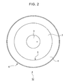
- FIG. 1 A vertical sectional view of an antenna device of the present invention is shown in Fig. 1 and a top view of the antenna device of the present invention is shown in Fig. 2.
- the shape of a metal plate (1) serving as a ground plate, a dielectric substrate (2) as a substrate, and a metal plate (3) as a microstrip patch is circular, respectively.
- the shape of the metal plate (1), the dielectric substrate (2) or the metal plate (3) may be a quasi circular.
- the metal plate (1) as a ground plate and the dielectric substrate (2) generally have the same size and the same shape, but they must not have the same size and the same shape.
- the metal plate (1) as a ground plate may be made a square form containing the dielectric substrate (2) therein.
- the metal plate (1) as a ground plate and the dielectric substrate (2) have the same size and shape.
- the radius of the metal plate (3) as a circular microstrip patch can be approximately obtained with the following formula (hereinafter, referred to as formula 1).
- F 1.841 ⁇ C/[2 ⁇ a+2(t/ ⁇ )1n2 ⁇ ⁇ ]
- F is the resonance frequency, that is, the frequency of a signal wave as a target of an antenna device of the present invention
- C is the light velocity
- a is the radius of a circular microstrip patch
- t is the thickness of the substrate
- ⁇ ⁇ is the dielectric constant of the substrate.
- a wavelength represents the wavelength ⁇ of a signal wave as an object of an antenna device (12) of the present invention.
- the diameter of the metal plate (1) as a ground plate and the dielectric substrate (2), that is, the portion represented by D in Fig. 1 is about one wavelength long.
- the metal plate is a metal having a low electric resistance, usually a relatively low-priced copper of a sufficiently low electric resistance is used. Furthermore, different metals may be used for the metal plate (1) as a ground plate and the metal plate (3) as a microstrip patch, but normally the same metal is used.
- the dielectric substrate (2) As a dielectric substrate, there are a glass epoxy resin, polyethylene resin, ceramic dielectric material, etc., but publicly known dielectric materials for the microstrip antenna in the past may be used. Furthermore, as shown in Fig. 3, the dielectric substrate (2) may be formed by using a honeycomb material (9). In this way, a broadband antenna device can be realized.
- the metal plate (1) as a ground plate and the dielectric substrate (2) are glued so as to be in agreement with each other, and the metal plate (3) as a microstrip patch is normally glued in the middle portion of the dielectric substrate (2) such that the metal plate (3) does not protrude from the dielectric substrate (2).
- the portion of the metal left after the removal functions as a microstrip patch and, since the resonance frequency is controlled by the size of the microstrip patch, the resonance frequency can be set such that the portion to be removed of the metal plate is adjusted.
- the above method is not necessarily required, and any publicly known method in the past may be appropriately used.
- a conical cup (4) which is a substantially conical conductive member having both upper and lower sides made open is formed by using a metal.
- a metal although the use of a material different from the metal plate (1) as a ground plate and the metal plate (3) as a microstrip patch is not excluded, in order to avoid the affect due to inherent impedances depending on each kind of metals when the different metals are used, normally the same materials are used. In the present embodiment, the material of copper is used.
- the lower opening portion (5) of the conical cup (4) is circular, the diameter is substantially the same as that of the dielectric substrate (2) and the metal plate (1) as a ground plate, and the opening portion (5) is made in contact with the surrounding edge portion of the dielectric substrate (2) and the metal plate (1) as a ground plate.
- the conical cup (4) is not necessarily required to be made in contact with the dielectric substrate (2), and it is enough that at least the conical cup (4) is made in contact with the metal plate (1) as a ground plate.
- a welding method by soldering may be used. In this way, while being grounded to the metal plate (1) as a ground plate, the conical cup (4) is vertically erected around the metal plate (3) as a microstrip patch.
- the gradient of a side wall portion (7) as the ringshaped body of the conical cup (4) is normally substantially constant.
- the upper opening portion (6) opposite to the dielectric substrate (2) of the conical cup (4) is circular, and the diameter, that is, the portion represented by DL in Fig. 1 is about 3/2 a wavelength.
- the height of the conical cup (4), that is, the portion represented by H in Fig. 1 is about 1/3 a wavelength.
- a parasitic microstrip patch (10) and a substrate (11) for the parasitic microstrip patch may be provided in the front of the radiation surface of the microstrip patch.
- the dielectric substrate (2) is formed by using a honeycomb material (9) and, in addition to that, a parasitic microstrip patch (10) and a substrate (11) for the parasitic microstrip patch may be provided in the front of the radiation surface of the microstrip patch.
- a publicly known method in the past may be used.
- a pin-type feeder in which a feeding connector (8) is provided in the metal plate (1) as a ground plate is provided is used.
- the frequency of a signal wave as an object of the antenna device (12) is set to be 2.5 GHz, and a PTFE dielectric material having a dielectric constant of 2.17 and a thickness of 1.524 mm is used.
- the wavelength of a signal wave as an object for transmission and reception of the antenna device becomes 120 mm. Furthermore, by using the above formula 1, the radius of the microstrip patch was calculated and set to be 46 mm (23/60 a wavelength). A copper material was used for the microstrip patch, ground plate, and conical cup. The thickness of the conical cup was set to be 0.2 mm.
- a table showing the change of gain to the height of a cylinder cup when the cylinder cup of a substantially cylindrical conductive member is provided around the microstrip antenna is shown. From the computation values and measurement values in Fig. 5, it was understood that high gains can be obtained in the range where the height of the cylinder cup is from about 40 mm (about 1/3 a wavelength) to about 60 mm (1/2 a wavelength). Accordingly, it is found that it is desirable that, when a conical cup is provided, in order to obtain a high gain, the height of the conical cup is set to be from about 40 mm (1/3 a wavelength) to about 60 mm) 1/2 a wavelength) in the same way as in the case where the cylinder cup is provided.
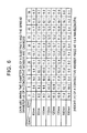
- the height of the conical cup is fixed at 40 mm (1/3 a wavelength) and, when the diameter and spread diameter of the substrate (as an indicator showing the degree of expansion of the upper opening portion of the conical cup, a half of the difference between the diameter of the ground plate and the dielectric substrate and the diameter of the upper opening portion, that is, the portion represented by d in Fig. 1 is defined as a spread diameter of the substrate) are changed, the change of gain (computation value) is shown in Fig. 6. Furthermore, in the same way, the height of the conical cup is fixed at 40 mm (1/3 a wavelength) and, when the diameter and spread diameter of the substrate is changed, the change of a beam width (computation value) is shown in Fig. 7.
- the diameter of the substrate is changed from 80 mm (2/3 a wavelength) to 150 mm (5/4 a wavelength) and the spread diameter is changed from zero mm (zero a wavelength) to 50 mm (5/12 a wavelength).
- the changes are not limited to those and shown only as examples. From these figures, it is understood that the improvement of gain and/or the attainment of a narrow beam width is practicable such that a substantially conical conductive material is provided around the microstrip patch. Then, an antenna device having a gain and beam width for desired purposes can be constituted such that the diameter of the substrate and the spread diameter are properly combined. Moreover, even if various wavelength areas are used without limiting to the present embodiment, the same effect can be obtained.
- the present inventor et al. practically took measurement of the gain and beam width of a part of the objects of the above numerical computation, and the result of the measurement is shown.
- the height of the conical cup is set at 40 mm (1/3 a wavelength) and the diameter of the dielectric substrate is set at 120 mm (one wave length)
- the change of gain (measurement value) when the spread diameter is changed is shown in Fig. 8.
- the height of the conical cup is set at 40 mm (1/3 a wavelength) and the diameter of the dielectric substrate is set at 120 mm (one wave length)
- the change of a beam width (measurement value) in the H plane(the plane containing the magnetic-field vector of an electromagnetic wave) and the E plane (the plane containing the electric-field vector of an electromagnetic wave) of the antenna pattern is shown in Fig. 9.
- a beam width measured value
- the computation values and the measurement values a similarity can be seen between the tendencies of change of the computation values and the measurement values for the gain and the beam width when the spread diameter is changed. Therefore, not only in the numerical computation, but also practically, the improvement of gain and/or the attainment of a narrow beam width was confirmed such that a substantially conical conductive member is provided around the microstrip patch.
- an antenna device having a gain and beam width for desired purposes can be constituted such that the conical cup (4) is freely changed.
- an antenna device having a gain and beam width for desired purposes can be constituted such that a conductive member of a combination of an appropriate diameter of a substrate and a spread diameter is provided around a microstrip patch. Furthermore, an antenna device having a high gain and narrow beam width which are consistent with each other can be constituted, although dependent on a combination of the diameter of a substrate and the spread diameter. Moreover, an antenna device of the present invention is also characterized by being small and light in the same way as a microstrip antenna is.
- the antenna device can be used as a primary radiator of a reflector antenna. Furthermore, it is also able to consider applications of a mobile station antenna, portable station antenna, satellite-mounted antenna, or a primary radiator for these, and, as a result, an antenna device of the present invention can be utilized in a wide range of fields in the industry.
Landscapes
- Waveguide Aerials (AREA)
- Control And Other Processes For Unpacking Of Materials (AREA)
- Burglar Alarm Systems (AREA)
- Radar Systems Or Details Thereof (AREA)
- Details Of Aerials (AREA)
- Aerials With Secondary Devices (AREA)
Abstract
Description
- 1
- metal plate as a ground plate
- 2
- dielectric substrate as a substrate
- 3
- metal plate as a microstrip patch
- 4
- conical cup as a conductive member
- 5
- lower opening portion
- 6
- upper opening portion
- 7
- side wall portion of a conductive member
- 8
- feed connector
- 9
- honeycomb material
- 10
- parasitic microstrip patch
- 11
- substrate for a parasitic microstrip patch
- 12
- antenna device of the present invention
Claims (7)
- An antenna device comprising:wherein the lower opening portion of the conductive member is grounded to a ground plate provided on the lower side of the substrate, anda substantially circular substrate;a substantially circular microstrip patch provided on the upper surface of the substrate; anda substantially cylindrical conductive member having upper and lower opening portions erected in a substantially vertical direction around the microstrip patch,
wherein the diameter of the upper opening portion of the conductive member is larger than the diameter of the lower opening portion of the conductive member. - An antenna device as claimed in claim 1, wherein, to a wavelength of a signal wave serving as an object of an antenna device, the height of the conductive member is from about 1/3 a wavelength to about 1/2 a wavelength.
- An antenna device as claimed in claim 1, wherein, to a wavelength of a signal wave serving as an object of an antenna device, the height of the conductive member is about 1/3 a wavelength, the diameter of the substrate is from about 3/4 a wavelength to about 5/4 a wavelength, and the diameter of the upper opening portion of the conductive member is from about 13/12 a wavelength to about 11/6 a wavelength.
- An antenna device as claimed in claim 1, wherein, to a wavelength of a signal wave serving as an object of an antenna device, the height of the conductive member is about 1/3 a wavelength, the diameter of the substrate is about a wavelength, and the diameter of the upper opening portion of the conductive member is about 3/2 a wavelength.
- An antenna device as claimed in any one of claims 1 to 4, wherein the substrate is made up of a honeycomb material.
- An antenna device as claimed in any one of claims 1 to 5, wherein a parasitic microstrip patch is provided in the front of the radiation surface of the microstrip patch.
- An antenna device as claimed in any one of claims 1 to 6, wherein the conductive member can be freely changed.
Applications Claiming Priority (1)
| Application Number | Priority Date | Filing Date | Title |
|---|---|---|---|
| PCT/JP2002/011131 WO2004038862A1 (en) | 2002-10-25 | 2002-10-25 | Antenna device |
Publications (3)
| Publication Number | Publication Date |
|---|---|
| EP1555721A1 true EP1555721A1 (en) | 2005-07-20 |
| EP1555721A4 EP1555721A4 (en) | 2006-01-25 |
| EP1555721B1 EP1555721B1 (en) | 2007-09-05 |
Family
ID=32170790
Family Applications (1)
| Application Number | Title | Priority Date | Filing Date |
|---|---|---|---|
| EP02808056A Expired - Lifetime EP1555721B1 (en) | 2002-10-25 | 2002-10-25 | Antenna device |
Country Status (7)
| Country | Link |
|---|---|
| US (1) | US7187328B2 (en) |
| EP (1) | EP1555721B1 (en) |
| JP (1) | JPWO2004038862A1 (en) |
| CN (1) | CN100490248C (en) |
| AT (1) | ATE372593T1 (en) |
| DE (1) | DE60222308D1 (en) |
| WO (1) | WO2004038862A1 (en) |
Cited By (5)
| Publication number | Priority date | Publication date | Assignee | Title |
|---|---|---|---|---|
| WO2008124356A1 (en) * | 2007-04-04 | 2008-10-16 | Symbol Technologies, Inc. | Rfid antenna cupped reflector |
| ITRM20100511A1 (en) * | 2010-10-01 | 2012-04-02 | Clu Tech Srl | HYBRID PRINTED ANTENNA WITH MULTIPLE RADIANT ELEMENTS |
| ITRM20100512A1 (en) * | 2010-10-01 | 2012-04-02 | Clu Tech Srl | HYBRID OPENING ANTENNA WITH REFLECTOR |
| WO2014111505A1 (en) * | 2013-01-18 | 2014-07-24 | Astrium Sas | Antenna having a miniaturised waveguide |
| US9761929B1 (en) * | 2016-04-26 | 2017-09-12 | Dennis D. McPhearson | Multi bandwidth cellular antenna |
Families Citing this family (37)
| Publication number | Priority date | Publication date | Assignee | Title |
|---|---|---|---|---|
| KR100603604B1 (en) * | 2004-12-16 | 2006-07-24 | 한국전자통신연구원 | Flat-top element pattern forming apparatus using circularly polarized microstrip patch |
| KR100731278B1 (en) * | 2005-01-31 | 2007-06-25 | 주식회사 와이어리스데이터커뮤니케이션 | Antenna assembly |
| US20070268188A1 (en) * | 2006-04-26 | 2007-11-22 | Spotwave Wireless Canada, Inc. | Ground plane patch antenna |
| US20080081555A1 (en) * | 2006-10-03 | 2008-04-03 | Wireless Data Communication Co., Ltd | Unified communication repeater |
| US20080129631A1 (en) * | 2006-12-05 | 2008-06-05 | Chih-Ming Chen | Broadband circularly polarization antenna device |
| US8212734B1 (en) * | 2007-11-15 | 2012-07-03 | Lockheed Martin Corporation | Hybrid reflector with radiating subreflector |
| CZ305165B6 (en) * | 2008-06-17 | 2015-05-27 | Petr Drexler | Sensor to measure extremely short, isolated electromagnetic pulses |
| US7936306B2 (en) * | 2008-09-23 | 2011-05-03 | Kathrein-Werke Kg | Multilayer antenna arrangement |
| JP4987840B2 (en) * | 2008-12-02 | 2012-07-25 | 株式会社東芝 | ANTENNA DEVICE AND WIRELESS COMMUNICATION SYSTEM |
| DE102009005045A1 (en) * | 2009-01-13 | 2010-07-15 | Wilhelm Sihn Jr. Gmbh & Co. Kg | patch antenna |
| KR101013388B1 (en) * | 2009-02-27 | 2011-02-14 | 주식회사 모비텍 | MIO antenna with parasitic elements |
| US8766854B2 (en) * | 2010-01-07 | 2014-07-01 | National Taiwan University | Bottom feed cavity aperture antenna |
| US9930592B2 (en) | 2013-02-19 | 2018-03-27 | Mimosa Networks, Inc. | Systems and methods for directing mobile device connectivity |
| US9179336B2 (en) | 2013-02-19 | 2015-11-03 | Mimosa Networks, Inc. | WiFi management interface for microwave radio and reset to factory defaults |
| WO2014138292A1 (en) | 2013-03-06 | 2014-09-12 | Mimosa Networks, Inc. | Enclosure for radio, parabolic dish antenna, and side lobe shields |
| US9130305B2 (en) | 2013-03-06 | 2015-09-08 | Mimosa Networks, Inc. | Waterproof apparatus for cables and cable interfaces |
| US10742275B2 (en) | 2013-03-07 | 2020-08-11 | Mimosa Networks, Inc. | Quad-sector antenna using circular polarization |
| US9191081B2 (en) | 2013-03-08 | 2015-11-17 | Mimosa Networks, Inc. | System and method for dual-band backhaul radio |
| US9295103B2 (en) | 2013-05-30 | 2016-03-22 | Mimosa Networks, Inc. | Wireless access points providing hybrid 802.11 and scheduled priority access communications |
| US10938110B2 (en) | 2013-06-28 | 2021-03-02 | Mimosa Networks, Inc. | Ellipticity reduction in circularly polarized array antennas |
| US9001689B1 (en) | 2014-01-24 | 2015-04-07 | Mimosa Networks, Inc. | Channel optimization in half duplex communications systems |
| US9998246B2 (en) | 2014-03-13 | 2018-06-12 | Mimosa Networks, Inc. | Simultaneous transmission on shared channel |
| US10958332B2 (en) | 2014-09-08 | 2021-03-23 | Mimosa Networks, Inc. | Wi-Fi hotspot repeater |
| KR101709077B1 (en) * | 2015-11-20 | 2017-02-22 | 현대자동차주식회사 | Antenna apparatus, manufacture method of antenna apparatus, vehicle having the same |
| US10749263B2 (en) * | 2016-01-11 | 2020-08-18 | Mimosa Networks, Inc. | Printed circuit board mounted antenna and waveguide interface |
| US11251539B2 (en) | 2016-07-29 | 2022-02-15 | Airspan Ip Holdco Llc | Multi-band access point antenna array |
| CN106654559A (en) * | 2016-12-23 | 2017-05-10 | 电子科技大学 | High-gain microstrip patch antenna combined module antenna |
| KR102402411B1 (en) | 2017-06-28 | 2022-05-27 | 삼성전자주식회사 | Antenna device and electronic device comprising antenna |
| WO2019087733A1 (en) * | 2017-11-06 | 2019-05-09 | 株式会社村田製作所 | Antenna substrate and antenna module |
| US10511074B2 (en) | 2018-01-05 | 2019-12-17 | Mimosa Networks, Inc. | Higher signal isolation solutions for printed circuit board mounted antenna and waveguide interface |
| WO2019168800A1 (en) | 2018-03-02 | 2019-09-06 | Mimosa Networks, Inc. | Omni-directional orthogonally-polarized antenna system for mimo applications |
| US11101565B2 (en) * | 2018-04-26 | 2021-08-24 | Neptune Technology Group Inc. | Low-profile antenna |
| US11289821B2 (en) | 2018-09-11 | 2022-03-29 | Air Span Ip Holdco Llc | Sector antenna systems and methods for providing high gain and high side-lobe rejection |
| US11233336B2 (en) * | 2019-02-08 | 2022-01-25 | Samsung Electro-Mechanics Co., Ltd. | Chip antenna and chip antenna module including the same |
| KR102608773B1 (en) * | 2019-02-14 | 2023-12-04 | 삼성전자주식회사 | Antenna module and electronic device including the same |
| JP7580037B2 (en) * | 2019-10-02 | 2024-11-11 | パナソニックIpマネジメント株式会社 | Antenna device and vehicle |
| CN113948859A (en) * | 2021-11-01 | 2022-01-18 | 深圳市华信天线技术有限公司 | Microstrip antenna |
Family Cites Families (17)
| Publication number | Priority date | Publication date | Assignee | Title |
|---|---|---|---|---|
| US4660048A (en) * | 1984-12-18 | 1987-04-21 | Texas Instruments Incorporated | Microstrip patch antenna system |
| JPS62118613A (en) * | 1985-11-19 | 1987-05-30 | Nippon Telegr & Teleph Corp <Ntt> | Circularly polarized wave horn antenna |
| FR2592232B1 (en) * | 1985-12-20 | 1988-02-12 | Radiotechnique Compelec | MICROWAVE PLANE ANTENNA WITH SUSPENDED SUBSTRATE LINES ARRAY AND METHOD FOR MANUFACTURING THE SAME. |
| JPH05206721A (en) * | 1992-01-28 | 1993-08-13 | Toshiba Corp | Antenna device |
| JPH07297625A (en) * | 1994-04-27 | 1995-11-10 | Sony Corp | Microstrip antenna |
| JPH07326921A (en) * | 1994-05-31 | 1995-12-12 | Sony Corp | Microstrip array antenna |
| JP2957463B2 (en) * | 1996-03-11 | 1999-10-04 | 日本電気株式会社 | Patch antenna and method of manufacturing the same |
| US5889498A (en) | 1996-10-28 | 1999-03-30 | California Amplifier Company | End-fire array antennas with divergent reflector |
| JPH10224141A (en) * | 1997-02-10 | 1998-08-21 | Toshiba Corp | Monolithic antenna |
| JP3026171B2 (en) * | 1997-02-27 | 2000-03-27 | 郵政省通信総合研究所長 | Antenna device |
| US6593887B2 (en) * | 1999-01-25 | 2003-07-15 | City University Of Hong Kong | Wideband patch antenna with L-shaped probe |
| JP2001168632A (en) * | 1999-12-13 | 2001-06-22 | Nippon Antenna Co Ltd | Horn antenna and primary radiator |
| EP1158604B1 (en) * | 2000-05-26 | 2006-07-19 | Matsushita Electric Industrial Co., Ltd. | Antenna, antenna device, and radio equipment |
| US6538618B2 (en) * | 2000-10-13 | 2003-03-25 | Matsushita Electric Industrial Co., Ltd. | Antenna |
| US6597316B2 (en) * | 2001-09-17 | 2003-07-22 | The Mitre Corporation | Spatial null steering microstrip antenna array |
| US6891513B2 (en) * | 2001-11-26 | 2005-05-10 | Vega Greishaber, Kg | Antenna system for a level measurement apparatus |
| CA2422345A1 (en) * | 2002-03-27 | 2003-09-27 | Her Majesty The Queen In Right Of Canada As Represented By The Minister Of Her Majesty's Canadian Government | Non-planar ringed antenna system |
-
2002
- 2002-10-25 US US10/532,298 patent/US7187328B2/en not_active Expired - Fee Related
- 2002-10-25 DE DE60222308T patent/DE60222308D1/en not_active Expired - Lifetime
- 2002-10-25 CN CNB028297962A patent/CN100490248C/en not_active Expired - Fee Related
- 2002-10-25 AT AT02808056T patent/ATE372593T1/en not_active IP Right Cessation
- 2002-10-25 JP JP2004546382A patent/JPWO2004038862A1/en active Pending
- 2002-10-25 EP EP02808056A patent/EP1555721B1/en not_active Expired - Lifetime
- 2002-10-25 WO PCT/JP2002/011131 patent/WO2004038862A1/en not_active Ceased
Cited By (6)
| Publication number | Priority date | Publication date | Assignee | Title |
|---|---|---|---|---|
| WO2008124356A1 (en) * | 2007-04-04 | 2008-10-16 | Symbol Technologies, Inc. | Rfid antenna cupped reflector |
| ITRM20100511A1 (en) * | 2010-10-01 | 2012-04-02 | Clu Tech Srl | HYBRID PRINTED ANTENNA WITH MULTIPLE RADIANT ELEMENTS |
| ITRM20100512A1 (en) * | 2010-10-01 | 2012-04-02 | Clu Tech Srl | HYBRID OPENING ANTENNA WITH REFLECTOR |
| WO2014111505A1 (en) * | 2013-01-18 | 2014-07-24 | Astrium Sas | Antenna having a miniaturised waveguide |
| FR3001342A1 (en) * | 2013-01-18 | 2014-07-25 | Astrium Sas | MINIATURIZED ANTENNA |
| US9761929B1 (en) * | 2016-04-26 | 2017-09-12 | Dennis D. McPhearson | Multi bandwidth cellular antenna |
Also Published As
| Publication number | Publication date |
|---|---|
| EP1555721A4 (en) | 2006-01-25 |
| WO2004038862A1 (en) | 2004-05-06 |
| EP1555721B1 (en) | 2007-09-05 |
| US7187328B2 (en) | 2007-03-06 |
| CN100490248C (en) | 2009-05-20 |
| ATE372593T1 (en) | 2007-09-15 |
| CN1689192A (en) | 2005-10-26 |
| DE60222308D1 (en) | 2007-10-18 |
| JPWO2004038862A1 (en) | 2006-02-23 |
| US20060139209A1 (en) | 2006-06-29 |
Similar Documents
| Publication | Publication Date | Title |
|---|---|---|
| US7187328B2 (en) | Antenna device | |
| US10971824B2 (en) | Antenna element | |
| EP3168927B1 (en) | Ultra compact ultra broad band dual polarized base station antenna | |
| KR101059047B1 (en) | Metamaterial Omni-directional Circularly Polarized Antenna | |
| US11133601B2 (en) | Fractal-rectangular reactive impedance surface for antenna miniaturization | |
| US20150303576A1 (en) | Miniaturized Patch Antenna | |
| EP2533362B1 (en) | Microstrip antenna and radar module | |
| KR101709763B1 (en) | Hardened wave-guide antenna | |
| EP1684381B1 (en) | Patch antenna with comb substrate | |
| CN105990681B (en) | Antenna and airborne communication equipment | |
| US12062864B2 (en) | High gain and fan beam antenna structures | |
| KR101868184B1 (en) | Dual antenna structure having circular polarisation characteristics | |
| WO2016069014A1 (en) | Dielectric resonator antenna | |
| US20050275593A1 (en) | Method and device for loading planar antennas | |
| CN103247849A (en) | Antenna device | |
| WO2021197400A1 (en) | A patch antenna | |
| CN211045725U (en) | Circularly polarized antenna | |
| CN112271438A (en) | Slot-fed circularly polarized omnidirectional dielectric resonator antenna | |
| US6727858B2 (en) | Circularly polarized wave antenna suitable for miniaturization | |
| US11450967B2 (en) | Slot antenna | |
| CN220821922U (en) | Circularly polarized wide beam microstrip antenna with stable phase center | |
| JP2023503294A (en) | Electromagnetic bandgap structure | |
| CN112542688B (en) | Microstrip antenna and terminal equipment | |
| EP0402005A2 (en) | Flush mount antenna | |
| JP2015154368A (en) | Patch antenna |
Legal Events
| Date | Code | Title | Description |
|---|---|---|---|
| PUAI | Public reference made under article 153(3) epc to a published international application that has entered the european phase |
Free format text: ORIGINAL CODE: 0009012 |
|
| 17P | Request for examination filed |
Effective date: 20050513 |
|
| AK | Designated contracting states |
Kind code of ref document: A1 Designated state(s): AT BE BG CH CY CZ DE DK EE ES FI FR GB GR IE IT LI LU MC NL PT SE SK TR |
|
| A4 | Supplementary search report drawn up and despatched |
Effective date: 20051213 |
|
| RIC1 | Information provided on ipc code assigned before grant |
Ipc: H01Q 13/02 19680901AFI20040511BHEP Ipc: H01Q 19/22 19680901ALI20051207BHEP Ipc: H01Q 13/08 19680901ALI20051207BHEP |
|
| RIN1 | Information on inventor provided before grant (corrected) |
Inventor name: PARK, BYUNG S. Inventor name: JANG, JAE H. Inventor name: TANAKA, MASATO, Inventor name: KIM, YUNG SIK,KOREA UNIVERSITY |
|
| RIN1 | Information on inventor provided before grant (corrected) |
Inventor name: PARK, BYUNG S. Inventor name: JANG, JAE H.C/O INTELLECTUAL PROP. MAN. GROUP Inventor name: TANAKA, MASATO, Inventor name: KIM, YUNG SIK,KOREA UNIVERSITY |
|
| RIN1 | Information on inventor provided before grant (corrected) |
Inventor name: JANG, JAE H.INTELL. PROP. MANAGEMENT. GROUP. Inventor name: TANAKA, MASATO, Inventor name: KIM, YUNG SIK,KOREA UNIVERSITY Inventor name: PARK, BYUNG S. |
|
| GRAP | Despatch of communication of intention to grant a patent |
Free format text: ORIGINAL CODE: EPIDOSNIGR1 |
|
| RAP1 | Party data changed (applicant data changed or rights of an application transferred) |
Owner name: NATIONAL INSTITUTE OF INFORMATION AND C |
|
| RIN1 | Information on inventor provided before grant (corrected) |
Inventor name: TANAKA, MASATO, Inventor name: PARK, BYUNG S. Inventor name: JANG, JAE H.NATIONAL INSTITUTE OF INFORMATION AND Inventor name: KIM, YUNG SIK,KOREA UNIVERSITY |
|
| GRAS | Grant fee paid |
Free format text: ORIGINAL CODE: EPIDOSNIGR3 |
|
| GRAA | (expected) grant |
Free format text: ORIGINAL CODE: 0009210 |
|
| RIN1 | Information on inventor provided before grant (corrected) |
Inventor name: TANAKA, MASATO, Inventor name: PARK, BYUNGSUN Inventor name: JANG, JAE H.NATIONAL INSTITUTE OF INFORMATION AND Inventor name: KIM, YUNG SIK,KOREA UNIVERSITY |
|
| AK | Designated contracting states |
Kind code of ref document: B1 Designated state(s): AT BE BG CH CY CZ DE DK EE ES FI FR GB GR IE IT LI LU MC NL PT SE SK TR |
|
| REG | Reference to a national code |
Ref country code: GB Ref legal event code: FG4D |
|
| RIN1 | Information on inventor provided before grant (corrected) |
Inventor name: TANAKA, MASATONATIONAL INSTITUTE OF INFORMATION AN Inventor name: JANG, JAE H.NATIONAL INSTITUTE OF INFORMATION AND Inventor name: KIM, YUNG SIK,KOREA UNIVERSITY Inventor name: PARK, BYUNGSUN |
|
| REG | Reference to a national code |
Ref country code: CH Ref legal event code: EP |
|
| REF | Corresponds to: |
Ref document number: 60222308 Country of ref document: DE Date of ref document: 20071018 Kind code of ref document: P |
|
| REG | Reference to a national code |
Ref country code: IE Ref legal event code: FG4D |
|
| PG25 | Lapsed in a contracting state [announced via postgrant information from national office to epo] |
Ref country code: FI Free format text: LAPSE BECAUSE OF FAILURE TO SUBMIT A TRANSLATION OF THE DESCRIPTION OR TO PAY THE FEE WITHIN THE PRESCRIBED TIME-LIMIT Effective date: 20070905 Ref country code: ES Free format text: LAPSE BECAUSE OF FAILURE TO SUBMIT A TRANSLATION OF THE DESCRIPTION OR TO PAY THE FEE WITHIN THE PRESCRIBED TIME-LIMIT Effective date: 20071216 |
|
| PG25 | Lapsed in a contracting state [announced via postgrant information from national office to epo] |
Ref country code: CH Free format text: LAPSE BECAUSE OF FAILURE TO SUBMIT A TRANSLATION OF THE DESCRIPTION OR TO PAY THE FEE WITHIN THE PRESCRIBED TIME-LIMIT Effective date: 20070905 Ref country code: AT Free format text: LAPSE BECAUSE OF FAILURE TO SUBMIT A TRANSLATION OF THE DESCRIPTION OR TO PAY THE FEE WITHIN THE PRESCRIBED TIME-LIMIT Effective date: 20070905 Ref country code: LI Free format text: LAPSE BECAUSE OF FAILURE TO SUBMIT A TRANSLATION OF THE DESCRIPTION OR TO PAY THE FEE WITHIN THE PRESCRIBED TIME-LIMIT Effective date: 20070905 |
|
| NLV1 | Nl: lapsed or annulled due to failure to fulfill the requirements of art. 29p and 29m of the patents act | ||
| PG25 | Lapsed in a contracting state [announced via postgrant information from national office to epo] |
Ref country code: BE Free format text: LAPSE BECAUSE OF FAILURE TO SUBMIT A TRANSLATION OF THE DESCRIPTION OR TO PAY THE FEE WITHIN THE PRESCRIBED TIME-LIMIT Effective date: 20070905 |
|
| REG | Reference to a national code |
Ref country code: CH Ref legal event code: PL |
|
| PG25 | Lapsed in a contracting state [announced via postgrant information from national office to epo] |
Ref country code: DE Free format text: LAPSE BECAUSE OF FAILURE TO SUBMIT A TRANSLATION OF THE DESCRIPTION OR TO PAY THE FEE WITHIN THE PRESCRIBED TIME-LIMIT Effective date: 20071206 Ref country code: NL Free format text: LAPSE BECAUSE OF FAILURE TO SUBMIT A TRANSLATION OF THE DESCRIPTION OR TO PAY THE FEE WITHIN THE PRESCRIBED TIME-LIMIT Effective date: 20070905 Ref country code: GR Free format text: LAPSE BECAUSE OF FAILURE TO SUBMIT A TRANSLATION OF THE DESCRIPTION OR TO PAY THE FEE WITHIN THE PRESCRIBED TIME-LIMIT Effective date: 20071206 |
|
| EN | Fr: translation not filed | ||
| PG25 | Lapsed in a contracting state [announced via postgrant information from national office to epo] |
Ref country code: SK Free format text: LAPSE BECAUSE OF FAILURE TO SUBMIT A TRANSLATION OF THE DESCRIPTION OR TO PAY THE FEE WITHIN THE PRESCRIBED TIME-LIMIT Effective date: 20070905 Ref country code: MC Free format text: LAPSE BECAUSE OF NON-PAYMENT OF DUE FEES Effective date: 20071031 Ref country code: CZ Free format text: LAPSE BECAUSE OF FAILURE TO SUBMIT A TRANSLATION OF THE DESCRIPTION OR TO PAY THE FEE WITHIN THE PRESCRIBED TIME-LIMIT Effective date: 20070905 Ref country code: PT Free format text: LAPSE BECAUSE OF FAILURE TO SUBMIT A TRANSLATION OF THE DESCRIPTION OR TO PAY THE FEE WITHIN THE PRESCRIBED TIME-LIMIT Effective date: 20080206 |
|
| PG25 | Lapsed in a contracting state [announced via postgrant information from national office to epo] |
Ref country code: SE Free format text: LAPSE BECAUSE OF FAILURE TO SUBMIT A TRANSLATION OF THE DESCRIPTION OR TO PAY THE FEE WITHIN THE PRESCRIBED TIME-LIMIT Effective date: 20071205 |
|
| PLBE | No opposition filed within time limit |
Free format text: ORIGINAL CODE: 0009261 |
|
| STAA | Information on the status of an ep patent application or granted ep patent |
Free format text: STATUS: NO OPPOSITION FILED WITHIN TIME LIMIT |
|
| PG25 | Lapsed in a contracting state [announced via postgrant information from national office to epo] |
Ref country code: DK Free format text: LAPSE BECAUSE OF FAILURE TO SUBMIT A TRANSLATION OF THE DESCRIPTION OR TO PAY THE FEE WITHIN THE PRESCRIBED TIME-LIMIT Effective date: 20070905 |
|
| 26N | No opposition filed |
Effective date: 20080606 |
|
| PG25 | Lapsed in a contracting state [announced via postgrant information from national office to epo] |
Ref country code: FR Free format text: LAPSE BECAUSE OF FAILURE TO SUBMIT A TRANSLATION OF THE DESCRIPTION OR TO PAY THE FEE WITHIN THE PRESCRIBED TIME-LIMIT Effective date: 20080502 |
|
| PG25 | Lapsed in a contracting state [announced via postgrant information from national office to epo] |
Ref country code: IE Free format text: LAPSE BECAUSE OF NON-PAYMENT OF DUE FEES Effective date: 20071025 |
|
| PG25 | Lapsed in a contracting state [announced via postgrant information from national office to epo] |
Ref country code: EE Free format text: LAPSE BECAUSE OF FAILURE TO SUBMIT A TRANSLATION OF THE DESCRIPTION OR TO PAY THE FEE WITHIN THE PRESCRIBED TIME-LIMIT Effective date: 20070905 |
|
| PG25 | Lapsed in a contracting state [announced via postgrant information from national office to epo] |
Ref country code: CY Free format text: LAPSE BECAUSE OF FAILURE TO SUBMIT A TRANSLATION OF THE DESCRIPTION OR TO PAY THE FEE WITHIN THE PRESCRIBED TIME-LIMIT Effective date: 20070905 |
|
| PG25 | Lapsed in a contracting state [announced via postgrant information from national office to epo] |
Ref country code: BG Free format text: LAPSE BECAUSE OF FAILURE TO SUBMIT A TRANSLATION OF THE DESCRIPTION OR TO PAY THE FEE WITHIN THE PRESCRIBED TIME-LIMIT Effective date: 20071205 Ref country code: LU Free format text: LAPSE BECAUSE OF NON-PAYMENT OF DUE FEES Effective date: 20071025 |
|
| PG25 | Lapsed in a contracting state [announced via postgrant information from national office to epo] |
Ref country code: TR Free format text: LAPSE BECAUSE OF FAILURE TO SUBMIT A TRANSLATION OF THE DESCRIPTION OR TO PAY THE FEE WITHIN THE PRESCRIBED TIME-LIMIT Effective date: 20070905 |
|
| PG25 | Lapsed in a contracting state [announced via postgrant information from national office to epo] |
Ref country code: IT Free format text: LAPSE BECAUSE OF NON-PAYMENT OF DUE FEES Effective date: 20071031 |
|
| PGFP | Annual fee paid to national office [announced via postgrant information from national office to epo] |
Ref country code: GB Payment date: 20101020 Year of fee payment: 9 |
|
| GBPC | Gb: european patent ceased through non-payment of renewal fee |
Effective date: 20111025 |
|
| PG25 | Lapsed in a contracting state [announced via postgrant information from national office to epo] |
Ref country code: GB Free format text: LAPSE BECAUSE OF NON-PAYMENT OF DUE FEES Effective date: 20111025 |