EP1553446A1 - Pattern size correcting device and pattern size correcting method - Google Patents
Pattern size correcting device and pattern size correcting method Download PDFInfo
- Publication number
- EP1553446A1 EP1553446A1 EP03766611A EP03766611A EP1553446A1 EP 1553446 A1 EP1553446 A1 EP 1553446A1 EP 03766611 A EP03766611 A EP 03766611A EP 03766611 A EP03766611 A EP 03766611A EP 1553446 A1 EP1553446 A1 EP 1553446A1
- Authority
- EP
- European Patent Office
- Prior art keywords
- pattern
- area ratio
- open area
- size
- correcting
- Prior art date
- Legal status (The legal status is an assumption and is not a legal conclusion. Google has not performed a legal analysis and makes no representation as to the accuracy of the status listed.)
- Withdrawn
Links
Images




Classifications
-
- G—PHYSICS
- G03—PHOTOGRAPHY; CINEMATOGRAPHY; ANALOGOUS TECHNIQUES USING WAVES OTHER THAN OPTICAL WAVES; ELECTROGRAPHY; HOLOGRAPHY
- G03F—PHOTOMECHANICAL PRODUCTION OF TEXTURED OR PATTERNED SURFACES, e.g. FOR PRINTING, FOR PROCESSING OF SEMICONDUCTOR DEVICES; MATERIALS THEREFOR; ORIGINALS THEREFOR; APPARATUS SPECIALLY ADAPTED THEREFOR
- G03F1/00—Originals for photomechanical production of textured or patterned surfaces, e.g., masks, photo-masks, reticles; Mask blanks or pellicles therefor; Containers specially adapted therefor; Preparation thereof
- G03F1/36—Masks having proximity correction features; Preparation thereof, e.g. optical proximity correction [OPC] design processes
-
- G—PHYSICS
- G03—PHOTOGRAPHY; CINEMATOGRAPHY; ANALOGOUS TECHNIQUES USING WAVES OTHER THAN OPTICAL WAVES; ELECTROGRAPHY; HOLOGRAPHY
- G03F—PHOTOMECHANICAL PRODUCTION OF TEXTURED OR PATTERNED SURFACES, e.g. FOR PRINTING, FOR PROCESSING OF SEMICONDUCTOR DEVICES; MATERIALS THEREFOR; ORIGINALS THEREFOR; APPARATUS SPECIALLY ADAPTED THEREFOR
- G03F1/00—Originals for photomechanical production of textured or patterned surfaces, e.g., masks, photo-masks, reticles; Mask blanks or pellicles therefor; Containers specially adapted therefor; Preparation thereof
- G03F1/38—Masks having auxiliary features, e.g. special coatings or marks for alignment or testing; Preparation thereof
- G03F1/44—Testing or measuring features, e.g. grid patterns, focus monitors, sawtooth scales or notched scales
-
- G—PHYSICS
- G03—PHOTOGRAPHY; CINEMATOGRAPHY; ANALOGOUS TECHNIQUES USING WAVES OTHER THAN OPTICAL WAVES; ELECTROGRAPHY; HOLOGRAPHY
- G03F—PHOTOMECHANICAL PRODUCTION OF TEXTURED OR PATTERNED SURFACES, e.g. FOR PRINTING, FOR PROCESSING OF SEMICONDUCTOR DEVICES; MATERIALS THEREFOR; ORIGINALS THEREFOR; APPARATUS SPECIALLY ADAPTED THEREFOR
- G03F7/00—Photomechanical, e.g. photolithographic, production of textured or patterned surfaces, e.g. printing surfaces; Materials therefor, e.g. comprising photoresists; Apparatus specially adapted therefor
- G03F7/70—Microphotolithographic exposure; Apparatus therefor
- G03F7/70425—Imaging strategies, e.g. for increasing throughput or resolution, printing product fields larger than the image field or compensating lithography- or non-lithography errors, e.g. proximity correction, mix-and-match, stitching or double patterning
- G03F7/70433—Layout for increasing efficiency or for compensating imaging errors, e.g. layout of exposure fields for reducing focus errors; Use of mask features for increasing efficiency or for compensating imaging errors
- G03F7/70441—Optical proximity correction [OPC]
Definitions
- the present invention relates to a pattern size correcting device and a pattern size correcting method for correcting the size of a device pattern formed in a lithography process which is one of the manufacturing processes of a semiconductor device, and is suitably applied to various kinds of devices, for example, semiconductor chips such as IC and LSI, display elements such as a liquid crystal panel, detecting elements such as a magnetic head, imaging elements such as CCD, and so on.
- semiconductor chips such as IC and LSI
- display elements such as a liquid crystal panel
- detecting elements such as a magnetic head
- imaging elements such as CCD, and so on.
- the photolithography is a method of forming a desired pattern on a reticle being a photomask and transferring the pattern on a sample substrate via a reduction optical system.
- Photosensitive resin called a resist is formed on the sample substrate, and making use of a difference, between an exposed portion and an unexposed portion, in dissolving rate in a developing solution, a latent image of the transferred pattern is developed to form a pattern, and then etching follows, so that a material can be processed as desired.
- OPC Optical Proximity Correction
- a correction amount of a transferred image of the pattern is calculated based on the influence of an optical proximity effect obtained by calculation or by an experiment, considering lighting conditions (NA, Sigma), exposure conditions (a material of the resist, exposure wavelength) and so on of a stepper, thereby correcting the reticle size.
- the optical proximity effect correction is calculated based on patterns in a region within several ⁇ m, but time restriction makes it difficult to widen a calculation range to several ten ⁇ m as is required for the calculation of the influence of the flare, and it has been difficult to explain the influence of flare by the proximity effect of light intensity. Moreover, the influence of the loading effect in etching, as a matter of course, cannot be accounted for by optical intensity calculation.
- the present invention was devised to solve the above-described problems, and an object of the present invention is to provide a pattern size correcting device and a pattern size correcting method that enable quantitative estimation of size variation occurring in patterns exposed in lithography and easy and accurate correction of pattern size based on this estimation, thereby enabling production of an extremely reliable device.
- a pattern size correcting device and a pattern size correcting method of the present invention aim at those for correcting size variation that occurs in an actual device pattern formed in photolithography depending on open area ratio of light transmitting areas around the actual device pattern.
- a pattern size correcting device of the present invention includes: a testing photomask having a test pattern; a quantifying unit that quantifies, using the testing photomask, the size variation in the test pattern as a function of distance and in relation to the open area ratio; an open area ratio calculating unit that divides an exposure area having the plural actual device patterns into a plurality of correction areas and calculates the open area ratio of the respective correction areas; and a data correcting unit that inputs the open area ratio calculated by the open area ratio calculating unit to a result of the quantification, calculates the size variations of the actual device patterns in the respective correction areas, and corrects design data of the actual device patterns based on the calculation.
- Another form of the pattern size correcting device of the present invention includes: an open area ratio calculating unit that divides an exposure area having a plurality of actual device patterns into a plurality of correction areas and calculates open area ratio of light transmitting areas of the respective correction areas; and a data correcting unit that calculates, using the calculated open area ratio, size variations occurring in the actual device patterns in the respective correction areas and corrects design data of the actual device patterns based on the calculation.
- a pattern size correcting method of the present invention includes: a first step of quantifying, using a testing photomask having a test pattern, the size variation in the test pattern as a function of distance and in relation to the open area ratio; a second step of dividing an exposure area having the plural actual device patterns into a plurality of correction areas and calculating the open area ratio of the respective correction areas; and a third step of inputting the calculated open area ratio into a result of the quantification, calculating the size variations of the actual device patterns in the respective correction areas, and correcting design data of the actual device patterns based on the calculation.
- Another form of the pattern size correcting method of the present invention includes: a first step of dividing an exposure area having a plurality of actual device patterns into a plurality of correction areas and calculating open area ratio of light transmitting areas of the respective correction areas; and a second step of calculating, using the calculated open area ratio, size variations occurring in the actual device patterns in the respective correction areas and correcting design data of the actual device patterns based on the calculation.
- the present inventors have found out that the influence of local flare and a loading effect in etching that cause variation in pattern size occurs in relation to open area ratio or resist pattern density of patterns proximate to a subject pattern and the distance between patterns.
- any subject actual device pattern (a device pattern actually formed in a lithography process) surrounding patterns of the actual device pattern are found, and open area ratio of the actual device patterns is calculated with a function of distance.
- the function has to decrease with an increase of distance, and a Gaussian function, a double Gaussian function, a triangular wave function, and the like are appropriate.
- an exposure area having the actual device patterns is divided into a plurality of correction areas, and open area ratio in the respective correction areas is calculated.
- the exposure area is divided into the correction areas in meshes, one side of each mesh being about several ⁇ m order, and in the calculation, it is assumed that the open area ratio is uniform in a mesh. This is called a pattern area density map method and can greatly improve the processing speed.
- a light intensity profile is approximated with a Gaussian function or a trapezoidal function, and the correlation between the open area ratio calculated from pattern data and the actual size of the pattern formed on a sample substrate, which is measured with a SEM or the like, is found. Consequently, it is possible to approximate the open area ratio in the vicinity of the given pattern with a function and estimate size variation.
- Design data of the actual device pattern is corrected, so that it possible to form a photo mask (reticle) having patterns with the influence of local flare in photolithography being corrected.
- the size variation is converted to an amount of change in reticle size or correction processing of the optical proximity effect is performed to prepare size data on a desired reticle.
- a pattern size correcting device and a pattern size correcting method for correcting the size of a device pattern formed in a lithography process will be disclosed.
- the influence of local flare of a stepper is assumed to be a cause of variation in pattern size, but the influence by a loading effect in an etching process can similarly be derived from the relation to the resist pattern density of surrounding patterns.
- the pattern size correcting device includes: a testing photomask 1 having a test pattern; a quantifying unit 2 that quantifies, using the testing photomask 1, size variation of the test pattern as a function of distance and in relation to an open area ratio; an open area ratio calculating unit 3 that divides an exposure area having the plural actual device patterns into a plurality of correction areas to calculate the open area ratio in the respective correction areas; a data correcting unit 4 that inputs the open area ratio calculated by the open area ratio calculating unit 3 to the result of the quantification that uses the testing photomask 1, calculates size variations of the actual device patterns in the respective correction areas, and corrects design data of the actual device patterns based on the calculation; and a proximity effect correcting unit 5 that corrects a proximity effect.
- Fig. 3A, Fig. 3B, and Fig. 3C are flowcharts showing the respective procedures of pattern size correction.
- Step 5 design data for a reticle to be formed is prepared.
- the size of the actual device patterns is corrected according to the open area ratio of the respective correction areas through Steps S13 to S15, which will be described later, and design data for a reticle to be formed is prepared.
- a value of the aforesaid correction is a numerical value on a wafer, and therefore, a size correction value on the reticle takes a value according to exposure conditions and the kind of the pattern.
- the reason for additionally performing the optical proximity effect correction as in the procedures 1, 2 is that the size variation caused by the optical proximity effect and the size variation accompanying the change in open area ratio occur independently of each other and thus each correction has to be performed independently.
- an optical proximity effect is corrected again at Step S26 after Steps S23 to S25 which will be described later, and then design data for a reticle to be formed is prepared. This is because if, for example, the correction according to the pattern open area ratio follows the optical proximity effect correction, the optical proximity effect correction is sometimes needed again in order to form the pattern on a photoresist on the sample substrate as prescribed by the corrected design data.
- Steps S1 to S6 will be described below, taking Fig. 3A as an example.
- design data is inputted to the pattern size correcting device (Step S1).
- the quantifying unit 2 quantifies size variation in the test pattern as a function of distance and in relation to the open area ratio (Step S2).
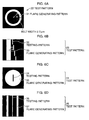
- the testing photomask 1 has test patterns 21 as shown in Fig. 4A, and each of the test patterns includes a basic structure of the combination of a testing pattern 11 and a flare generating pattern 12, the testing pattern 11 having a pattern size (here, line width) of, for example, 120 ⁇ m, and the flare generating pattern 12 surrounding the testing pattern 11 to form a light transmitting area in a ring-belt shape and having a width of, for example, 2.76 ⁇ m.
- the correlation between the open area ratio which gives an influence to the measured testing pattern 11 at the center and the distance is found by exposure under varied radius of the flare generating pattern 12.
- An Arf stepper and a positive resist are used for the exposure, and exposure only of the testing pattern 11 without any exposure of the flare generating pattern 12 is used as a reference.
- Fig. 4B shows the correlation between the radius of exposure of the flare generating pattern 12 and pattern size variation occurring in the testing pattern 11.
- the pattern size variation is represented by a difference from the reference size in the case of only the testing pattern 11 is exposed.
- the influence of local flare is given from a distant place, and an area a certain degree distance away does not undergo the size variation, so that the same size as the reference size when only the testing pattern 11 is formed is obtainable (the difference value approximates zero).
- the flare generating pattern 12 becomes closer, the influence of the local flare is given, so that a measured value (a difference value) of pattern size of the testing pattern 11 becomes larger.
- the open area ratio calculating unit 3 calculates the open area ratio of the respective divided correction areas (Step S3).
- the open area ratio influenced by the local flare in a given actual device pattern can be derived by integrating patterns proximate to each given pattern as a function of distance.
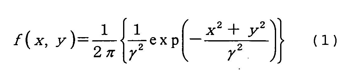
- a Gaussian function shown in the formula (1) or a triangular wave shown in the formula (2) can be used, where ⁇ represents the influence of the open area ratio.
- an exposure area having a plurality of actual device patterns is divided into a plurality of correction areas, here, divided into meshes, by arbitrary grids, and the open area ratio in each of the correction areas is calculated separately.
- a method of thus dividing the exposure area into the correction areas to approximate the pattern density is called a pattern area density map method (Japanese Patent Application Laid-open No. 2001-52999) in calculating the influence of backscatter electrons in the electron beam exposure technique.
- the dividing grid preferably has a size of about 1/10 or smaller of a range of the influence by the local flare or the like.
- Fig. 5 shows the result of calculating the influence of the local flare ( ⁇ ) with the Gaussian function shown in the formula (1) based on the test pattern as shown in Fig. 4A.
- Fig. 6A shows an example of a test pattern 22 having only a flare generating pattern 31 in a ring-belt shape forming a light transmitting area with a width of, for example, 2.7 ⁇ m
- Fig. 6B shows an example of a test pattern 23 having a belt-shaped flare generating pattern 33 and a plurality of line-shaped test patterns 32 which are apart from the flare generating pattern 33 and whose distance from the flare generating pattern 33 is made larger in sequence
- Fig. 6A shows an example of a test pattern 22 having only a flare generating pattern 31 in a ring-belt shape forming a light transmitting area with a width of, for example, 2.7 ⁇ m
- Fig. 6B shows an example of a test pattern 23 having a belt-shaped flare generating pattern 33 and a plurality of line-shaped test patterns 32 which are apart from the flare generating pattern 33 and whose distance from the flare generating pattern 33 is made larger in sequence
- Fig. 6A shows an example of a test
- FIG. 6C shows an example of a test pattern 24 having a flare generating pattern 35 which has disk shape and a line-shaped testing pattern 34 disposed in the flare generating pattern 35
- Fig. 6D shows an example of a test pattern 25 having a belt-shaped testing pattern 36 and belt-shaped flare generating patterns 37 (1 ⁇ m in width) formed to be parallel with the testing pattern 36.
- Fig. 7A to Fig.7D show the results of fitting the influence of the open area ratio with the single Gaussian function.
- Fig. 7A, Fig. 7B, Fig. 7C and Fig. 7D correspond to the cases of the test patterns in Fig. 6A, Fig. 6B, Fig. 6C and Fig. 6D respectively. It is seen that the manner of fitting differs depending on the test patterns. It is seen that there is a tendency that some place undergoes a more distant influence while the size changes near the given pattern. This implies the possibility that more precise fitting may be achieved with the plural Gaussian functions in order to faithfully express the experiment results.
- Fig. 8A to Fig. 8D show the results of fitting the influence of the open area ratio with two Gaussian functions, i.e., a double Gaussian function (1') formula below.
- ⁇ is a coefficient in entering the influence of the open area ratio into size variation.
- Fig. 8A to Fig. 8D similarly to Fig. 7A to Fig. 7D, Fig. 8A, Fig. 8B, and Fig. 8C also correspond to the cases of the test patterns in Fig. 6A, Fig. 6B, and Fig. 6C respectively.
- Fig. 9 is a chart showing the state in which exposure data is divided into square correction areas each having a size of A ⁇ A.
- an amount of size variation in an ( i + l, j + m ) th correction area distant by ( lA, mA) has an expansion caused by local flare or the like by a stepper, and thus giving an influence to size variation of an ( i, j ) th correction area.
- a contribution a l,m by local flare from the ( i + l, j + m ) th correction area distant by ( lA , mA ) is expressable by the following formula (3) in a manner that influences from the areas with A ⁇ A are integrated.
- the formula (2) is substituted in an exp part in the formula (3).
- the data correcting unit 4 expresses the correlation between the calculated open area ratio and the pattern size variation by a function (Step S4).
- a Gaussian function or a trapezoidal wave is usable.
- a value of size variation is approximated with the Gaussian function, it is expressable by the formula (5), where ⁇ is a parameter related to the size variation.
- the size in a given pattern correlates with the sum of surface integral values of the formula (4) into which the open area ratio is entered and the formula (5) accounting for the size variation. It can be calculated from a value with which the sum of the aforesaid value corresponding to the open area ratio and value corresponding to the size variation gives a certain threshold as shown in formula (6), where W is a pattern size after correction. Note that ⁇ is a coefficient in entering the influence of the open area ratio into the size variation.
- Fig. 10 shows the result of simulations on a pattern of 140 nm in pattern size, in which a value of ⁇ is intentionally changed for fitting when parameters ⁇ , ⁇ , ⁇ are made to approximate the correlation between the open area ratio and pattern size shown in Fig. 4B.
- the ⁇ value becomes larger than 80 nm, the size correction value begins to be alienated from those in a group with the ⁇ value of 70 nm or less. This implies that there exists in a given pattern size an ⁇ value that is effective in expressing the open area ratio as the pattern size, and shows that ⁇ has to be 1/2 of a target pattern size or smaller.
- a trapezoidal wave is also usable as an approximation function as shown in Fig. 11.
- the first term of the formula (6) can be expressed by the formula (7).
- ⁇ is a size difference when the open area ratio changes from 0 to 100%, i.e., to the maximum, and when an arbitrary intensity is 1/2, the size is W.
- the open area ratio in a given actual device pattern in each of the correction areas is approximated with the Gaussian, double Gaussian or the triangular wave and an amount of pattern size variation is approximated with the Gaussian or the trapezoidal wave so as to enable the correction in relation to the open area ratio, and then the procedure for extraction of the correction amount and the correction follows.
- the electron beam lithography technique there is a method of approximating forward scatter and backward scatter, which have physical meanings, with a Gaussian to correct a proximity effect in each correction area (Japanese Patent Application No. 2001-112787, Japanese Patent Application No. 2001-153233).
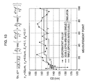
- Fig. 12 shows an evaluation result of a given pattern size when the influence of the open area ratio is approximated with the Gaussian function based on the pattern area density map method and an amount of the size variation is approximated with the Gaussian function.
- the parameters ⁇ , ⁇ , ⁇ were fitted based on the exposure result shown in Fig. 4B.
- Actual measurement values are values measured with an SEM and an Arf stepper and a positive resist were used at the time of measurement.
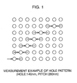
- the hole pattern shown in Fig. 1 (a pattern in which patterns each having a 140 nm via diameter are arrange at a 280 nm pitch) is used in the evaluation, and the measurement with the SEM and calculation progress from a corner of a pattern area toward the center thereof.
- the horizontal axis shows the number of measured patterns when a measurement point was shifted from the corner of the pattern area toward the center, and the vertical axis shows measured and calculated hole sizes.
- the hole size becomes larger toward the center, and it is seen that the values calculated by the method of this embodiment can account for this. This is a result of approximation of the variation amount of the pattern size with the Gaussian, but a similar result is obtained when the trapezoidal wave is used. Therefore, the fact that the size variation caused by the influence of local flare changes depending on the open area ratio can be explained by this embodiment, and the correction of the pattern size value based on this value makes it possible to obtain high precision in size.
- Fig. 13 shows the evaluation result on a given pattern size when the influence of the open area ratio is approximated with a double Gaussian function based on the pattern area density map method and an amount of size variation is approximated with a Gaussian function, the result being added to FIG. 12.
- the correction of the influence by exposure i.e., local flare is described, but the loading effect in etching that causes size variation in relation to the resist pattern density can be also corrected in a similar manner.
- the units constituting the pattern size correcting device and the steps (Steps S1 to S6 in Fig. 3A, Steps S11 to S16 in Fig. 3B, Steps S21 to S27 in Fig. 3C) of the pattern size correcting method according to the above-described embodiment are realizable by the operation of a program stored in a RAM, a ROM, or the like of a computer.
- the program and a computer-readable storage medium recording the program are included in the present invention.
- the program is recorded on a recording medium, for example, a CD-ROM, or is supplied to a computer via various kinds of transmission media.
- a storage medium recording the aforesaid program a flexible disc, a hard disc, a magnetic tape, a magneto-optic disc, a nonvolatile memory card, or the like is usable besides a CD-ROM.
- a transmission medium of the aforesaid program usable is a communication medium (a wire circuit such as an optical fiber, a wireless circuit, or the like) in a computer network (LAN, WAN such as the Internet, a radio communication network, or the like) system for supplying program information by propagating the program information as a carrier wave.
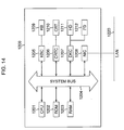
- Fig. 14 is a schematic view showing an internal structure of a typical personal user terminal device.
- 1200 denotes a computer PC.
- the PC 1200 includes a CPU 1201 which executes device controlling software stored in a ROM 1202 or a hard disc (HD) 1211 or supplied by a flexible disc drive (FD) 1212, and centrally controls each device connected to a system bus 1204.
- Patent document 1 Japanese Patent Application Laid-open No. 2001-52999
- Patent document 2 Japanese Patent Application No. 2001-112787
- Patent document 3 Japanese Patent Application No. 2001-153233 Non-patent document 1 Tae Moon Jeong, and so on (Samsung), 'Flare in Microlithographic Exposure Tools', Jpn. J. Appli. Phys. Vol. 41(2002)5113
- a pattern size correcting device and a pattern size correcting method that enable quantitative estimation of size variation occurring in a pattern exposed in lithography and easy and accurate correction of pattern size based on the estimation, thereby enabling manufacturing of an extremely reliable device.
Landscapes
- Physics & Mathematics (AREA)
- General Physics & Mathematics (AREA)
- Exposure And Positioning Against Photoresist Photosensitive Materials (AREA)
- Preparing Plates And Mask In Photomechanical Process (AREA)
Abstract
Description





Japanese Patent Application Laid-open No. 2001-52999
Japanese Patent Application No. 2001-112787
Japanese Patent Application No. 2001-153233
Tae Moon Jeong, and so on (Samsung), 'Flare in Microlithographic Exposure Tools', Jpn. J. Appli. Phys. Vol. 41(2002)5113
Claims (38)
- A pattern size correcting device for correcting size variation that occurs in an actual device pattern formed in photolithography depending on open area ratio of light transmitting areas around the actual device pattern, said device comprising:a testing photomask having a test pattern;a quantifying unit that quantifies, using said testing photomask, the size variation in the test pattern as a function of distance and in relation to the open area ratio;an open area ratio calculating unit that divides an exposure area having the plural actual device patterns into a plurality of correction areas and calculates the open area ratio of the respective correction areas; anda data correcting unit that inputs the open area ratio calculated by said open area ratio calculating unit to a result of the quantification, calculates the size variations of the actual device patterns in the respective correction areas and corrects design data of the actual device patterns based on the calculation.
- The pattern size correcting device according to claim 1, wherein the test pattern of said testing photomask has: a measuring pattern as an object of the estimation of the size variation; and a plurality of flare generating patterns that are light transmitting areas causing the size variation in the measuring pattern and whose distances from the measuring pattern are different.
- The pattern size correcting device according to claim 2, wherein said quantifying unit quantifies the size of the measuring pattern corresponding to each of the flare generating patterns in relation to the distance between the measuring pattern and each of the flare generating patterns, and based on the quantification, quantifies the size variation in relation to the open area ratio.
- The pattern size correcting device according to claim 1, wherein said open area ratio calculating unit finds area density of each of the correction areas and calculates the open area ratio by approximation calculation using a Gaussian function.
- The pattern size correcting device according to claim 1, wherein said open area ratio calculating unit finds area density of each of the correction areas and calculates the open area ratio by approximation calculation using at least two Gaussian functions.
- The pattern size correcting device according to claim 1, wherein said data correcting unit calculates the size variation of the actual device pattern caused by variation in the open area ratio, by approximation calculation using a Gaussian function.
- The pattern size correcting device according to claim 6, wherein the Gaussian function used in the calculation of the size variation by said data correcting unit has a numerical value whose value of 1/e of the Gaussian is equal to or smaller than 1/2 of a minimum pattern width included in the actual device pattern and is close to 1/2.
- The pattern size correcting device according to claim 1, wherein said data correcting unit calculates the size variation of the actual device pattern caused by variation in the open area ratio, by approximation calculation using a trapezoidal function.
- The pattern size correcting device according to claim 1, further comprising an optical proximity effect correcting unit.
- A pattern size correcting device, comprising:an open area ratio calculating unit that divides an exposure area having a plurality of actual device patterns into a plurality of correction areas and calculates open area ratio of light transmitting areas of the respective correction areas; anda data correcting unit that calculates, using the calculated open area ratio, size variations occurring in the actual device patterns in the respective correction areas and corrects design data of the actual device patterns based on the calculation.
- The pattern size correcting device according to claim 10, wherein said open area ratio calculating unit finds area density of each of the correction areas and calculates the open area ratio by approximation calculation using a Gaussian function.
- The pattern size correcting device according to claim 10, wherein said open area ratio calculating unit finds area density of each of the correction areas and calculates the open area ratio by approximation calculation using at least two Gaussian functions.
- The pattern size correcting device according to claim 10, wherein said data correcting unit calculates the size variation of the actual device pattern caused by variation in the open area ratio, by approximation calculation using a Gaussian function.
- The pattern size correcting device according to claim 13, wherein the Gaussian function used in the calculation of the size variation by said data correcting unit has a numerical value whose value of 1/e of the Gaussian is equal to or smaller than 1/2 of a minimum pattern width included in the actual device pattern and is close to 1/2.
- The pattern size correcting device according to claim 10, wherein said data correcting unit calculates the size variation of the actual device pattern caused by variation in the open area ratio, by approximation calculation using a trapezoidal function.
- The pattern size correcting device according to claim 10, further comprising an optical proximity effect correcting unit.
- A pattern size correcting method for correcting size variation that occurs in an actual device pattern formed in photolithography depending on open area ratio of light transmitting areas around the actual device pattern, said method comprising:a first step of quantifying, using a testing photomask having a test pattern, the size variation in the test pattern as a function of distance and in relation to the open area ratio;a second step of dividing an exposure area having the plural actual device patterns into a plurality of correction areas and calculating the open area ratio of the respective correction areas; anda third step of inputting the calculated open area ratio into a result of the quantification, calculating the size variations of the actual device patterns in the respective correction areas, and correcting design data of the actual device patterns based on the calculation.
- The pattern size correcting method according to claim 17, wherein the test pattern of the testing photomask has: a measuring pattern as an object of the estimation of the size variation; and a plurality of flare generating patterns that are light transmitting areas causing the size variation in the measuring pattern and whose distances from the measuring pattern are different.
- The pattern size correcting method according to claim 18, wherein in said first step, the size of the measuring pattern corresponding to each of the flare generating patterns is quantified in relation to the distance between the measuring pattern and each of the flare generating patterns, and based on the quantification, the size variation is quantified in relation to the open area ratio.
- The pattern size correcting method according to claim 17, wherein in said second step, area density of each of the correction areas is found and the open area ratio is calculated by approximation calculation using a Gaussian function.
- The pattern size correcting method according to claim 17, wherein in said second step, area density of each of the correction areas is found and the open area ratio is calculated by approximation calculation using at least two Gaussian functions.
- The pattern size correcting method according to claim 17, wherein in said third step, the size variation of the actual device pattern caused by variation in the open area ratio is calculated by approximation calculation using a Gaussian function.
- The pattern size correcting method according to claim 22, wherein the Gaussian function used in the calculation of the size variation in said third step has a numerical value whose value of 1/e of the Gaussian is equal to or smaller than 1/2 of a minimum pattern width included in the actual device pattern and is close to 1/2.
- The pattern size correcting method according to claim 17, wherein in said third step, the size variation of the actual device pattern caused by variation in the open area ratio is calculated by approximation calculation using a trapezoidal function.
- The pattern size correcting method according to claim 17, further comprising a fourth step of correcting an optical proximity effect.
- The pattern size correcting method according to claim 25, wherein said fourth step is executed before said first step, after said third step, or both before said first step and after said third step.
- A pattern size correcting method comprising:a first step of dividing an exposure area having a plurality of actual device patterns into a plurality of correction areas and calculating open area ratio of light transmitting areas of the respective correction areas; anda second step of calculating, using the calculated open area ratio, size variations occurring in the actual device patterns in the respective correction areas and correcting design data of the actual device patterns based on the calculation.
- The pattern size correcting method according to claim 27, wherein in said first step, area density of each of the correction areas is found and the open area ratio is calculated by approximation calculation using a Gaussian function.
- The pattern size correcting method according to claim 27, wherein in said first step, area density of each of the correction areas is found and the open area ratio is calculated by approximation calculation using at least two Gaussian functions.
- The pattern size correcting method according to claim 27, wherein in said second step, the size variation of the actual device pattern caused by variation in the open area ratio is calculated by approximation calculation using a Gaussian function.
- The pattern size correcting method according to claim 30, wherein the Gaussian function used in the calculation of the size variation in said second step has a numerical value whose value of 1/e of the Gaussian is equal to or smaller than 1/2 of a minimum pattern width included in the actual device pattern and is close to 1/2.
- The pattern size correcting method according to claim 27, wherein in said second step, the size variation of the actual device pattern caused by variation in the open area ratio is calculated by approximation calculation using a trapezoidal function.
- The pattern size correcting method according to claim 27, further comprising a third step of correcting an optical proximity effect.
- The pattern size correcting method according to claim 33, wherein said third step is executed before said first step, after said second step, or both before said first step and after said second step.
- A computer program product for correcting size variation that occurs in an actual device pattern formed in photolithography depending on open area ratio of light transmitting areas around the actual device pattern, said computer program product comprising:program code means for a computer to execute a first step of quantifying, using a testing photomask having a test pattern, the size variation in the test pattern as a function of distance and in relation to the open area ratio;program code means for a computer to execute a second step of dividing an exposure area having the plural actual device patterns into a plurality of correction areas and calculating the open area ratio of the respective correction areas; andprogram code means for a computer to execute a third step of inputting the calculated open area ratio into a result of the quantification, calculating the size variations of the actual device patterns in the respective correction areas, and correcting design data of the actual device patterns based on the calculation.
- A computer-readable recording medium storing a computer program product for correcting size variation that occurs in an actual device pattern formed in photolithography depending on open area ratio of light transmitting areas around the actual device pattern, the computer program product comprising:program code means for a computer to execute a first step of quantifying, using a testing photomask having a test pattern, the size variation in the test pattern as a function of distance and in relation to the open area ratio;program code means for a computer to execute a second step of dividing an exposure area having the plural actual device patterns into a plurality of correction areas and calculating the open area ratio of the respective correction areas; andprogram code means for a computer to execute a third step of inputting the calculated open area ratio into a result of the quantification, calculating the size variations of the actual device patterns in the respective correction areas, and correcting design data of the actual device patterns based on the calculation.
- A computer program product comprising:program code means for a computer to execute a first step of dividing an exposure area having a plurality of actual device patterns into a plurality of correction areas and calculating open area ratio of light transmitting areas of the respective correction areas; andprogram code means for a computer to execute a second step of calculating, using the calculated open area ratio, size variations occurring in the actual device patterns in the respective correction areas and correcting design data of the actual device patterns based on the calculation.
- A computer-readable recording medium recording a computer program product, the computer program product comprising:program code means for a computer to execute a first step of dividing an exposure area having a plurality of actual device patterns into a plurality of correction areas and calculating open area ratio of light transmitting areas of the respective correction areas; andprogram code means for a computer to execute a second step of calculating, using the calculated open area ratio, size variations occurring in the actual device patterns in the respective correction areas and correcting design data of the actual device patterns based on the calculation.
Applications Claiming Priority (5)
| Application Number | Priority Date | Filing Date | Title |
|---|---|---|---|
| JP2002224036 | 2002-07-31 | ||
| JP2002224036 | 2002-07-31 | ||
| JP2002322899A JP2004126486A (en) | 2002-07-31 | 2002-11-06 | Pattern dimension correction device and pattern dimension correction method |
| JP2002322899 | 2002-11-06 | ||
| PCT/JP2003/004616 WO2004013696A1 (en) | 2002-07-31 | 2003-04-11 | Pattern size correcting device and pattern size correcting method |
Publications (2)
| Publication Number | Publication Date |
|---|---|
| EP1553446A1 true EP1553446A1 (en) | 2005-07-13 |
| EP1553446A4 EP1553446A4 (en) | 2012-06-06 |
Family
ID=31497608
Family Applications (1)
| Application Number | Title | Priority Date | Filing Date |
|---|---|---|---|
| EP03766611A Withdrawn EP1553446A4 (en) | 2002-07-31 | 2003-04-11 | DEVICE AND METHOD FOR CORRECTING THE SIZE OF A PATTERN |
Country Status (7)
| Country | Link |
|---|---|
| US (1) | US7240307B2 (en) |
| EP (1) | EP1553446A4 (en) |
| JP (1) | JP2004126486A (en) |
| KR (1) | KR100650475B1 (en) |
| CN (1) | CN100543582C (en) |
| TW (1) | TWI236698B (en) |
| WO (1) | WO2004013696A1 (en) |
Cited By (1)
| Publication number | Priority date | Publication date | Assignee | Title |
|---|---|---|---|---|
| CN103631085A (en) * | 2012-08-29 | 2014-03-12 | 中芯国际集成电路制造(上海)有限公司 | Correction method for optical proximity correction model |
Families Citing this family (23)
| Publication number | Priority date | Publication date | Assignee | Title |
|---|---|---|---|---|
| JP4324049B2 (en) | 2004-07-23 | 2009-09-02 | 富士通マイクロエレクトロニクス株式会社 | Mask pattern correction apparatus and method, and exposure correction apparatus and method |
| KR100662961B1 (en) | 2005-12-17 | 2006-12-28 | 동부일렉트로닉스 주식회사 | Test pattern production method for optical proximity modeling data extraction |
| JP5063071B2 (en) * | 2006-02-14 | 2012-10-31 | 株式会社ニューフレアテクノロジー | Pattern creating method and charged particle beam drawing apparatus |
| JP5443548B2 (en) * | 2006-02-14 | 2014-03-19 | 株式会社ニューフレアテクノロジー | Pattern creating method and charged particle beam drawing apparatus |
| KR100801737B1 (en) * | 2006-06-28 | 2008-02-11 | 주식회사 하이닉스반도체 | Optical proximity effect correction method of semiconductor device pattern |
| JP5223197B2 (en) * | 2007-01-04 | 2013-06-26 | 富士通セミコンダクター株式会社 | Pattern measuring method and photomask inspection method |
| JP2008218577A (en) * | 2007-03-01 | 2008-09-18 | Canon Inc | Measuring apparatus, exposure apparatus, and device manufacturing method |
| JP4790649B2 (en) * | 2007-03-16 | 2011-10-12 | ルネサスエレクトロニクス株式会社 | Manufacturing method of semiconductor device |
| US8566755B2 (en) | 2007-11-26 | 2013-10-22 | Macronix International Co., Ltd. | Method of correcting photomask patterns |
| JP5322443B2 (en) * | 2008-01-21 | 2013-10-23 | ルネサスエレクトロニクス株式会社 | Mask pattern data generation method and semiconductor device manufacturing method |
| JP2009251500A (en) | 2008-04-10 | 2009-10-29 | Toshiba Corp | Method of verifying pattern, method of forming pattern, method of manufacturing semiconductor device, and program |
| JP5407623B2 (en) * | 2009-07-16 | 2014-02-05 | 富士通セミコンダクター株式会社 | Mask pattern evaluation method, mask pattern correction method, and mask pattern generator |
| JP5556505B2 (en) * | 2010-08-27 | 2014-07-23 | 富士通セミコンダクター株式会社 | Mask pattern correction method and mask pattern correction apparatus |
| RU2470336C2 (en) * | 2010-12-02 | 2012-12-20 | Открытое акционерное общество "Научно-исследовательский институт "Элпа" с опытным производством" (ОАО "НИИ "Элпа") | Method of producing contact photomask with submicron and nanometric design rules |
| JP2013125906A (en) * | 2011-12-15 | 2013-06-24 | Toshiba Corp | Flare map calculation method, flare map calculation program, and method of manufacturing semiconductor device |
| US10545020B2 (en) * | 2013-03-14 | 2020-01-28 | Applied Materials Israel, Ltd. | System, a method and a computer program product for size estimation |
| US10290092B2 (en) * | 2014-05-15 | 2019-05-14 | Applied Materials Israel, Ltd | System, a method and a computer program product for fitting based defect detection |
| KR102195588B1 (en) | 2014-09-05 | 2020-12-28 | 삼성전자주식회사 | Method of calculating a shift value of a cell contact |
| CN105824187B (en) * | 2015-01-06 | 2020-03-24 | 中芯国际集成电路制造(上海)有限公司 | Optical proximity correction method |
| CN105044941B (en) * | 2015-08-03 | 2018-01-12 | 深圳市华星光电技术有限公司 | The size detecting method of litho pattern |
| CN110033485A (en) * | 2019-04-11 | 2019-07-19 | 电子科技大学中山学院 | Python-based electronic paper aperture opening ratio calculation method and device |
| CN112305857B (en) * | 2019-07-31 | 2024-06-14 | 京东方科技集团股份有限公司 | Mask plate and preparation method thereof |
| KR102820491B1 (en) | 2020-03-25 | 2025-06-13 | 삼성디스플레이 주식회사 | Photo mask, display device and manufacturing mathod thereof |
Family Cites Families (17)
| Publication number | Priority date | Publication date | Assignee | Title |
|---|---|---|---|---|
| US5403088A (en) * | 1993-06-18 | 1995-04-04 | The Dow Chemical Company | Apparatus and method for the dispersion of minute bubbles in liquid materials for the production of polymer foams |
| JP3680425B2 (en) * | 1996-06-19 | 2005-08-10 | ソニー株式会社 | Photomask manufacturing method and method for determining electron beam irradiation correction amount for resist material |
| US6226034B1 (en) * | 1997-05-06 | 2001-05-01 | Roper Scientificomasd, Inc. | Spatial non-uniformity correction of a color sensor |
| JP4131880B2 (en) * | 1997-07-31 | 2008-08-13 | 株式会社東芝 | Mask data creation method and mask data creation apparatus |
| JP3177599B2 (en) * | 1998-06-12 | 2001-06-18 | 松下電子工業株式会社 | Pattern formation method |
| JP2000075467A (en) * | 1998-08-31 | 2000-03-14 | Matsushita Electronics Industry Corp | Photomask, its production and production of semiconductor device using same |
| JP2000323377A (en) * | 1999-05-07 | 2000-11-24 | Nikon Corp | Proximity effect correction method |
| US6610989B1 (en) | 1999-05-31 | 2003-08-26 | Fujitsu Limited | Proximity effect correction method for charged particle beam exposure |
| JP3813050B2 (en) * | 1999-05-31 | 2006-08-23 | 富士通株式会社 | Charged particle beam exposure method |
| JP3327394B2 (en) * | 1999-10-25 | 2002-09-24 | 日本電気株式会社 | Optical proximity correction method |
| US6436607B1 (en) * | 2000-03-02 | 2002-08-20 | Applied Materials, Inc. | Border modification for proximity effect correction in lithography |
| US6627356B2 (en) * | 2000-03-24 | 2003-09-30 | Kabushiki Kaisha Toshiba | Photomask used in manufacturing of semiconductor device, photomask blank, and method of applying light exposure to semiconductor wafer by using said photomask |
| JP2002075830A (en) * | 2000-08-29 | 2002-03-15 | Nikon Corp | Charged particle beam exposure method, reticle and device manufacturing method |
| EP1249734B1 (en) | 2001-04-11 | 2012-04-18 | Fujitsu Semiconductor Limited | Rectangle/lattice data conversion method for charged particle beam exposure mask pattern and charged particle beam exposure method |
| JP2002313693A (en) * | 2001-04-11 | 2002-10-25 | Fujitsu Ltd | How to create a mask pattern |
| US7382447B2 (en) * | 2001-06-26 | 2008-06-03 | Kla-Tencor Technologies Corporation | Method for determining lithographic focus and exposure |
| US6835507B2 (en) * | 2001-08-08 | 2004-12-28 | Samsung Electronics Co., Ltd. | Mask for use in measuring flare, method of manufacturing the mask, method of identifying flare-affected region on wafer, and method of designing new mask to correct for flare |
-
2002
- 2002-11-06 JP JP2002322899A patent/JP2004126486A/en active Pending
-
2003
- 2003-04-11 KR KR1020057000749A patent/KR100650475B1/en not_active Expired - Fee Related
- 2003-04-11 WO PCT/JP2003/004616 patent/WO2004013696A1/en not_active Ceased
- 2003-04-11 EP EP03766611A patent/EP1553446A4/en not_active Withdrawn
- 2003-04-11 CN CNB038170418A patent/CN100543582C/en not_active Expired - Fee Related
- 2003-04-17 TW TW092108938A patent/TWI236698B/en not_active IP Right Cessation
-
2005
- 2005-01-25 US US11/041,216 patent/US7240307B2/en not_active Expired - Lifetime
Cited By (2)
| Publication number | Priority date | Publication date | Assignee | Title |
|---|---|---|---|---|
| CN103631085A (en) * | 2012-08-29 | 2014-03-12 | 中芯国际集成电路制造(上海)有限公司 | Correction method for optical proximity correction model |
| CN103631085B (en) * | 2012-08-29 | 2016-08-31 | 中芯国际集成电路制造(上海)有限公司 | The bearing calibration of optical proximity correction model |
Also Published As
| Publication number | Publication date |
|---|---|
| CN1668979A (en) | 2005-09-14 |
| CN100543582C (en) | 2009-09-23 |
| JP2004126486A (en) | 2004-04-22 |
| US7240307B2 (en) | 2007-07-03 |
| EP1553446A4 (en) | 2012-06-06 |
| TWI236698B (en) | 2005-07-21 |
| US20050121628A1 (en) | 2005-06-09 |
| KR20050033066A (en) | 2005-04-08 |
| WO2004013696A1 (en) | 2004-02-12 |
| KR100650475B1 (en) | 2006-11-30 |
| TW200402082A (en) | 2004-02-01 |
Similar Documents
| Publication | Publication Date | Title |
|---|---|---|
| US7240307B2 (en) | Pattern size correcting device and pattern size correcting method | |
| US7473495B2 (en) | Method of creating predictive model, method of managing process steps, method of manufacturing semiconductor device, method of manufacturing photo mask, and computer program product | |
| US8372565B2 (en) | Method for optimizing source and mask to control line width roughness and image log slope | |
| US6893800B2 (en) | Substrate topography compensation at mask design: 3D OPC topography anchored | |
| US8334968B2 (en) | Recording medium storing program for determining exposure parameter, exposure method, and method of manufacturing device | |
| KR101757743B1 (en) | Flare correction method and method for fabricating EUV(Extreme Ultra Violet) mask | |
| US7601471B2 (en) | Apparatus and method for correcting pattern dimension and photo mask and test photo mask | |
| US8043772B2 (en) | Manufacturing method and manufacturing system of semiconductor device | |
| US20090019418A1 (en) | Lithography simulation method, mask pattern preparation method, semiconductor device manufacturing method and recording medium | |
| US20040023130A1 (en) | Test photomask, flare evaluation method, and flare compensation method | |
| TW201342504A (en) | Method and device for manufacturing wafer | |
| TW200900872A (en) | Method for predicting resist pattern shape, computer readable medium storing program for predicting resist pattern shape, and computer for predicting resist pattern shape | |
| CN103472672A (en) | Correction method of optical proximity correction model | |
| US8756536B2 (en) | Generation method, storage medium, and information processing apparatus | |
| TW201905967A (en) | Device manufacturing method | |
| CN117031887A (en) | Methods, equipment and media for layout marking | |
| US20190361354A1 (en) | Method and apparatus for simulation of lithography overlay | |
| JP2004163670A (en) | Exposure mask correction method and exposure management method | |
| KR100864934B1 (en) | Mask layout correction method and mask layout correction device | |
| US11699017B2 (en) | Die yield assessment based on pattern-failure rate simulation | |
| JP4317186B2 (en) | Local flare correction | |
| US7229721B2 (en) | Method for evaluating photo mask and method for manufacturing semiconductor device | |
| CN121187086B (en) | Method for performing defocus compensation on wafer, semiconductor device and related products | |
| JP4818281B2 (en) | Process management method, semiconductor device manufacturing method, photomask manufacturing method, and program | |
| CN120891694A (en) | Optical proximity effect correction methods, systems, terminals and media |
Legal Events
| Date | Code | Title | Description |
|---|---|---|---|
| PUAI | Public reference made under article 153(3) epc to a published international application that has entered the european phase |
Free format text: ORIGINAL CODE: 0009012 |
|
| 17P | Request for examination filed |
Effective date: 20041216 |
|
| AK | Designated contracting states |
Kind code of ref document: A1 Designated state(s): AT BE BG CH CY CZ DE DK EE ES FI FR GB GR HU IE IT LI LU MC NL PT SE SI SK TR |
|
| RBV | Designated contracting states (corrected) |
Designated state(s): DE FR IT |
|
| RAP1 | Party data changed (applicant data changed or rights of an application transferred) |
Owner name: FUJITSU MICROELECTRONICS LIMITED |
|
| RAP1 | Party data changed (applicant data changed or rights of an application transferred) |
Owner name: FUJITSU SEMICONDUCTOR LIMITED |
|
| RIC1 | Information provided on ipc code assigned before grant |
Ipc: G03F 1/36 20120101ALI20120404BHEP Ipc: H01L 21/027 20060101AFI20120404BHEP |
|
| A4 | Supplementary search report drawn up and despatched |
Effective date: 20120507 |
|
| 17Q | First examination report despatched |
Effective date: 20121128 |
|
| RAP1 | Party data changed (applicant data changed or rights of an application transferred) |
Owner name: FUJITSU SEMICONDUCTOR LIMITED |
|
| STAA | Information on the status of an ep patent application or granted ep patent |
Free format text: STATUS: THE APPLICATION HAS BEEN WITHDRAWN |
|
| 18W | Application withdrawn |
Effective date: 20181123 |
|
| RIC1 | Information provided on ipc code assigned before grant |
Ipc: H01L 21/027 20060101AFI20120404BHEP Ipc: G03F 1/36 20120101ALI20120404BHEP |