EP1553114A1 - Photosensitive resin composition for optical waveguide formation and optical waveguide - Google Patents
Photosensitive resin composition for optical waveguide formation and optical waveguide Download PDFInfo
- Publication number
- EP1553114A1 EP1553114A1 EP03799178A EP03799178A EP1553114A1 EP 1553114 A1 EP1553114 A1 EP 1553114A1 EP 03799178 A EP03799178 A EP 03799178A EP 03799178 A EP03799178 A EP 03799178A EP 1553114 A1 EP1553114 A1 EP 1553114A1
- Authority
- EP
- European Patent Office
- Prior art keywords
- meth
- resin composition
- acrylate
- optical waveguide
- och
- Prior art date
- Legal status (The legal status is an assumption and is not a legal conclusion. Google has not performed a legal analysis and makes no representation as to the accuracy of the status listed.)
- Granted
Links
Classifications
-
- C—CHEMISTRY; METALLURGY
- C08—ORGANIC MACROMOLECULAR COMPOUNDS; THEIR PREPARATION OR CHEMICAL WORKING-UP; COMPOSITIONS BASED THEREON
- C08F—MACROMOLECULAR COMPOUNDS OBTAINED BY REACTIONS ONLY INVOLVING CARBON-TO-CARBON UNSATURATED BONDS
- C08F220/00—Copolymers of compounds having one or more unsaturated aliphatic radicals, each having only one carbon-to-carbon double bond, and only one being terminated by only one carboxyl radical or a salt, anhydride ester, amide, imide or nitrile thereof
- C08F220/02—Monocarboxylic acids having less than ten carbon atoms; Derivatives thereof
- C08F220/10—Esters
- C08F220/12—Esters of monohydric alcohols or phenols
- C08F220/16—Esters of monohydric alcohols or phenols of phenols or of alcohols containing two or more carbon atoms
-
- G—PHYSICS
- G02—OPTICS
- G02B—OPTICAL ELEMENTS, SYSTEMS OR APPARATUS
- G02B6/00—Light guides; Structural details of arrangements comprising light guides and other optical elements, e.g. couplings
- G02B6/10—Light guides; Structural details of arrangements comprising light guides and other optical elements, e.g. couplings of the optical waveguide type
- G02B6/12—Light guides; Structural details of arrangements comprising light guides and other optical elements, e.g. couplings of the optical waveguide type of the integrated circuit kind
- G02B6/122—Basic optical elements, e.g. light-guiding paths
- G02B6/1221—Basic optical elements, e.g. light-guiding paths made from organic materials
-
- C—CHEMISTRY; METALLURGY
- C08—ORGANIC MACROMOLECULAR COMPOUNDS; THEIR PREPARATION OR CHEMICAL WORKING-UP; COMPOSITIONS BASED THEREON
- C08F—MACROMOLECULAR COMPOUNDS OBTAINED BY REACTIONS ONLY INVOLVING CARBON-TO-CARBON UNSATURATED BONDS
- C08F220/00—Copolymers of compounds having one or more unsaturated aliphatic radicals, each having only one carbon-to-carbon double bond, and only one being terminated by only one carboxyl radical or a salt, anhydride ester, amide, imide or nitrile thereof
- C08F220/02—Monocarboxylic acids having less than ten carbon atoms; Derivatives thereof
- C08F220/10—Esters
- C08F220/20—Esters of polyhydric alcohols or phenols, e.g. 2-hydroxyethyl (meth)acrylate or glycerol mono-(meth)acrylate
-
- C—CHEMISTRY; METALLURGY
- C08—ORGANIC MACROMOLECULAR COMPOUNDS; THEIR PREPARATION OR CHEMICAL WORKING-UP; COMPOSITIONS BASED THEREON
- C08F—MACROMOLECULAR COMPOUNDS OBTAINED BY REACTIONS ONLY INVOLVING CARBON-TO-CARBON UNSATURATED BONDS
- C08F222/00—Copolymers of compounds having one or more unsaturated aliphatic radicals, each having only one carbon-to-carbon double bond, and at least one being terminated by a carboxyl radical and containing at least one other carboxyl radical in the molecule; Salts, anhydrides, esters, amides, imides, or nitriles thereof
- C08F222/10—Esters
- C08F222/1006—Esters of polyhydric alcohols or polyhydric phenols
- C08F222/102—Esters of polyhydric alcohols or polyhydric phenols of dialcohols, e.g. ethylene glycol di(meth)acrylate or 1,4-butanediol dimethacrylate
-
- G—PHYSICS
- G02—OPTICS
- G02B—OPTICAL ELEMENTS, SYSTEMS OR APPARATUS
- G02B6/00—Light guides; Structural details of arrangements comprising light guides and other optical elements, e.g. couplings
- G02B6/10—Light guides; Structural details of arrangements comprising light guides and other optical elements, e.g. couplings of the optical waveguide type
- G02B6/12—Light guides; Structural details of arrangements comprising light guides and other optical elements, e.g. couplings of the optical waveguide type of the integrated circuit kind
- G02B6/13—Integrated optical circuits characterised by the manufacturing method
- G02B6/138—Integrated optical circuits characterised by the manufacturing method by using polymerisation
-
- G—PHYSICS
- G02—OPTICS
- G02B—OPTICAL ELEMENTS, SYSTEMS OR APPARATUS
- G02B6/00—Light guides; Structural details of arrangements comprising light guides and other optical elements, e.g. couplings
- G02B6/10—Light guides; Structural details of arrangements comprising light guides and other optical elements, e.g. couplings of the optical waveguide type
- G02B6/12—Light guides; Structural details of arrangements comprising light guides and other optical elements, e.g. couplings of the optical waveguide type of the integrated circuit kind
- G02B2006/12035—Materials
- G02B2006/12069—Organic material
Definitions
- the present invention relates to a photosensitive resin composition for optical waveguide formation which is used for fabricating optical circuits used in the fields of optical communications and optical information processing, and also relates to an optical waveguide fabricated by using the aforementioned composition.
- optical waveguides are the basic structural elements, for example, in optical devices for realizing high-volume information transmission of movies and dynamic images, optical computers, optoelectronic integrated circuits (OEIC), and optical integrated circuits (optical IC).
- OEIC optoelectronic integrated circuits
- optical IC optical integrated circuits
- Quartz optical waveguides and polymer optical waveguides are known as optical waveguides.
- quartz optical waveguides have an advantage of a low transmission loss.
- quartz optical waveguides have disadvantages of causing process-related problems which include a high temperature required in the processing of the manufacturing step, and difficulties encountered in the production of optical waveguides having large surface areas.
- polymer optical waveguides include easiness of processing and a large degree of freedom in material design. For this reason, the use of polymer materials such as poly(methyl methacrylate), polycarbonate and the like have been studied. However, polymer optical waveguides usually have poor heat resistance. For this reason, fluorinated polyimides that have excellent heat resistance and transmission loss have been widely researched in recent years.
- photocurable materials such as epoxy UV-curable resins having photolithographic capability, and optical waveguides using such photocurable materials have been recently suggested (for example, see claim 1 of Japanese Patent Application Laid-open (JP-A) No. H6-273631).
- the problems associated with the conventional polymer optical waveguides are that the waveguide loss in the region of a wavelength of 650-1600 nm is comparatively high, heat resistance is poor, and some of the characteristics required for the optical waveguides are unsatisfactory.
- the present invention has been created to resolve the above-described problems, and an object of the present invention is to provide a resin composition for an optical waveguide which has excellent physical properties such as waveguide loss, refractive index and heat resistance, and an optical waveguide composed of the cured product of such a composition.
- the inventors have conducted a comprehensive study to resolve the above-described problems and have found that a photosensitive resin composition, which comprises a photoradical polymerization initiator and two different (meth)acrylates having aromatic rings, is perfectly suitable as a resin for forming an optical waveguide. This finding led to the creation of the present invention.
- the present invention provides a photosensitive resin composition for optical waveguide formation, comprising:
- the photosensitive resin composition for optical waveguide formation having such a structure has excellent patterning ability during curing, and demonstrates physical properties such as a high refractive index, high heat resistance, and excellent transmission characteristic (i.e. low waveguide loss) when an optical waveguide is formed.
- the photosensitive resin composition can be preferably used as a material for forming a core layer and the like of an optical waveguide.
- the resin composition of the present invention can be so composed that the weight ratio (A/B) of the component (A) to the component (B) is, for example, 0.3 to 5.0.
- the resin composition of the present invention can be so constituted that total amount of the component (A) and the component (B) in the composition is 30 wt.% or higher.
- the resin composition of the present invention can comprises a (meth)acrylate having 3 or more (meth)acryloyl groups in a molecule.
- the resin composition of the present invention makes it possible to obtain a cured product having a refractive index of 1.54 or higher at 25°C and 824 nm.
- the resin composition of the present invention makes it possible to obtain a cured product having a glass transition temperature (Tg) of 80°C or higher.
- the present invention provides an optical waveguide which comprises a core layer, and a clad layer formed by lamination on the core layer, wherein the core layer and/or the clad layer is composed of the cured product of the aforementioned resin composition.
- the optical waveguide having the above-described structure has physical properties such as a high refractive index, high heat resistance, excellent patterning ability, and low waveguide loss.
- the present invention also provides a method for manufacturing an optical waveguide, which comprises a step of irradiating the aforementioned resin composition with radiation via a photomask and curing the resin composition.
- the resin composition of the present invention comprises the below-explained components (A)-(C) as the constituent components.
- the concept of the resin composition of the present invention includes both the liquid form prior to curing, which comprises the components (A) to (C), and the form obtained by curing the liquid composition comprising the components (A) to (C).
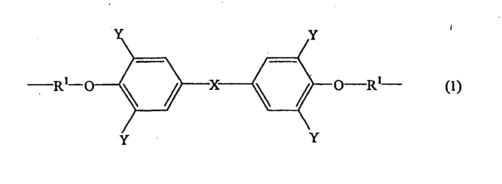
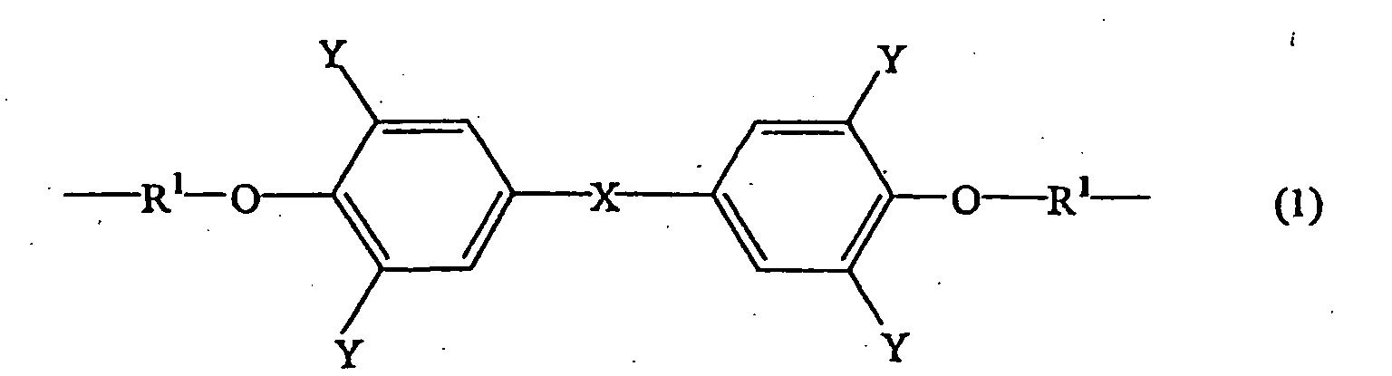
- the component (A) constituting the resin composition of the present invention is a di(meth)acrylate having the structure represented by the following general formula (1): (wherein R 1 is -(OCH 2 CH 2 ) m -, -(OCH(CH 3 )CH 2 ) m -, or -OCH 2 CH(OH)CH 2 -; X is -C(CH 3 ) 2 -, -CH 2 -, -O-, or -SO 2 -; Y is a hydrogen atom or a halogen atom; m is an integer of 0 to 4).
- examples of the halogen atom represented by Y include chlorine, bromine, iodine, and fluorine. Among them, bromine is preferred.
- component (A) examples include ethylene oxide-added bisphenol A (meth)acrylic acid ester, ethylene oxide-added tetrabromobisphenol A (meth)acrylic acid ester, propylene oxide-added bisphenol A (meth)acrylic acid ester, propylene oxide-added tetrabromobisphenol A (meth)acrylic acid ester, bisphenol A epoxy (meth)acrylate obtained by the epoxy ring opening reaction of bisphenol A diglycidyl ether and (meth)acrylic acid, tetrabromobisphenol A epoxy (meth)acrylate obtained by the epoxy ring opening reaction of tetrabromobisphenol A diglycidyl ether and (meth)acrylic acid, bisphenol F epoxy (meth)acrylate obtained by the epoxy ring opening reaction of bisphenol F diglycidyl ether and (meth)acrylic acid, and tetrabromobisphenol F epoxy (meth)acrylate obtained by the epoxy ring opening reaction of
- ethylene oxide-added bisphenol A (meth)acrylic acid ester ethylene oxide-added tetrabromobisphenol A (meth)acrylic acid ester, bisphenol A epoxy (meth)acrylate obtained by the epoxy ring opening reaction of bisphenol A diglycidyl ether and (meth)acrylic acid, and tetrabromobisphenol A epoxy (meth)acrylate are especially preferred.
- Examples of commercial products of the component (A) include Biscoat #700, #540 (manufactured by Osaka Yuki Kagaku Kogyo K. K.), Aronix M-208, M-210 (manufactured by Toa Gosei K. K.), NK Ester BPE-100, BPE-200, BPE-500, and A-BPE-4 (manufactured by Shin Nakamura Kagaku K. K.), Light Ester BP-4EA, BP-4PA, Epoxy Ester 3002M, 3002A, 3000M, 3000A (manufactured by Kyoeisha Kagaku K.
- KAYARAD R-551, R-712 manufactured by Nippon Kayaku K. K.
- BPE-4, BPE-10 manufactured by Daiichi Kogyo Seiyaku K.K.
- Ripoxy VR-77, VR-60, VR-90, SP-1506, SP-1506, SP-1507, SP1509, and SP-1563 manufactured by Showa Kobunshi K. K.
- Neopol V779, Neopol V779MA manufactured by Nippon Yupika K. K.
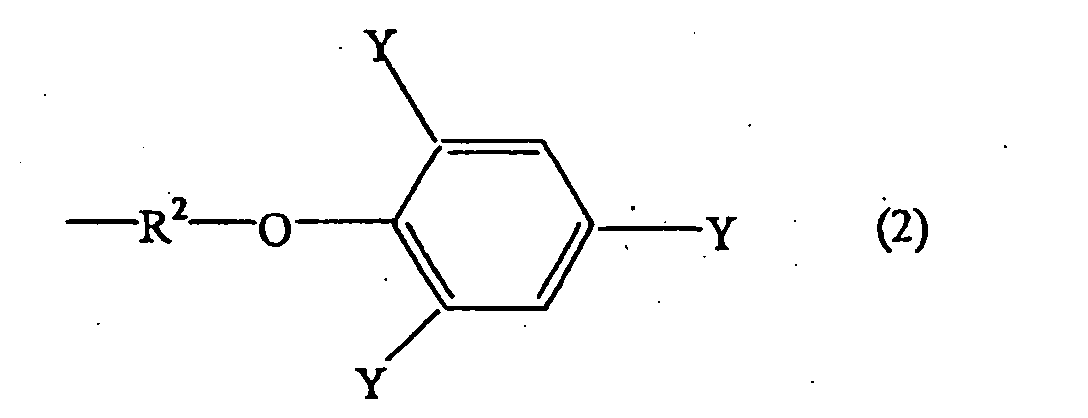
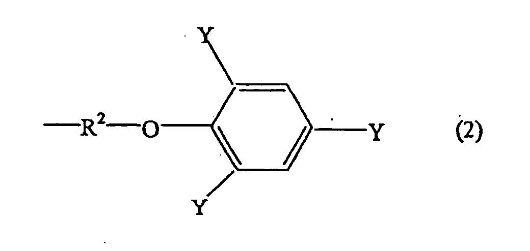
- the component (B) constituting the resin composition of the present invention is a (meth)acrylate having the structure represented by the following formula (2).
- R 2 is -(OCH 2 CH 2 ) p -, -(OCH(CH 3 )CH 2 ) p -, or -OCH 2 CH(OH)CH 2 -
- Y is a hydrogen atom, a halogen atom, Ph-C(CH 3 ) 2 -, Ph-, or an alkyl group having 1 to 20 carbon atoms
- p is an integer of 0 to 4
- Ph is a phenyl group
- examples of the halogen atom represented by Y include chlorine, bromine, iodine, and fluorine. Among them, bromine is preferred.
- Examples of the component (B) include phenoxyethyl (meth)acrylate, phenoxy-2-methylethyl (meth)acrylate, phenoxyethoxyethyl (meth)acrylate, 3-phenoxy-2-hydroxypropyl (meth)acrylate, 2-phenylphenoxyethyl (meth)acrylate, 4-phenylphenoxyethyl (meth)acrylate, 2-hydroxy-3-phenoxypropyl (meth)acrylate, p-cumyl phenol ethylene oxide modified (meth)acrylate, 2-bromophenoxyethyl (meth)acrylate, 4-bromophenoxyethyl (meth)acrylate, 2,4-dibromophenoxyethyl (meth)acrylate, 2,6-dibromophenoxyethyl (meth)acrylate, and 2,4,6-tribromophenoxyethyl (meth)acrylate.
- phenoxyethyl (meth)acrylate phenoxyethoxyethyl (meth)acrylate, (meth)acrylate of p-cumyl phenol reacted with ethylene oxide, and 2,4,6-tribromophenoxyethyl (meth)acrylate are especially preferred.
- Examples of commercial products of the component (B) include Aronix M113, M110, M101, M102, M5700, and TO-1317 (manufactured by Toa Gosei K. K.), Biscoat #192, #193, #220, 3BM (manufactured by Osaka Yuki Kagaku Kogyo K. K.), NK Ester AMP-10G, AMP-20G (manufactured by Shin-Nakamura Kagaku K. K.), Light Acrylate PO-A, P-200A, Epoxy Ester M-600A (manufactured by Kyoeisha Kagaku K. K.), and PHE, CEA, PHE-2, BR-30, BR-31, BR-31M, BR-32 (manufactured by Daiichi Kogyo Seiyaku K. K.).
- the total amount of the components (A) and (B) in the resin composition of the present invention is preferably 30 wt.% or higher, more preferably 40 wt.% or higher, and especially preferably 50 wt.% or higher. If the amount is 30 wt.% or higher, when the resin composition of the present invention is used for the core portion of an optical waveguide, a higher refractive index and a lower waveguide loss can be obtained.
- the weight ratio (A/B) of the component (A) to the component (B) in the resin composition of the present invention is preferably 0.3 to 5.0, more preferably 0.4 to 4. If this weight ratio is 0.3 or higher, the glass transition temperature of the cured product is increased and heat resistance is improved. Moreover, the core layer can be more reliably formed to the desired shape. Further, if the weight ratio is 5.0 or less, the patterning ability can be improved.
- the components (A) and (B) are preferably acrylates rather than methacrylates.
- the component (C) constituting the resin composition of the present invention is a photoradical polymerization initiator.
- the component (C) include acetophenone, acetophenone benzylketal, 1-hydroxycyclohexyl phenyl ketone, 2-benzyl-2-dimethylamino-1-(4-morpholinophenyl)-butanone-1, 2,2-dimethoxy-2-phenylacetophenone, xanthone, fluorenone, benzaldehyde, fluorine, anthraquinone, triphenylamine, carbazole, 3-methylacetophenone, 4-chlorobenzophenone, 4,4'-dimethoxybenzophenone, 4,4'-diaminobenzophenone, Michler's ketone, benzoin propyl ether, benzoin ethyl ether, benzyl dimethyl ketal, 1-(4-isopropylphenyl)-2-hydroxy-2-methyl
- Examples of commercial products of the component (C) include Irgacure 184, 369, 651, 500, 819, 907, 784, 2959, CGI1700, CGI1750, CGI11850, CG24-61, Darocur 1116, 1173 (manufactured by Ciba Specialty Chemicals Co., Ltd.), Lucirin LR8728 (manufactured by BASF Co.), and Uvecryl P36 (manufactured by UCB Co.).
- the component (C) can be used alone, or can be used in combination of two or more thereof to improve the patterning ability.
- the weight ratio of the component (C) in the resin composition of the present invention is usually 0.01 to 10 wt.%, preferably 0.1 to 7 wt.%.
- the weight ratio is 10 wt.% or less, curing characteristic, transmission characteristic, patterning ability, and handleability can be improved.
- the weight ratio is 0.01 wt.% or more, patterning ability and mechanical characteristics of the cured product can be improved, and the decrease in curing rate can be prevented.
- a compound having a (meth)acryloyl group or vinyl group (sometimes referred to hereinbelow as "unsaturated monomer” with the proviso that compounds identical to the components (A) and (B) are excluded) can be used as an optional component in addition to the components (A) and (B).
- a (meth)acrylate having three or more (meth)acryloyl groups is preferably used.
- Examples of the (meth)acrylate having three or more (meth)acryloyl groups include (meth)acrylates of polyhydric alcohols having three or more hydroxyl groups.
- Examples of such (meth)acrylates include trimethylolpropane tri(meth)acrylate, pentaerythritol tri(meth)acrylate, trimethylolpropane trioxyethyl (meth)acrylate, tris(2-acryloyloxyethyl)isocyanurate, and pentaerythritol polyacrylate. These compounds may be used individually or in combinations of two or more thereof.
- Examples of commercial products of the (meth)acrylate having three or more (meth)acryloyl groups include Aronix M305, M309, M310, M315, M320, M350, M360, and M408 (manufactured by Toa Gosei K. K.), Biscoat #295, #300, #360, GPT, 3PA, #400 (manufactured by Osaka Yuki Kagaku Kogyo K. K.), NK Ester TMPT, A-TMPT, A-TMM-3, A-TMM-3L, A-TMMT (manufactured by Shin-Nakamura Kagaku K.
- Examples of other unsaturated monomers include vinyl monomers such as N-vinyl pyrrolidone, N-vinyl caprolactam, vinyl imidazole, and vinyl pyridine; isobornyl (meth)acrylate, bornyl (meth)acrylate, tricyclodecanyl (meth)acrylate, dicyclopentanyl (meth)acrylate, dicyclopentenyl (meth)acrylate, cyclohexyl (meth)acrylate, benzyl (meth)acrylate, 4-butylcyclohexyl (meth)acrylate, acryloyl morpholine, 2-hydroxyethyl (meth)acrylate, 2-hydroxypropyl (meth)acrylate, 2-hydroxybutyl (meth)acrylate, methyl (meth)acrylate, ethyl (meth)acrylate, propyl (meth)acrylate, isopropyl (meth)acrylate, butyl (meth)acrylate, amy
- Examples of an unsaturated monomer having two (meth)acryloyl groups or vinyl groups include alkyldioldiacrylates such as 1,4-butanedioldiacrylate, 1,6-hexanedioldiacrylate and 1,9-nonanedioldiacrylate, polyalkylene glycol diacrylates such as ethylene glycol di(meth)acrylate, tetraethylene glycol diacrylate, and tripropylene glycol diacrylate, neopentylglycol di(meth)acrylate, and tricyclodecane methanol diacrylate.
- alkyldioldiacrylates such as 1,4-butanedioldiacrylate, 1,6-hexanedioldiacrylate and 1,9-nonanedioldiacrylate
- polyalkylene glycol diacrylates such as ethylene glycol di(meth)acrylate, tetraethylene glycol diacrylate, and tripropylene glycol diacrylate
- Examples of commercial products of those compounds include Aronix M120, M-150, M-156, M-215, M-220, M-225, M-240, M-245, and M-270 (manufactured by Toa Gosei K. K.), AIB, TBA, LA, LTA, STA, Biscoat #155, IBXA, Biscoat #158, #190, #150, #320, HEA, HPA, Biscoat #2000, #2100, DMA, Biscoat #195, #230, #260, #215, #335HP, #310HP, #310HG, #312 (manufactured by Osaka Yuki Kagaku Kogyo K.
- An oligomer or polymer such as polyurethane (meth)acrylate, polyester (meth)acrylate, and polyepoxy (meth)acrylate may be additionally blended with the resin composition of the present invention.
- a photosensitizer can be additionally blended with the resin composition of the present invention.
- photosensitizers examples include triethylamine, diethylamine, N-methyldiethanolamine, ethanolamine, 4-dimethylaminobenzoic acid, 4-dimethylaminobenzoic acid methyl, 4-dimethylaminobenzoic acid ethyl, and 4-dimethylaminobenzoic acid isoamyl.
- examples of commercial products of photosensitizers include Ubecryl P102, 103, 104, 105 (manufactured by UCB Co.).
- additives examples include antioxidants, UV absorbers, photostabilizers, silane coupling agents, surface modification agents, thermal polymerization inhibitors, leveling agents, surfactants, colorants, preservatives, plasticizers, lubricants, solvents, fillers, antiaging agents, wetting improving agents, and parting agents.
- antioxidants examples include Irganox 1010, 1035, 1076, 1222 (manufactured by Ciba Specialty Chemicals), Antigen P, 3C, FR, GA-80 (manufactured by Sumitomo Kagaku Kogyo K. K.).
- UV absorbers examples include Tinuvin P, 234, 320, 326, 327, 328, 329, 213 (manufactured by Ciba Specialty Chemicals), Seesorb 102, 103, 110, 501, 202, 712, 704 (manufactured by Shipro Kasei K. K.).
- Examples of commercial products of photostabilizers include Tinuvin 292, 144, 622LD (manufactured by Ciba Specialty Chemicals), Sanol LS770 (Sankyo K. K.), Sumisorb TM-061 (Sumitomo Kagaku Kogyo K. K.).
- silane coupling agents include ⁇ -aminopropyltriethoxysilane, ⁇ -mercaptopropyltrimethoxysilane, and ⁇ -methacryloxypropyltrimethoxysilane.
- examples of commercial products include SH6062, 6030 (manufactured by Toray Dow Corning Silicone Co.), KBE903, 603, 403 (manufactured by Shin-Etsu Kagaku Kogyo K. K.).
- Examples of surface modification agents include silicone additives such as dimethylsiloxane polyether.
- Examples of commercial products include DC-57, DC-190 (manufactured by Dow Corning Co.), SH-28PA, SH-29PA, SH-30PA, SH190 (manufactured by Toray Dow Corning Silicone Co.), KF351, KF352, KF353, KF354 (manufactured by Shin-Etsu Kagaku Kogyo K. K.), L-700, L-7002, L-7500, FK-024-90 (manufactured by Nippon Unicar K. K.).
- Examples of commercial products of parting agents include PRISURF A208F (manufactured by Daiichi Kogyo Seiyaku K. K.).
- the resin composition of the present invention can be manufactured by mixing the aforementioned components by the usual method.
- the viscosity of the resin composition of the present invention that is thus prepared is 100-20,000 cp/25°C, preferable 300-10,000 cp/25°C, more preferably 400-5,000 cp/25°C. If the viscosity is too high, coating non-uniformity or waving occurs when the resin composition is coated on a substrate, or the patterning ability is degraded and the designed shape cannot be obtained when a core layer is formed. Conversely, if the viscosity is too low, the desired film thickness is difficult to obtain. Moreover, the patterning ability is sometimes degraded.
- the cured product of the resin composition of the present invention that is obtained by curing with radiation preferably has the following properties.
- the refractive index at 25°C and a wavelength of 824 nm is preferably 1.54 or more, more preferably 1.55 or more. If the refractive index is less than 1.54, when a waveguide is formed by using the resin composition of the present invention for the core layer, the desired transmission loss sometimes cannot be obtained.
- the cured product of the resin composition of the present invention preferably has a glass transition temperature of 80°C or higher, more preferably 90°C or higher. If the glass transition temperature is less than 80°C, a sufficient heat resistance of the optical waveguide sometimes cannot be ensured.
- the "glass transition temperature” as referred to herein is defined as the temperature at which the loss tangent at an oscillation frequency of 10 Hz exhibits a maximum value in the resonance-type apparatus for measuring dynamic viscoelasticity.
- Liquid curable compositions were obtained by mixing the components described in Table 1 and conducting stirring for one hour, while controlling the temperature at 50-60°C.
- Table 1 the amounts of the components are described as parts by weight.
- the refractive index at 824 nm was measured by the following method. First, a resin composition layer was formed by coating a liquid curable composition to a thickness of 7 ⁇ m on a silicon wafer substrate having a thickness of 4 inches by using a spin coater, while adjusting the rotation speed and time. Then, the resin composition layer was irradiated from a mask aligner with UV rays at 1.0 J/cm 2 in a nitrogen atmosphere, and a cured film was obtained. Then, the refractive index (824 nm, 25°C) of the cured film was measured by using a prism coupler manufactured by Nippon Metricon Co.
- a resin composition layer was formed by coating a resin composition to a thickness of 60 ⁇ m on a glass substrate by using an applicator. Then, the resin composition layer was irradiated with UV rays at 1.0 J/cm 2 by using a conveyor-type UV irradiation apparatus in a nitrogen atmosphere, and a cured film was obtained. Then, the dependence of the loss tangent of the cured film on temperature was measured by using a resonance-type apparatus for measuring dynamic viscoelasticity, while applying oscillations having an oscillation frequency of 10 Hz. The glass transition temperature was defined as the temperature at which the maximum value of the loss target was obtained.
- a resin composition layer was formed by coating a liquid curable composition to a thickness of 50 ⁇ m on a silicon wafer substrate having a thickness of 4 inches by using a spin coater, while adjusting the rotation speed and time. Then, the resin composition layer was irradiated from a mask aligner with UV rays at 1.0 J/cm 2 in an air atmosphere via a photomask having a branch-free and linear shape and having a width of 50 ⁇ m. The resin composition was then developed for 3 minutes by using acetone, and the substrate was heated for 10 minutes in an oven having a fixed temperature of 70°C.
- the pattern obtained was observed under an optical microscope.
- the case in which the target core shape (50 ⁇ m ⁇ 1 ⁇ m) was obtained was denoted by "o ⁇ "
- the case in which the shape was within a range of 50 ⁇ m ⁇ 2 ⁇ m was denoted by "O”
- the case in which the shape was outside the range 50 ⁇ m ⁇ 2 ⁇ m was denoted by " ⁇ ”.
- the irradiated coated layer was developed for 3 minutes by using acetone, and the substrate was heated for 10 minutes in an oven having a fixed temperature of 70°C. Then, the ELC2500 (Clear) was again coated on the substrate to a thickness of 50 ⁇ m, and the substrate was irradiated with UV rays to obtain a channel waveguide.
- the end surface of the waveguide was cleaved and cut, light having a wavelength of 850 nm was introduced via a multimode fiber (diameter: 50 ⁇ m), and the waveguide loss was measured by a cut-back method.
- the measurement method was implemented by conducting 4-point measurements at an interval of 1 cm in a 5 cm-length portion of the waveguide.
- the light intensity obtained was plotted against the waveguide length, and the loss value was calculated from the inclination thereof.
- the case in which the loss value obtained was 0.5 dB/cm or less was denoted by "O”
- the case in which it was higher than 0.5 dB/cm was denoted by " ⁇ ".
- the resin composition of the present invention (Examples 1 to 7) has excellent patterning ability when a cured product is formed, and demonstrates excellent refractive index, heat resistance, and transmission characteristic (low waveguide loss) when an optical waveguide is formed.
- Comparative Example 1 because component (A) is not present, heat resistance is poor. In Comparative Example 2, because component (B) is not present, patterning ability is poor. In Comparative Example 3, because components (A) and (B) are not present, patterning ability and transmission characteristic are poor.
Landscapes
- Physics & Mathematics (AREA)
- Chemical & Material Sciences (AREA)
- Engineering & Computer Science (AREA)
- Medicinal Chemistry (AREA)
- Polymers & Plastics (AREA)
- Organic Chemistry (AREA)
- Health & Medical Sciences (AREA)
- Microelectronics & Electronic Packaging (AREA)
- Chemical Kinetics & Catalysis (AREA)
- General Physics & Mathematics (AREA)
- Optics & Photonics (AREA)
- Addition Polymer Or Copolymer, Post-Treatments, Or Chemical Modifications (AREA)
- Optical Integrated Circuits (AREA)
- Macromonomer-Based Addition Polymer (AREA)
Abstract

Description


Claims (8)
- A photosensitive resin composition for optical waveguide formation, comprising:(A) a di(meth)acrylate having the structure represented by the following general formula (1):(wherein R1 is -(OCH2CH2)m-, -(OCH(CH3)CH2)m-, or -OCH2CH (OH) CH2-; X is -C(CH3)2-, -CH2-,-O-, or -SO2-; Y is a hydrogen atom or a halogen atom; m is an integer of 0 to 4);
 (B) a mono(meth)acrylate having the structure represented by the following general formula (2):(wherein R2 is -(OCH2CH2)p-, -(OCH(CH3)CH2)p-, or -OCH2CH(OH)CH2-; Y is a hydrogen atom, a halogen atom, Ph-C(CH3)2-, Ph-, or an alkyl group having 1 to 20 carbon atoms; p is an integer of 0 to 4; Ph is a phenyl group);
 (C) a photoradical polymerization initiator.
 - The photosensitive resin composition for optical waveguide formation according to claim 1, wherein the weight ratio (A/B) of said component (A) to said component (B) is 0.3 to 5.0.
- The photosensitive resin composition for optical waveguide formation according to claim 1 or 2, wherein the total amount of said component (A) and said component (B) in said resin composition is 30 wt.% or higher.
- The photosensitive resin composition for optical waveguide formation according to any one of claims 1 to 3, comprising a (meth)acrylate having 3 or more (meth)acryloyl groups in a molecule.
- The photosensitive resin composition for optical waveguide formation according to any one of claims 1 to 4, wherein the refractive index of the cured product of said resin composition at 25°C and 824 nm is 1.54 or higher.
- The photosensitive resin composition for optical waveguide formation according to any one of claims 1 to 5, wherein the glass transition temperature (Tg) of the cured product of said resin composition is 80°C or higher.
- An optical waveguide comprising a core layer, and a clad layer formed by lamination on said core layer, wherein said core layer and/or said clad layer is composed of the cured product of the resin composition of any one of claims 1 to 6.
- A method for manufacturing an optical waveguide, comprising a step of irradiating the resin composition of any one of claims 1 to 6 with radiation via a photomask and curing said resin composition.
Applications Claiming Priority (9)
| Application Number | Priority Date | Filing Date | Title |
|---|---|---|---|
| JP2002294148 | 2002-10-07 | ||
| JP2002294148 | 2002-10-07 | ||
| JP2003007477 | 2003-01-15 | ||
| JP2003007477 | 2003-01-15 | ||
| JP2003067039 | 2003-03-12 | ||
| JP2003067039 | 2003-03-12 | ||
| JP2003175696A JP4222120B2 (en) | 2002-10-07 | 2003-06-20 | Photosensitive resin composition for optical waveguide formation and optical waveguide |
| JP2003175696 | 2003-06-20 | ||
| PCT/JP2003/012479 WO2004031251A1 (en) | 2002-10-07 | 2003-09-30 | Photosensitive resin composition for optical waveguide formation and optical waveguide |
Publications (3)
| Publication Number | Publication Date |
|---|---|
| EP1553114A1 true EP1553114A1 (en) | 2005-07-13 |
| EP1553114A4 EP1553114A4 (en) | 2005-10-12 |
| EP1553114B1 EP1553114B1 (en) | 2007-07-11 |
Family
ID=32074568
Family Applications (1)
| Application Number | Title | Priority Date | Filing Date |
|---|---|---|---|
| EP03799178A Expired - Lifetime EP1553114B1 (en) | 2002-10-07 | 2003-09-30 | Photosensitive resin composition for optical waveguide formation and optical waveguide |
Country Status (10)
| Country | Link |
|---|---|
| US (1) | US7376328B2 (en) |
| EP (1) | EP1553114B1 (en) |
| JP (1) | JP4222120B2 (en) |
| KR (1) | KR20050062595A (en) |
| CN (1) | CN1300199C (en) |
| AU (1) | AU2003266706A1 (en) |
| CA (1) | CA2498188A1 (en) |
| DE (1) | DE60314897T2 (en) |
| TW (1) | TW200422308A (en) |
| WO (1) | WO2004031251A1 (en) |
Cited By (1)
| Publication number | Priority date | Publication date | Assignee | Title |
|---|---|---|---|---|
| GB2459505A (en) * | 2008-04-25 | 2009-10-28 | Dublin Inst Of Technology | Optical component fabrication by depositing a polymerisation activator pattern |
Families Citing this family (14)
| Publication number | Priority date | Publication date | Assignee | Title |
|---|---|---|---|---|
| JP2004175866A (en) * | 2002-11-26 | 2004-06-24 | Nippon Kayaku Co Ltd | Adhesive composition for optical disk, cured product and article |
| KR100725023B1 (en) * | 2006-10-16 | 2007-06-07 | 제일모직주식회사 | Resin composition containing cardo resin, and manufacturing method by pattern, color filter using same |
| CN101528781B (en) * | 2006-11-10 | 2012-05-16 | 东丽株式会社 | Paste composition for light guide and light guide utilizing the same |
| JP5115057B2 (en) * | 2007-06-29 | 2013-01-09 | Jsr株式会社 | Film-shaped optical waveguide and photosensitive resin composition for film-shaped optical waveguide |
| JP4544370B2 (en) * | 2008-10-28 | 2010-09-15 | Jsr株式会社 | Radiation-sensitive resin composition, interlayer insulating film and microlens, and production method thereof |
| CN102436142B (en) | 2010-09-29 | 2013-11-06 | 第一毛织株式会社 | Black photosensitive resin composition and light blocking layer using the same |
| KR101367253B1 (en) | 2010-10-13 | 2014-03-13 | 제일모직 주식회사 | Photosensitive resin composition and black matrix using the same |
| KR101486560B1 (en) | 2010-12-10 | 2015-01-27 | 제일모직 주식회사 | Photosensitive resin composition and black matrix using the same |
| KR101453769B1 (en) | 2010-12-24 | 2014-10-22 | 제일모직 주식회사 | Photosensitive resin composition and color filter using the same |
| KR101344786B1 (en) | 2011-12-02 | 2013-12-26 | 제일모직주식회사 | Photosensitive resin composition for color filter comprising the same and color filter using the same |
| KR20140076320A (en) | 2012-12-12 | 2014-06-20 | 제일모직주식회사 | Photosensitive resin composition and black spacer using the same |
| JP6274498B2 (en) * | 2013-11-08 | 2018-02-07 | 日東電工株式会社 | Photosensitive resin composition for optical waveguide, photocurable film for forming optical waveguide core layer, optical waveguide using the same, mixed flexible printed wiring board for optical / electrical transmission |
| KR101890899B1 (en) * | 2015-10-21 | 2018-08-22 | 닛산 가가쿠 가부시키가이샤 | Composition for optical waveguide formation |
| JP7649747B2 (en) * | 2019-09-12 | 2025-03-21 | マクセル株式会社 | Resin composition for photopolymerization, modeling material composition, photocured product thereof, and photopolymerization composition set |
Family Cites Families (17)
| Publication number | Priority date | Publication date | Assignee | Title |
|---|---|---|---|---|
| JPS5119203A (en) * | 1974-08-09 | 1976-02-16 | Hitachi Ltd | Konatsutaabinno seigyosochi |
| JPS60202110A (en) * | 1984-03-26 | 1985-10-12 | Showa Denko Kk | Composition for high-refractive index resin |
| GB2195643B (en) * | 1986-07-21 | 1990-08-15 | Yokohama Rubber Co Ltd | Uv-curable resin compositions |
| JPH0643467B2 (en) * | 1987-12-08 | 1994-06-08 | 呉羽化学工業株式会社 | Method of manufacturing optical material |
| JPH01161038A (en) * | 1987-12-18 | 1989-06-23 | Nippon Kayaku Co Ltd | Resin composition and solder resist resin composition |
| JPH01299807A (en) * | 1988-05-26 | 1989-12-04 | Matsushita Electric Works Ltd | Curable resin composition and optical waveguide using it as core material |
| JPH0331309A (en) * | 1989-06-27 | 1991-02-12 | Matsushita Electric Works Ltd | Composition for preparing resin having high refractive index |
| DE4010784C2 (en) | 1990-04-04 | 1994-11-03 | Bayer Ag | Thermoset terpolymers and their use for the production of optical molded parts |
| US5263111A (en) * | 1991-04-15 | 1993-11-16 | Raychem Corporation | Optical waveguide structures and formation methods |
| JPH05119203A (en) * | 1991-10-24 | 1993-05-18 | Fujitsu Ltd | Microoptical lens and production of optical waveguide |
| JP3211108B2 (en) * | 1992-06-25 | 2001-09-25 | チッソ株式会社 | Photosensitive resin composition |
| US5616630A (en) * | 1993-02-05 | 1997-04-01 | Lord Corporation | Ester/urethane acrylate hybrid oligomers |
| JPH06273631A (en) | 1993-03-18 | 1994-09-30 | Nippon Telegr & Teleph Corp <Ntt> | Optical waveguide |
| US6005137A (en) * | 1997-06-10 | 1999-12-21 | 3M Innovative Properties Company | Halogenated acrylates and polymers derived therefrom |
| JP3867409B2 (en) * | 1998-08-25 | 2007-01-10 | Jsr株式会社 | Manufacturing method of optical waveguide |
| US6166156A (en) * | 1998-11-12 | 2000-12-26 | Wu; Chengjiu | Method for making photocurable halofluorinated acrylates |
| JP3985129B2 (en) * | 2001-04-25 | 2007-10-03 | 信越化学工業株式会社 | Electron beam curable coating for optical fiber and method for curing the same |
-
2003
- 2003-06-20 JP JP2003175696A patent/JP4222120B2/en not_active Expired - Fee Related
- 2003-09-30 CA CA002498188A patent/CA2498188A1/en not_active Abandoned
- 2003-09-30 DE DE60314897T patent/DE60314897T2/en not_active Expired - Lifetime
- 2003-09-30 CN CNB038088894A patent/CN1300199C/en not_active Expired - Fee Related
- 2003-09-30 AU AU2003266706A patent/AU2003266706A1/en not_active Abandoned
- 2003-09-30 EP EP03799178A patent/EP1553114B1/en not_active Expired - Lifetime
- 2003-09-30 US US10/527,547 patent/US7376328B2/en not_active Expired - Fee Related
- 2003-09-30 KR KR1020057005902A patent/KR20050062595A/en not_active Ceased
- 2003-09-30 WO PCT/JP2003/012479 patent/WO2004031251A1/en not_active Ceased
- 2003-10-06 TW TW092127694A patent/TW200422308A/en unknown
Cited By (1)
| Publication number | Priority date | Publication date | Assignee | Title |
|---|---|---|---|---|
| GB2459505A (en) * | 2008-04-25 | 2009-10-28 | Dublin Inst Of Technology | Optical component fabrication by depositing a polymerisation activator pattern |
Also Published As
| Publication number | Publication date |
|---|---|
| WO2004031251A1 (en) | 2004-04-15 |
| TW200422308A (en) | 2004-11-01 |
| EP1553114B1 (en) | 2007-07-11 |
| KR20050062595A (en) | 2005-06-23 |
| DE60314897D1 (en) | 2007-08-23 |
| EP1553114A4 (en) | 2005-10-12 |
| CN1300199C (en) | 2007-02-14 |
| AU2003266706A1 (en) | 2004-04-23 |
| CN1646586A (en) | 2005-07-27 |
| US20060008222A1 (en) | 2006-01-12 |
| US7376328B2 (en) | 2008-05-20 |
| DE60314897T2 (en) | 2008-03-13 |
| CA2498188A1 (en) | 2004-04-15 |
| JP2004334152A (en) | 2004-11-25 |
| JP4222120B2 (en) | 2009-02-12 |
Similar Documents
| Publication | Publication Date | Title |
|---|---|---|
| US7376328B2 (en) | Photosensitive resin composition for optical waveguide formation and optical waveguide | |
| US20050256219A1 (en) | Photocurable resin composition and optical component | |
| EP1014113A2 (en) | Photo curable resin composition and optical parts | |
| JP2004333902A (en) | Radiation curable resin composition for optical member and optical member | |
| KR101605282B1 (en) | Photo-curable composition and patterning method using the same | |
| KR101130021B1 (en) | Photocurable composition and optical part | |
| JP4552306B2 (en) | Photocurable resin composition and optical member | |
| JP2000239333A (en) | Photocurable resin composition and optical member | |
| JP4192065B2 (en) | Polymer optical waveguide | |
| CN1957046B (en) | Photocurable composition and optical part | |
| JP4151508B2 (en) | Photosensitive resin composition for optical waveguide and optical waveguide | |
| JP2008116971A (en) | Optical waveguide | |
| JP4228707B2 (en) | Photocurable composition and optical member | |
| JP3904027B2 (en) | Radiation curable resin composition for optical member and optical member | |
| JP2006152105A (en) | Photocurable resin composition and optical member | |
| JP2008275847A (en) | Polymer optical waveguide | |
| JP4710596B2 (en) | Radiation curable resin composition for optical member and optical member | |
| JP2008247849A (en) | Novel sulfur-containing ethylenically unsaturated group-containing compound, radiation curable composition and cured product | |
| WO2006068465A1 (en) | Radiation-curable resin optical member forming composition and optical member |
Legal Events
| Date | Code | Title | Description |
|---|---|---|---|
| PUAI | Public reference made under article 153(3) epc to a published international application that has entered the european phase |
Free format text: ORIGINAL CODE: 0009012 |
|
| 17P | Request for examination filed |
Effective date: 20050309 |
|
| AK | Designated contracting states |
Kind code of ref document: A1 Designated state(s): AT BE BG CH CY CZ DE DK EE ES FI FR GB GR HU IE IT LI LU MC NL PT RO SE SI SK TR |
|
| AX | Request for extension of the european patent |
Extension state: AL LT LV MK |
|
| A4 | Supplementary search report drawn up and despatched |
Effective date: 20050825 |
|
| DAX | Request for extension of the european patent (deleted) | ||
| RBV | Designated contracting states (corrected) |
Designated state(s): DE FR GB |
|
| 17Q | First examination report despatched |
Effective date: 20051024 |
|
| GRAP | Despatch of communication of intention to grant a patent |
Free format text: ORIGINAL CODE: EPIDOSNIGR1 |
|
| GRAS | Grant fee paid |
Free format text: ORIGINAL CODE: EPIDOSNIGR3 |
|
| GRAA | (expected) grant |
Free format text: ORIGINAL CODE: 0009210 |
|
| AK | Designated contracting states |
Kind code of ref document: B1 Designated state(s): DE FR GB |
|
| REG | Reference to a national code |
Ref country code: GB Ref legal event code: FG4D |
|
| REF | Corresponds to: |
Ref document number: 60314897 Country of ref document: DE Date of ref document: 20070823 Kind code of ref document: P |
|
| ET | Fr: translation filed | ||
| PLBE | No opposition filed within time limit |
Free format text: ORIGINAL CODE: 0009261 |
|
| STAA | Information on the status of an ep patent application or granted ep patent |
Free format text: STATUS: NO OPPOSITION FILED WITHIN TIME LIMIT |
|
| 26N | No opposition filed |
Effective date: 20080414 |
|
| REG | Reference to a national code |
Ref country code: FR Ref legal event code: PLFP Year of fee payment: 14 |
|
| PGFP | Annual fee paid to national office [announced via postgrant information from national office to epo] |
Ref country code: DE Payment date: 20160921 Year of fee payment: 14 Ref country code: GB Payment date: 20160920 Year of fee payment: 14 |
|
| PGFP | Annual fee paid to national office [announced via postgrant information from national office to epo] |
Ref country code: FR Payment date: 20160921 Year of fee payment: 14 |
|
| REG | Reference to a national code |
Ref country code: DE Ref legal event code: R119 Ref document number: 60314897 Country of ref document: DE |
|
| GBPC | Gb: european patent ceased through non-payment of renewal fee |
Effective date: 20170930 |
|
| REG | Reference to a national code |
Ref country code: FR Ref legal event code: ST Effective date: 20180531 |
|
| PG25 | Lapsed in a contracting state [announced via postgrant information from national office to epo] |
Ref country code: DE Free format text: LAPSE BECAUSE OF NON-PAYMENT OF DUE FEES Effective date: 20180404 Ref country code: GB Free format text: LAPSE BECAUSE OF NON-PAYMENT OF DUE FEES Effective date: 20170930 |
|
| PG25 | Lapsed in a contracting state [announced via postgrant information from national office to epo] |
Ref country code: FR Free format text: LAPSE BECAUSE OF NON-PAYMENT OF DUE FEES Effective date: 20171002 |