EP1551046A2 - Digital wake-up signal from switch transition of two analog signals - Google Patents
Digital wake-up signal from switch transition of two analog signals Download PDFInfo
- Publication number
- EP1551046A2 EP1551046A2 EP04106378A EP04106378A EP1551046A2 EP 1551046 A2 EP1551046 A2 EP 1551046A2 EP 04106378 A EP04106378 A EP 04106378A EP 04106378 A EP04106378 A EP 04106378A EP 1551046 A2 EP1551046 A2 EP 1551046A2
- Authority
- EP
- European Patent Office
- Prior art keywords
- switch
- contactor
- signal
- wake
- traces
- Prior art date
- Legal status (The legal status is an assumption and is not a legal conclusion. Google has not performed a legal analysis and makes no representation as to the accuracy of the status listed.)
- Granted
Links
- 230000007704 transition Effects 0.000 title description 13
- 230000007274 generation of a signal involved in cell-cell signaling Effects 0.000 claims description 9
- 238000000034 method Methods 0.000 claims description 4
- 230000004044 response Effects 0.000 claims description 3
- 230000002618 waking effect Effects 0.000 claims description 2
- 101100063432 Caenorhabditis elegans dim-1 gene Proteins 0.000 description 15
- 230000008859 change Effects 0.000 description 6
- 238000005286 illumination Methods 0.000 description 5
- 238000010276 construction Methods 0.000 description 3
- 238000010586 diagram Methods 0.000 description 3
- 230000000712 assembly Effects 0.000 description 2
- 238000000429 assembly Methods 0.000 description 2
- 239000004020 conductor Substances 0.000 description 2
- 230000003068 static effect Effects 0.000 description 2
- RYGMFSIKBFXOCR-UHFFFAOYSA-N Copper Chemical compound [Cu] RYGMFSIKBFXOCR-UHFFFAOYSA-N 0.000 description 1
- 229910000881 Cu alloy Inorganic materials 0.000 description 1
- 230000004913 activation Effects 0.000 description 1
- 238000006243 chemical reaction Methods 0.000 description 1
- 229910052802 copper Inorganic materials 0.000 description 1
- 239000010949 copper Substances 0.000 description 1
- 239000011810 insulating material Substances 0.000 description 1
- 230000004048 modification Effects 0.000 description 1
- 238000012986 modification Methods 0.000 description 1
- 230000000737 periodic effect Effects 0.000 description 1
- 239000007787 solid Substances 0.000 description 1
Images


Classifications
-
- H—ELECTRICITY
- H01—ELECTRIC ELEMENTS
- H01H—ELECTRIC SWITCHES; RELAYS; SELECTORS; EMERGENCY PROTECTIVE DEVICES
- H01H19/00—Switches operated by an operating part which is rotatable about a longitudinal axis thereof and which is acted upon directly by a solid body external to the switch, e.g. by a hand
- H01H19/54—Switches operated by an operating part which is rotatable about a longitudinal axis thereof and which is acted upon directly by a solid body external to the switch, e.g. by a hand the operating part having at least five or an unspecified number of operative positions
- H01H19/56—Angularly-movable actuating part carrying contacts, e.g. drum switch
- H01H19/58—Angularly-movable actuating part carrying contacts, e.g. drum switch having only axial contact pressure, e.g. disc switch, wafer switch
- H01H19/585—Angularly-movable actuating part carrying contacts, e.g. drum switch having only axial contact pressure, e.g. disc switch, wafer switch provided with printed circuit contacts
-
- H—ELECTRICITY
- H01—ELECTRIC ELEMENTS
- H01H—ELECTRIC SWITCHES; RELAYS; SELECTORS; EMERGENCY PROTECTIVE DEVICES
- H01H2300/00—Orthogonal indexing scheme relating to electric switches, relays, selectors or emergency protective devices covered by H01H
- H01H2300/022—Application wake up; switches or contacts specially provided for the wake up or standby shift of a circuit
Definitions
- the present invention relates, in general, to devices in electronic circuits having a low power, sleep mode of operation and, more particularly, to wake-up circuits for use with such controls.
- an electronic or computer processor based controller has a low current, stand-by mode, also known as a "sleep mode", in which almost no functionality is provided.
- a wake-up signal is generated to bring the controller out of the sleep mode and into a normal, fully functional mode.
- a digital signal is needed in the form of an active high or low level signal.
- the trigger for this signal could be, for example, a change of a switch position.
- digital signals can be generated simply and inexpensively from an on/off switch change, such as the activation of a horn switch, movement of a turn signal switch, etc.
- switches in a vehicle generate analog outputs, such as resistor multiplexed outputs for controlling headlights, interior instrumental panel and interior dome lights, etc.
- a contactor moveable over switch pad in response to user caused movement of an actuator couples different resistors in series to generate different voltage output signals depending upon the switch position.
- the voltage output is read by the controller which implements the function specified by the switch based on the detected voltage level.
- the present invention is a digital wake-up signal generation circuit which generates a digital wake-up command for waking up an electronic device from a sleep mode to an active mode in response to a detected movement of an analog output switch.
- the invention includes a printed circuit board with a ground conductive trace and at least two switch conductive traces.
- a contactor bridges the ground and the switch conductive traces and moves in engagement between the switch traces by movement of an actuator coupled to the contactor.
- Resistor means are coupled between the switch traces for producing a distinct analog voltage output when each trace is connected to ground by the contactor.
- the switch traces are alternatingly coupled through the resistor means to first and second outputs and alternate between defined resistor values and an open circuit. Means are connected to the first and second outputs to generate a wake-up command signal when both of the outputs are in a low voltage state.
- the invention is a method for switching an electronic device having sleep and active states from a sleep state to an active state by generating a wake-up signal from a digital wake-up signal generating device, the method includes the steps of, providing a contactor bridging the ground and the switch conductive traces moveable in engagement between switch traces by movement of an actuator coupled to the contactor, providing a resistor means coupled between the switch traces and producing a distinct analog voltage output when each switch trace is connected to ground by the contactor, the switch traces alternatingly coupled through the resistor means to first and second outputs; means, connected to the first and second outputs, for generating a wake-up command signal when both of the outputs are in a low voltage state.
- the present invention uniquely provides a digital wake-up signal from analog output switches.
- the digital signal is generated without requiring significant modifications to the analog signal output.
- the unique digital wake-up signal generation means of the present invention eliminates the need for any additional wake-up signal, additional switch contacts, additional mechanical components and at the same time reduces the needed surface area at the switch or contact pads.
- the present invention also allows lower tolerances at the mechatronic interface as if a pure digital signal is needed.
- a steering column switch assembly 20 which may be used to implement the features of the present invention.
- the steering column switch assembly 20 includes a housing 22 which supports a steering column angle sensor 24 as well as mounting features to enable the housing 22 to be fixedly secured about a vehicle steering column, not shown.
- Individual stalk levers with two stalk switch assemblies 26 and 28 being depicted by way of example only, are each coupled to switch housings 38 and 40, respectively, which are in turn mounted in the steering column housing 22.
- Each stalk lever 26 and 28, with stalk lever 26 being described hereafter in detail by way of example only, includes one or more switch actuators 32 and 34, by example, which are rotary or linearly slidable members mounted on the housing 30 of the stalk lever 26.
- switch actuators 32 and 34 Internal components, as described hereafter and shown in Fig.
- the lever 26 includes a housing 30 which support the rotary cap or actuator 32.
- the cap or actuator 32 is moveable between a plurality of distinct, angular positions including a headlight “off “ position 40, parking lights “on” 42, headlights “on” 44 and an automatic headlight control feature 46 based on ambient light.
- the actuator 34 is configured, by example only, for controlling the interior vehicle compartment dome light and instrument panel illumination.
- the actuator 34 which is also depicted as being a rotary member mounted on the lever 26 is also moveable between an "on" position 50, a variably selectable interior light and instrument panel illumination dimming control position 52, a parade mode position 54 and an interior dome light only control position 56.
- lever 26 The interior construction of the lever 26 is shown in Fig. 3. It will be understood that this illustration and the following functionality and operation of the lever 26 is by way of example only. It will also be understood that conversion of rotary movement of one of the actuators 32 or 34 to linear sliding movement of a controlled contact bridge or contactor can be replaced by rotary movement of the contact bridge across a circular or arcuate circuit board.
- the lever 26 includes a suitably formed end mount or plunger arrangement, similar to that in U.S. Patent Nos. 5,049,706 and 5,453,588 referenced above, which controls switch actuators and/or contacts in the associated switch housing 38.
- the housing 30 also supports the remaining components shown in Fig. 3 of the entire stalk assembly 26.
- the actuator 32 is in the form of an end cap which is fixed to an internally mounted component by means of a fastener, or road pin 62.
- the actuator 32 includes a detent cap 64 which supports a detent 66 by means of a spring 68 and plunger 70. This enables the actuator 32 to provide a push in and release function to control a selected vehicle function.
- a static ring 72 is fixedly mounted to the housing 30 and supports a rotatable cam 74.
- the cam 74 controls a headlight slider 76 which carries a contactor or bridge contact 78 for linear movement upon rotation of the actuator 32 via the cam 74.
- the contactor 78 linearly moves along a printed circuit board 80 between contact with various contact pads or traces, as described hereafter.
- the printed circuit board 80 is fixedly carried on an intermediate housing 82.
- a slider 84 for controlling front fog lights is also mounted within the static ring 72 and controlled by rotary movement of the cam 74 via the actuator 32.
- a return spring 86 biases the slider 84 to a return or home position.
- a spring biased plunger assembly 90 is mounted in the housing of a rotary actuator 34.
- a contactor 92 carrying a bridge contact 94 is fixedly mounted on the actuator housing 34 and is rotated by rotation of the actuator 34.
- the bridge contact 94 is positioned to slide across a printed circuit board 96 fixedly mounted on one end of the housing 30.
- the bridge contact 94 is formed, by way of example only, from stamped or otherwise shaped conductive material, such as copper or copper alloy.
- the bridge contact 94 includes first and second contact arms 100 and 102, respectively.
- Each contact arm 100 and 102 includes two or more pairs of bifurcated arms 104 and 105, and 106 and 107, respectively, each of which terminates in a contact surface 108 and 109 respectively.
- the contact surfaces 108 and 109 are positioned to slide across and contact individual contact pads or conductive traces carried on the circuit board 96.
- contact pads or traces on the circuit board 36 as forming two groups is by way of example only in order to provide a plurality of distinct outputs from the contact pads. More or less contact pads may be employed on the printed circuit board 96 as needed to provide different output voltages to identify different vehicle control functions.
- the printed circuit board 96 is provided with three main connections including a ground terminal or connection 110, a connection 112 labeled DIM 1 and a connection 114 labeled DIM 2.
- the three main connections 110, 112 and 114 are connected through a multiplexed resistor networks to individual contact pads 110, 112, 114, 116, 118, 120, 121, 122, 126, 128, 130, 132, 134 and 136.
- the contact arms 104, 105, 106 and 107 of the contact bridge 94 span the individual contact pads as the contact bridge or contactor 94 is rotated by rotation of the actuator 34.
- the main connection 112 or DIM 1 is connected by a multiplex resistor network containing resistors R1, R2, R3, R4 and R5 to the contact pads 122, 130, 132, 134 and 136.
- the DIM 2 terminal connection 114 is connected by a separate multiplex resistor network including resistors R6, R7, R8, R9 and R10 to contact pads 110, 112, 114, 116 and 118.
- the ground connection 110 is connected via circuit board tracings to the ground pads 120 and 121.
- the arms 100 and 102 of the contactor or bridge 94 spans and engages four separate contact pads in each switch position.
- the position of the arms 104 and 106 of the contact 94 shown in Figs. 4 and 5 corresponds to a parade lighting position.
- Rotation of the bridge in a clockwise direction causes one set of contact points 109 to traverse the arcuate contact pad 122.
- the adjacent pair of contact points 109 on the contact arm 102 traverses the ground pads 124 and 126.
- An intermediate wear pad 129 is interposed between the ground pads 126 and 127 and is separated by insulating material from the adjacent pads 124 and 126. Traversal of the contact arms 107 over the pad 129 causes an interruption in the ground signal as described hereafter.
- the opposite pair of contact points 108 on the contact arms 104 and 105 traverse the individual contact pads 110, 112, 114, 116, 118 and 120.
- Each of the contact pads 110, 112, 114 and 116 and even 118 corresponds to a different position of the dimmer actuator 34.
- Contact pad 110 for example, corresponds to the parade light position.
- Contact pad 112 corresponds to the interior dome light "on" state.
- Contact pads 114, 116 and pads 130, 132 and 134 correspond to five positions of dimming applied to the instrument panel illumination circuit.
- the contactor 94 traverses the printed circuit board 96, one of the pair of contact points 108 on the arms 105 will engage the ground trace or pad 120.
- the opposed contact surfaces 109 on the contact arms 107 engage one of the contact pads 130, 132, 134 and 136. This maintains the ground connection to the DIM 1 and DIM 2 terminals 112 and 114 through the associated resistor network.
- the resistor network R6-R10 associated with the contact pads 130, 132, 134 and 136 is now being employed to vary the voltage signal at the DIM 1 terminal 112.
- Contact pad 136 in the illustrated example corresponds to an "off" headlight position. It should be noted that as the bridge 94 is continued to be rotated in a clockwise direction in the orientation shown in Figs. 4 and 5, the contact points 108 will disengage from the ground trace 119 and ride over the insulated portion of the printed circuit board 96 thereby temporarily interrupting the ground connection. Pad 123 is provided as a wear pad and is not connected to ground thereby maintaining interruption of the ground signal. This interruption of the ground signal continues until the contact points 108 re-engage the grounded contact pad 125.
- the ground interruption between the grounded contact pads 119 and 125 corresponds to movement of the associated pair of contact points 109 on the contact arm 106 between the contact pads 134 and 136 which is caused by rotation of the actuator 34 between the first dimmer position and the "off" position.
- the DIM 1 and DIM 2 signals 112 and 114 are input to a control circuit.
- the circuit contains two separately active portions. The first portion receives a signal labeled U _ STALKL _ ON which turns on transistor 150 and connects the voltage through resistors 152 and 154 to the DIM 1 and DIM 2 terminals 112 and 114 system battery. These signals pass through resistors 156 and 158 as separate Dimmer 1 (157) and Dimmer 2 (158) signals input to the vehicle controller for controlling the intensity of the interior lighting.
- the voltage changes caused on the DIM 1 and DIM 2 signals through the resistor networks causes different voltages to be input to the controller 160 as shown in Fig. 8.
- the controller 160 will interpret the voltages as separate signals to identify a particular illumination level or state. The controller 160 will then control the on/off and dimming state of the associated interior vehicle lighting. This state is the active state of the vehicle in which full power is supplied to all of the electrical components.
- an internal sleep circuit in the controller 160 will eventually place the controller 160 in a sleep or low power mode after a predetermined set time.
- the U_STALKL_ON signal is off thereby causing transistor 150 to open and removing the system voltage from the DIM 1 and DIM 2 signal lines.
- the integrated circuit 162 (Fig. 7) will power the analog signals lines DIM 1 and DIM 2 through HIS. This enables the DIM 1 and DIM 2 signals to be routed to a signal terminal L1.
- the L1 signal is input to a system basis chip light integrated circuit, Model No. PC 33889, sold by Motorola, Inc., for example.
- One of the functions provided by the integrated circuit 162 is to turn on the controller 160.
- the circuit 162 is programmable so as to recognize a wake-up signal upon a low voltage to high voltage signal transition on Line L1. This low to high transition, which represents a digital change of state, is generated when the ground is interrupted in the Dim 1 and Dim 2 signals from the printed circuit board 96. This ground interruption coincides with the change of state of the actuator 34 from "off" to dimming, from dimming to parade, or from parade to dome light control or vice versa.
- a high pull-up resistor will maintain the L1 signal in a low state as long as ground is connected to the resistor network.
- An interruption can be caused by either an interruption of the ground trace (see Fig. 9) or an interruption of all analog switch signal traces (see Fig. 10) that are connected, as shown in this example, to the same wake-up input L1, see Fig. 7.
- the DIM 1 or DIM 2 signals 112 and 114 go high which switches L1 from a low to high voltage state. This switch transition is recognized by the circuit 162 as a wake-up command.
- the circuit 162 then turns on the controller 160 to the fully activated mode.
- a linearly moveable switch containing a linearly moveable contactor or contact bridge 180.
- the bridge 180 which may be formed the same as the contactor 94, is linearly moveable by a suitably formed actuator on a stalk lever between a plurality of positions including individual contact switch pads 182, 184 and 186.
- a ground pad 190 is provided with two interruptions thereby forming three ground pads 192, 194 and 196 which are interconnected by jumpers 198.
- the interruptions include non-grounded wear pads 202.
- the ground pads 192, 194 and 196 are connected to ground terminal 204.
- a resistor multiplex network 206 formed of resistors 208, 210 and 212 is connected across the contact switch pads 182, 184 and 186 and in series to an output terminal 214 which would be similar to the DIM 1 terminal.
- the present invention also covers the generation of a digital signal from low to high or high to low from an analog signal by a linear moveable contactor 220 shown in Fig. 10.
- a continuous, uninterrupted ground pad 222 is connected to ground terminal 224.
- the other arms of the contactor 220 are moveable between switch pads 226, 228 and 230.
- the switch pads 226, 228 and 230 are separated from each other by an insulated space on a circuit board which may or may not include a non-electrically conductive wear pad 232 and 234.
- the non-conductive space is wide enough to receive the contactor 220 without the contactor 220 contacting either of the adjacent switch traces or pad. This differs from the conventional switch trace spacing which creates a make before break switching during movement of the contactor.
- the distinct zero voltage signal on terminal 239 will be interpreted as a wake-up command and can be inverted to a "high" level signal to the circuit 162.
- the printed circuit board 80 shown in Fig. 3 has its associated contactor 78 depicted symbolically in Fig. 12 as linearly moveable over a continuous ground pad or trace 240 and a plurality, such as four by way of example only, of distinct contact switch pads 242, 244, 246 and 248.
- Each of the switch pads 242, 244, 246 and 248 is connected to a resistor network 250 in which four resistors 264, 266, 268 and 270 250 are each connected between separate pads 252 and 254.
- the switch pad 242 is connected to ground thereby enabling a signal to be generated through resistors 264 and 266 at a predetermined voltage at the second analog signal terminal 262.
- the first analog signal terminal 260 shows an open circuit.
- Movement of the contactor 78 to the second position into contact with the switch pad 244 switches the resistor connection such that only a single resistor 268 is connected to the first analog signal terminal 260.
- the second analog signal terminal 260 shows an open circuit.
- Continued sliding movement of the contactor to the third switch pad 246 connects both resistors 264 and 266 in series with the second analog signal terminal 262 creating a different output voltage than the voltage associated when the contactor engaged the switch pad 242.
- the analog signal terminal 260 shows an open circuit at this time.
- Movement of the contactor 78 into engagement with the fourth switch pad 248 places resistors 268 and 270 in series with the first analog signal terminal 260 creating a different voltage from that generated when the contactor 78 contacted the second switch pad 244.
- the second analog signal terminal 260 shows an open circuit at this time.
- the switch pad 244 can be associated with an "off" headlight state.
- Switch pad 244 corresponds to the parking lights being activated
- switch pad 246 corresponds to the headlights being activated
- switch pad 248 corresponds to an auto light function based on ambient light sensors.
- resistor 270 and resistor 264 are 629 ohms and resistors 266 and 268 are 221 ohms.
- a unique feature of the aspects of the invention shown in Figs. 11 and 12 is that the switch pads 242, 244, 246 and 248 are arranged with overlapping portions for a make before break switch arrangement.
- the contactor 78 when moving from the switch pad 242 to the switch pad 244, for example, will actually contact and bridge the adjacent portions of the switch pads 242 and 244 for a brief instant. This will cause the first and second at the terminals outputs 260 and 262 to alternate voltage levels based on whether or not any or which one or two of the resistors are connected between ground and the associated switch pads.
- the contactor 78 when the contactor 78 is in the position shown in Fig. 12 in contact with the first switch pad 242, as the output of the first switch pad 242 is connected to the second analog signal terminal 262, the first signal terminal 260 is open. As the contactor 78 transitions to the second switch pad 244, for a brief instant both of the first and second switch pads 242 and 244 will be connected to ground. In the first position, both resistors 264 and 266 will be connected in series between ground, the first switch pad 242 and the second analog signal terminal 262 creating a first voltage at the second signal terminal 262.
- both resistors 264 and 266 will remain in series with the second signal terminal 262 while ground will be connected to the second switch pad 244 thereby placing resistor 268 in series with the first signal terminal 260 and placing a second voltage level signal on the first signal terminal.
- resistor 268 in series with the first signal terminal 260 and placing a second voltage level signal on the first signal terminal.
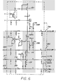
- the wake-up circuit 162 generates a signal HS1 which can be a periodic square wave signal.
- This signal as shown in Fig. 6, is input through a first resistor 284 to a logic circuit which forms an OR logic gate 286, for example.
- the similar HS 1 signal is also connected through a similar pull-up resistor 288 to the second headlight signal 282 and also to the OR gate 286.
- the output of the OR gate 286 is the signal labeled L0.
- the signal L0 is normally at a high voltage level when input to the wake-up circuit 162.
- the voltage states from the headlight signals 280 and 282, as described above, will be input to the OR gate 286 and switch the state of the L0 signal from high to low only when both signals are present, such as at each contactor 78 transition between two switch pads.
- the HS 1 signal is discontinued and the U_STALKL_ON signal is generated by the controller 160 to switch the transistor 150 Aon@ shown in Fig. 6 thereby enabling the voltages from the resistors on the circuit board 80 to be read directly through the terminals 280 and 282 to the controller 160 which will then activate the appropriate headlight commands based on the position of the actuator 32.
- the logic or gate 286 can be replaced by a NOR gate.
- the wake-up signal is a transition from a low voltage to a high voltage.
- the circuit 162 can be programmed to recognize this transition as a wake-up signal.
- the make before break function of the contactor 78 and the switch pad shown in Figs. 11 and 12 can also be implemented by providing the switch pads with generally parallel spaced edges and then forming the contactor with suitably shaped contact arms such that the contact arms will span the space between two adjacent switch pads while making contact for at least a brief instant with two adjacent switch pads.
Landscapes
- Lighting Device Outwards From Vehicle And Optical Signal (AREA)
- Input From Keyboards Or The Like (AREA)
Abstract
Description
providing a contactor bridging the ground and the switch conductive traces moveable in engagement between switch traces by movement of an actuator coupled to the contactor,
providing a resistor means coupled between the switch traces and producing a distinct analog voltage output when each switch trace is connected to ground by the contactor,
the switch traces alternatingly coupled through the resistor means to first and second outputs;
means, connected to the first and second outputs, for generating a wake-up command signal when both of the outputs are in a low voltage state.
Claims (6)
- Digital wake-up signal generation circuit which generates a digital wake-up command for waking up an electronic device from a sleep mode to an active mode in response to a detected movement of an analog output switch comprising:a printed circuit board with a ground conductive trace and at least two switch conductive traces;a contactor bridging the ground and the switch conductive traces and moveable in engagement between switch traces by movement of an actuator coupled to the contactor;resistor means coupled between the switch traces for producing a distinct analog voltage output when each switch trace is connected to ground by the contactor;the switch traces alternatingly coupled through the resistor means to first and second outputs; andmeans, connected to the first and second outputs, for generating a wake-up command signal when both of the outputs are in a low voltage state.
- Digital wake-up signal generation circuit of claim 1 wherein the wake-up command signal generating means comprises:an OR gate coupled to the first and second outputs.
- Digital wake-up signal generation circuit of claim 1 or 2
wherein:the contactor and the switch conductive traces are arranged such that the contactor contacts a next adjacent switch trace before disengaging from a proceeding switch trace. - Digital wake-up signal generation circuit of any of claims 1-3
wherein:the switch traces are one of linearly and circumferentially spaced apart. - Digital wake-up signal generation circuit of claim 4 wherein:the determining means coincides with movement of the actuator coupled to the contactor between two distinct positions.
- A method for switching an electronic device having sleep and active states from a sleep state to an active state by generating a wake-up signal from a digital wake-up signal generating device, the method comprising the steps of:providing a printed circuit board with a ground conductive trace and at least two switch conductive traces;providing a contactor bridging the ground and the switch conductive traces and moveable in engagement between switch traces by movement of an actuator coupled to the contactor;providing a resistor means coupled between the switch traces and producing a distinct analog voltage output when each switch trace is connected to ground by the contactor; andalternatingly connecting the switch traces through the resistor means to first and second outputs; anddetermining when the first and second outputs are both at a low voltage level to generate a wake-up command output signal.
Applications Claiming Priority (2)
| Application Number | Priority Date | Filing Date | Title |
|---|---|---|---|
| US748972 | 2000-12-27 | ||
| US10/748,972 US7206952B2 (en) | 2003-12-30 | 2003-12-30 | Digital wake-up signal from switch transition of two analog signals |
Publications (3)
| Publication Number | Publication Date |
|---|---|
| EP1551046A2 true EP1551046A2 (en) | 2005-07-06 |
| EP1551046A3 EP1551046A3 (en) | 2006-02-01 |
| EP1551046B1 EP1551046B1 (en) | 2016-03-30 |
Family
ID=34574781
Family Applications (1)
| Application Number | Title | Priority Date | Filing Date |
|---|---|---|---|
| EP04106378.5A Active EP1551046B1 (en) | 2003-12-30 | 2004-12-07 | Digital wake-up signal from switch transition of two analog signals |
Country Status (2)
| Country | Link |
|---|---|
| US (1) | US7206952B2 (en) |
| EP (1) | EP1551046B1 (en) |
Cited By (1)
| Publication number | Priority date | Publication date | Assignee | Title |
|---|---|---|---|---|
| WO2007009746A1 (en) * | 2005-07-21 | 2007-01-25 | Preh Gmbh | Operator's element comprising a wake-up functionality |
Families Citing this family (3)
| Publication number | Priority date | Publication date | Assignee | Title |
|---|---|---|---|---|
| WO2006100906A1 (en) * | 2005-03-18 | 2006-09-28 | Sharp Kabushiki Kaisha | Image display apparatus, image display monitor, and television receiver |
| US9839438B2 (en) | 2013-03-11 | 2017-12-12 | Biomet Manufacturing, Llc | Patient-specific glenoid guide with a reusable guide holder |
| JP6417249B2 (en) * | 2015-03-17 | 2018-10-31 | 日立オートモティブシステムズ株式会社 | Vehicle control device and vehicle control system |
Citations (8)
| Publication number | Priority date | Publication date | Assignee | Title |
|---|---|---|---|---|
| EP0458292A2 (en) * | 1990-05-25 | 1991-11-27 | ITT INDUSTRIES, INC. (a Delaware corporation) | Multifunction steering column switch |
| US5150095A (en) * | 1991-04-04 | 1992-09-22 | Appliance Control Technology, Inc. | Multi-position rotary switch with position sensor |
| US5453588A (en) * | 1992-11-06 | 1995-09-26 | Itt Corporation | Steering column stalk switch apparatus |
| EP0910105A2 (en) * | 1997-10-14 | 1999-04-21 | NEW HOLLAND ITALIA S.p.A. | Electrical switching system |
| WO1999062180A1 (en) * | 1998-05-22 | 1999-12-02 | Qualcomm Incorporated | Differentiating between input ranges in a passive keypad |
| EP1156587A2 (en) * | 2000-05-17 | 2001-11-21 | Hewlett-Packard Company | Method and apparatus for detecting switch closures |
| EP1283538A2 (en) * | 2001-08-10 | 2003-02-12 | Wacoh Corporation | Force detector |
| GB2389990A (en) * | 2002-06-18 | 2003-12-24 | Siemens Vdo Automotive Inc | Vehicle active noise cancelling system provides warning horn sounds |
Family Cites Families (5)
| Publication number | Priority date | Publication date | Assignee | Title |
|---|---|---|---|---|
| DE3615531A1 (en) | 1986-05-07 | 1987-11-12 | Swf Auto Electric Gmbh | SWITCHING ARRANGEMENT FOR AT LEAST ONE ELECTRICAL CONSUMER OF A MOTOR VEHICLE |
| US5412170A (en) | 1990-06-29 | 1995-05-02 | Itt Automotive Europe Gmbh | Electric switch with sliding bridging contact |
| US5473809A (en) | 1992-11-06 | 1995-12-12 | Itt Corporation | Method of manufacturing a steering column stalk switch apparatus |
| DE19601985A1 (en) | 1996-01-20 | 1997-07-24 | Teves Gmbh Alfred | Switch with lifting ramp |
| US6384351B1 (en) | 2000-03-23 | 2002-05-07 | Valeo Electrical Systems, Inc. | Switch apparatus for actuating a plurality of electrical circuits |
-
2003
- 2003-12-30 US US10/748,972 patent/US7206952B2/en active Active
-
2004
- 2004-12-07 EP EP04106378.5A patent/EP1551046B1/en active Active
Patent Citations (8)
| Publication number | Priority date | Publication date | Assignee | Title |
|---|---|---|---|---|
| EP0458292A2 (en) * | 1990-05-25 | 1991-11-27 | ITT INDUSTRIES, INC. (a Delaware corporation) | Multifunction steering column switch |
| US5150095A (en) * | 1991-04-04 | 1992-09-22 | Appliance Control Technology, Inc. | Multi-position rotary switch with position sensor |
| US5453588A (en) * | 1992-11-06 | 1995-09-26 | Itt Corporation | Steering column stalk switch apparatus |
| EP0910105A2 (en) * | 1997-10-14 | 1999-04-21 | NEW HOLLAND ITALIA S.p.A. | Electrical switching system |
| WO1999062180A1 (en) * | 1998-05-22 | 1999-12-02 | Qualcomm Incorporated | Differentiating between input ranges in a passive keypad |
| EP1156587A2 (en) * | 2000-05-17 | 2001-11-21 | Hewlett-Packard Company | Method and apparatus for detecting switch closures |
| EP1283538A2 (en) * | 2001-08-10 | 2003-02-12 | Wacoh Corporation | Force detector |
| GB2389990A (en) * | 2002-06-18 | 2003-12-24 | Siemens Vdo Automotive Inc | Vehicle active noise cancelling system provides warning horn sounds |
Cited By (3)
| Publication number | Priority date | Publication date | Assignee | Title |
|---|---|---|---|---|
| WO2007009746A1 (en) * | 2005-07-21 | 2007-01-25 | Preh Gmbh | Operator's element comprising a wake-up functionality |
| US7579562B2 (en) | 2005-07-21 | 2009-08-25 | Preh Gmbh | Operating element with wake-up functionality |
| DE102005055305B4 (en) * | 2005-07-21 | 2010-08-26 | Preh Gmbh | Control with wake-up functionality |
Also Published As
| Publication number | Publication date |
|---|---|
| US7206952B2 (en) | 2007-04-17 |
| EP1551046B1 (en) | 2016-03-30 |
| EP1551046A3 (en) | 2006-02-01 |
| US20050146843A1 (en) | 2005-07-07 |
Similar Documents
| Publication | Publication Date | Title |
|---|---|---|
| AU664571B2 (en) | Intelligent lamp or intelligent contact terminal for a lamp | |
| US7030326B2 (en) | Digital wake-up signal from analog signal transition | |
| US6570105B1 (en) | Retractable rotary switch cell | |
| EP1551046B1 (en) | Digital wake-up signal from switch transition of two analog signals | |
| EP0980083A2 (en) | Variable resistance switch | |
| US20060119570A1 (en) | Switch and method of combining multiple switch functions into a single switch | |
| KR19990083237A (en) | Electronic blinker | |
| US6700084B2 (en) | Switch structure with electrical device | |
| AU688947B2 (en) | Manually actuatable integrated control module and method of making same | |
| JP5519658B2 (en) | Switch assembly at the top of an automotive steering column and corresponding control assembly and control method | |
| US6846997B2 (en) | Contact structure of combination switch | |
| EP0910105B1 (en) | Electrical switching system | |
| US20020139648A1 (en) | Multifunctional lever stalk | |
| RU2339523C1 (en) | Control module for vehicle lighting devices | |
| JPH09185929A (en) | Lighting switch device containing daytime running light control circuit | |
| KR101526406B1 (en) | In-vehicle wiper switching apparatus | |
| CA2297884A1 (en) | Daytime running light circuit | |
| EP0774380B1 (en) | Improved-wiring device for controlling the emergency lights in motor vehicles | |
| US7057121B2 (en) | Low-current starter switch for vehicles and starter gear comprising said switch | |
| KR100391725B1 (en) | Apparatus of head lamp for vehicle | |
| JP2597481Y2 (en) | In-vehicle switch device | |
| US3240890A (en) | Direction signaling and auxiliary switching apparatus | |
| JPH0212112Y2 (en) | ||
| JPS6361659A (en) | Head lamp circuit in lighting device for vehicle | |
| JPH1170834A (en) | Hazard switch device for automobile |
Legal Events
| Date | Code | Title | Description |
|---|---|---|---|
| PUAI | Public reference made under article 153(3) epc to a published international application that has entered the european phase |
Free format text: ORIGINAL CODE: 0009012 |
|
| AK | Designated contracting states |
Kind code of ref document: A2 Designated state(s): AT BE BG CH CY CZ DE DK EE ES FI FR GB GR HU IE IS IT LI LT LU MC NL PL PT RO SE SI SK TR |
|
| AX | Request for extension of the european patent |
Extension state: AL BA HR LV MK YU |
|
| PUAL | Search report despatched |
Free format text: ORIGINAL CODE: 0009013 |
|
| AK | Designated contracting states |
Kind code of ref document: A3 Designated state(s): AT BE BG CH CY CZ DE DK EE ES FI FR GB GR HU IE IS IT LI LT LU MC NL PL PT RO SE SI SK TR |
|
| AX | Request for extension of the european patent |
Extension state: AL BA HR LV MK YU |
|
| 17P | Request for examination filed |
Effective date: 20060627 |
|
| AKX | Designation fees paid |
Designated state(s): AT BE BG CH CY CZ DE DK EE ES FI FR GB GR HU IE IS IT LI LT LU MC NL PL PT RO SE SI SK TR |
|
| 17Q | First examination report despatched |
Effective date: 20120404 |
|
| GRAP | Despatch of communication of intention to grant a patent |
Free format text: ORIGINAL CODE: EPIDOSNIGR1 |
|
| INTG | Intention to grant announced |
Effective date: 20150930 |
|
| GRAS | Grant fee paid |
Free format text: ORIGINAL CODE: EPIDOSNIGR3 |
|
| GRAA | (expected) grant |
Free format text: ORIGINAL CODE: 0009210 |
|
| AK | Designated contracting states |
Kind code of ref document: B1 Designated state(s): AT BE BG CH CY CZ DE DK EE ES FI FR GB GR HU IE IS IT LI LT LU MC NL PL PT RO SE SI SK TR |
|
| REG | Reference to a national code |
Ref country code: GB Ref legal event code: FG4D |
|
| REG | Reference to a national code |
Ref country code: CH Ref legal event code: EP |
|
| REG | Reference to a national code |
Ref country code: AT Ref legal event code: REF Ref document number: 786168 Country of ref document: AT Kind code of ref document: T Effective date: 20160415 |
|
| REG | Reference to a national code |
Ref country code: IE Ref legal event code: FG4D |
|
| REG | Reference to a national code |
Ref country code: DE Ref legal event code: R096 Ref document number: 602004048908 Country of ref document: DE |
|
| REG | Reference to a national code |
Ref country code: LT Ref legal event code: MG4D |
|
| PG25 | Lapsed in a contracting state [announced via postgrant information from national office to epo] |
Ref country code: FI Free format text: LAPSE BECAUSE OF FAILURE TO SUBMIT A TRANSLATION OF THE DESCRIPTION OR TO PAY THE FEE WITHIN THE PRESCRIBED TIME-LIMIT Effective date: 20160330 Ref country code: GR Free format text: LAPSE BECAUSE OF FAILURE TO SUBMIT A TRANSLATION OF THE DESCRIPTION OR TO PAY THE FEE WITHIN THE PRESCRIBED TIME-LIMIT Effective date: 20160701 |
|
| REG | Reference to a national code |
Ref country code: NL Ref legal event code: MP Effective date: 20160330 |
|
| REG | Reference to a national code |
Ref country code: AT Ref legal event code: MK05 Ref document number: 786168 Country of ref document: AT Kind code of ref document: T Effective date: 20160330 |
|
| PG25 | Lapsed in a contracting state [announced via postgrant information from national office to epo] |
Ref country code: SE Free format text: LAPSE BECAUSE OF FAILURE TO SUBMIT A TRANSLATION OF THE DESCRIPTION OR TO PAY THE FEE WITHIN THE PRESCRIBED TIME-LIMIT Effective date: 20160330 Ref country code: LT Free format text: LAPSE BECAUSE OF FAILURE TO SUBMIT A TRANSLATION OF THE DESCRIPTION OR TO PAY THE FEE WITHIN THE PRESCRIBED TIME-LIMIT Effective date: 20160330 |
|
| PG25 | Lapsed in a contracting state [announced via postgrant information from national office to epo] |
Ref country code: NL Free format text: LAPSE BECAUSE OF FAILURE TO SUBMIT A TRANSLATION OF THE DESCRIPTION OR TO PAY THE FEE WITHIN THE PRESCRIBED TIME-LIMIT Effective date: 20160330 |
|
| PG25 | Lapsed in a contracting state [announced via postgrant information from national office to epo] |
Ref country code: PL Free format text: LAPSE BECAUSE OF FAILURE TO SUBMIT A TRANSLATION OF THE DESCRIPTION OR TO PAY THE FEE WITHIN THE PRESCRIBED TIME-LIMIT Effective date: 20160330 Ref country code: EE Free format text: LAPSE BECAUSE OF FAILURE TO SUBMIT A TRANSLATION OF THE DESCRIPTION OR TO PAY THE FEE WITHIN THE PRESCRIBED TIME-LIMIT Effective date: 20160330 Ref country code: IS Free format text: LAPSE BECAUSE OF FAILURE TO SUBMIT A TRANSLATION OF THE DESCRIPTION OR TO PAY THE FEE WITHIN THE PRESCRIBED TIME-LIMIT Effective date: 20160730 |
|
| PG25 | Lapsed in a contracting state [announced via postgrant information from national office to epo] |
Ref country code: SK Free format text: LAPSE BECAUSE OF FAILURE TO SUBMIT A TRANSLATION OF THE DESCRIPTION OR TO PAY THE FEE WITHIN THE PRESCRIBED TIME-LIMIT Effective date: 20160330 Ref country code: ES Free format text: LAPSE BECAUSE OF FAILURE TO SUBMIT A TRANSLATION OF THE DESCRIPTION OR TO PAY THE FEE WITHIN THE PRESCRIBED TIME-LIMIT Effective date: 20160330 Ref country code: RO Free format text: LAPSE BECAUSE OF FAILURE TO SUBMIT A TRANSLATION OF THE DESCRIPTION OR TO PAY THE FEE WITHIN THE PRESCRIBED TIME-LIMIT Effective date: 20160330 Ref country code: PT Free format text: LAPSE BECAUSE OF FAILURE TO SUBMIT A TRANSLATION OF THE DESCRIPTION OR TO PAY THE FEE WITHIN THE PRESCRIBED TIME-LIMIT Effective date: 20160801 Ref country code: CZ Free format text: LAPSE BECAUSE OF FAILURE TO SUBMIT A TRANSLATION OF THE DESCRIPTION OR TO PAY THE FEE WITHIN THE PRESCRIBED TIME-LIMIT Effective date: 20160330 Ref country code: AT Free format text: LAPSE BECAUSE OF FAILURE TO SUBMIT A TRANSLATION OF THE DESCRIPTION OR TO PAY THE FEE WITHIN THE PRESCRIBED TIME-LIMIT Effective date: 20160330 |
|
| REG | Reference to a national code |
Ref country code: FR Ref legal event code: PLFP Year of fee payment: 13 |
|
| PG25 | Lapsed in a contracting state [announced via postgrant information from national office to epo] |
Ref country code: IT Free format text: LAPSE BECAUSE OF FAILURE TO SUBMIT A TRANSLATION OF THE DESCRIPTION OR TO PAY THE FEE WITHIN THE PRESCRIBED TIME-LIMIT Effective date: 20160330 Ref country code: BE Free format text: LAPSE BECAUSE OF FAILURE TO SUBMIT A TRANSLATION OF THE DESCRIPTION OR TO PAY THE FEE WITHIN THE PRESCRIBED TIME-LIMIT Effective date: 20160330 |
|
| REG | Reference to a national code |
Ref country code: DE Ref legal event code: R097 Ref document number: 602004048908 Country of ref document: DE |
|
| PG25 | Lapsed in a contracting state [announced via postgrant information from national office to epo] |
Ref country code: DK Free format text: LAPSE BECAUSE OF FAILURE TO SUBMIT A TRANSLATION OF THE DESCRIPTION OR TO PAY THE FEE WITHIN THE PRESCRIBED TIME-LIMIT Effective date: 20160330 |
|
| PLBE | No opposition filed within time limit |
Free format text: ORIGINAL CODE: 0009261 |
|
| STAA | Information on the status of an ep patent application or granted ep patent |
Free format text: STATUS: NO OPPOSITION FILED WITHIN TIME LIMIT |
|
| 26N | No opposition filed |
Effective date: 20170103 |
|
| PG25 | Lapsed in a contracting state [announced via postgrant information from national office to epo] |
Ref country code: SI Free format text: LAPSE BECAUSE OF FAILURE TO SUBMIT A TRANSLATION OF THE DESCRIPTION OR TO PAY THE FEE WITHIN THE PRESCRIBED TIME-LIMIT Effective date: 20160330 |
|
| REG | Reference to a national code |
Ref country code: CH Ref legal event code: PL |
|
| GBPC | Gb: european patent ceased through non-payment of renewal fee |
Effective date: 20161207 |
|
| PG25 | Lapsed in a contracting state [announced via postgrant information from national office to epo] |
Ref country code: MC Free format text: LAPSE BECAUSE OF FAILURE TO SUBMIT A TRANSLATION OF THE DESCRIPTION OR TO PAY THE FEE WITHIN THE PRESCRIBED TIME-LIMIT Effective date: 20160330 |
|
| REG | Reference to a national code |
Ref country code: IE Ref legal event code: MM4A |
|
| PG25 | Lapsed in a contracting state [announced via postgrant information from national office to epo] |
Ref country code: LI Free format text: LAPSE BECAUSE OF NON-PAYMENT OF DUE FEES Effective date: 20161231 Ref country code: LU Free format text: LAPSE BECAUSE OF NON-PAYMENT OF DUE FEES Effective date: 20161207 Ref country code: CH Free format text: LAPSE BECAUSE OF NON-PAYMENT OF DUE FEES Effective date: 20161231 |
|
| PG25 | Lapsed in a contracting state [announced via postgrant information from national office to epo] |
Ref country code: GB Free format text: LAPSE BECAUSE OF NON-PAYMENT OF DUE FEES Effective date: 20161207 Ref country code: IE Free format text: LAPSE BECAUSE OF NON-PAYMENT OF DUE FEES Effective date: 20161207 |
|
| REG | Reference to a national code |
Ref country code: FR Ref legal event code: PLFP Year of fee payment: 14 |
|
| PG25 | Lapsed in a contracting state [announced via postgrant information from national office to epo] |
Ref country code: HU Free format text: LAPSE BECAUSE OF FAILURE TO SUBMIT A TRANSLATION OF THE DESCRIPTION OR TO PAY THE FEE WITHIN THE PRESCRIBED TIME-LIMIT; INVALID AB INITIO Effective date: 20041207 Ref country code: CY Free format text: LAPSE BECAUSE OF FAILURE TO SUBMIT A TRANSLATION OF THE DESCRIPTION OR TO PAY THE FEE WITHIN THE PRESCRIBED TIME-LIMIT Effective date: 20160330 |
|
| PG25 | Lapsed in a contracting state [announced via postgrant information from national office to epo] |
Ref country code: TR Free format text: LAPSE BECAUSE OF FAILURE TO SUBMIT A TRANSLATION OF THE DESCRIPTION OR TO PAY THE FEE WITHIN THE PRESCRIBED TIME-LIMIT Effective date: 20160330 |
|
| PG25 | Lapsed in a contracting state [announced via postgrant information from national office to epo] |
Ref country code: BG Free format text: LAPSE BECAUSE OF FAILURE TO SUBMIT A TRANSLATION OF THE DESCRIPTION OR TO PAY THE FEE WITHIN THE PRESCRIBED TIME-LIMIT Effective date: 20160330 |
|
| P01 | Opt-out of the competence of the unified patent court (upc) registered |
Effective date: 20230528 |
|
| PGFP | Annual fee paid to national office [announced via postgrant information from national office to epo] |
Ref country code: FR Payment date: 20231220 Year of fee payment: 20 Ref country code: DE Payment date: 20231208 Year of fee payment: 20 |