EP1550904A1 - Recording device and recorder - Google Patents
Recording device and recorder Download PDFInfo
- Publication number
- EP1550904A1 EP1550904A1 EP03701885A EP03701885A EP1550904A1 EP 1550904 A1 EP1550904 A1 EP 1550904A1 EP 03701885 A EP03701885 A EP 03701885A EP 03701885 A EP03701885 A EP 03701885A EP 1550904 A1 EP1550904 A1 EP 1550904A1
- Authority
- EP
- European Patent Office
- Prior art keywords
- recording device
- recorder
- electrodes
- light source
- light
- Prior art date
- Legal status (The legal status is an assumption and is not a legal conclusion. Google has not performed a legal analysis and makes no representation as to the accuracy of the status listed.)
- Withdrawn
Links
Images




Classifications
-
- G—PHYSICS
- G02—OPTICS
- G02F—OPTICAL DEVICES OR ARRANGEMENTS FOR THE CONTROL OF LIGHT BY MODIFICATION OF THE OPTICAL PROPERTIES OF THE MEDIA OF THE ELEMENTS INVOLVED THEREIN; NON-LINEAR OPTICS; FREQUENCY-CHANGING OF LIGHT; OPTICAL LOGIC ELEMENTS; OPTICAL ANALOGUE/DIGITAL CONVERTERS
- G02F1/00—Devices or arrangements for the control of the intensity, colour, phase, polarisation or direction of light arriving from an independent light source, e.g. switching, gating or modulating; Non-linear optics
- G02F1/01—Devices or arrangements for the control of the intensity, colour, phase, polarisation or direction of light arriving from an independent light source, e.g. switching, gating or modulating; Non-linear optics for the control of the intensity, phase, polarisation or colour
- G02F1/13—Devices or arrangements for the control of the intensity, colour, phase, polarisation or direction of light arriving from an independent light source, e.g. switching, gating or modulating; Non-linear optics for the control of the intensity, phase, polarisation or colour based on liquid crystals, e.g. single liquid crystal display cells
- G02F1/133—Constructional arrangements; Operation of liquid crystal cells; Circuit arrangements
- G02F1/135—Liquid crystal cells structurally associated with a photoconducting or a ferro-electric layer, the properties of which can be optically or electrically varied
-
- G—PHYSICS
- G02—OPTICS
- G02F—OPTICAL DEVICES OR ARRANGEMENTS FOR THE CONTROL OF LIGHT BY MODIFICATION OF THE OPTICAL PROPERTIES OF THE MEDIA OF THE ELEMENTS INVOLVED THEREIN; NON-LINEAR OPTICS; FREQUENCY-CHANGING OF LIGHT; OPTICAL LOGIC ELEMENTS; OPTICAL ANALOGUE/DIGITAL CONVERTERS
- G02F1/00—Devices or arrangements for the control of the intensity, colour, phase, polarisation or direction of light arriving from an independent light source, e.g. switching, gating or modulating; Non-linear optics
- G02F1/01—Devices or arrangements for the control of the intensity, colour, phase, polarisation or direction of light arriving from an independent light source, e.g. switching, gating or modulating; Non-linear optics for the control of the intensity, phase, polarisation or colour
- G02F1/13—Devices or arrangements for the control of the intensity, colour, phase, polarisation or direction of light arriving from an independent light source, e.g. switching, gating or modulating; Non-linear optics for the control of the intensity, phase, polarisation or colour based on liquid crystals, e.g. single liquid crystal display cells
- G02F1/133—Constructional arrangements; Operation of liquid crystal cells; Circuit arrangements
- G02F1/1333—Constructional arrangements; Manufacturing methods
- G02F1/1343—Electrodes
- G02F1/134309—Electrodes characterised by their geometrical arrangement
-
- G—PHYSICS
- G02—OPTICS
- G02F—OPTICAL DEVICES OR ARRANGEMENTS FOR THE CONTROL OF LIGHT BY MODIFICATION OF THE OPTICAL PROPERTIES OF THE MEDIA OF THE ELEMENTS INVOLVED THEREIN; NON-LINEAR OPTICS; FREQUENCY-CHANGING OF LIGHT; OPTICAL LOGIC ELEMENTS; OPTICAL ANALOGUE/DIGITAL CONVERTERS
- G02F1/00—Devices or arrangements for the control of the intensity, colour, phase, polarisation or direction of light arriving from an independent light source, e.g. switching, gating or modulating; Non-linear optics
- G02F1/01—Devices or arrangements for the control of the intensity, colour, phase, polarisation or direction of light arriving from an independent light source, e.g. switching, gating or modulating; Non-linear optics for the control of the intensity, phase, polarisation or colour
- G02F1/13—Devices or arrangements for the control of the intensity, colour, phase, polarisation or direction of light arriving from an independent light source, e.g. switching, gating or modulating; Non-linear optics for the control of the intensity, phase, polarisation or colour based on liquid crystals, e.g. single liquid crystal display cells
- G02F1/133—Constructional arrangements; Operation of liquid crystal cells; Circuit arrangements
- G02F1/135—Liquid crystal cells structurally associated with a photoconducting or a ferro-electric layer, the properties of which can be optically or electrically varied
- G02F1/1357—Electrode structure
-
- G—PHYSICS
- G02—OPTICS
- G02F—OPTICAL DEVICES OR ARRANGEMENTS FOR THE CONTROL OF LIGHT BY MODIFICATION OF THE OPTICAL PROPERTIES OF THE MEDIA OF THE ELEMENTS INVOLVED THEREIN; NON-LINEAR OPTICS; FREQUENCY-CHANGING OF LIGHT; OPTICAL LOGIC ELEMENTS; OPTICAL ANALOGUE/DIGITAL CONVERTERS
- G02F1/00—Devices or arrangements for the control of the intensity, colour, phase, polarisation or direction of light arriving from an independent light source, e.g. switching, gating or modulating; Non-linear optics
- G02F1/01—Devices or arrangements for the control of the intensity, colour, phase, polarisation or direction of light arriving from an independent light source, e.g. switching, gating or modulating; Non-linear optics for the control of the intensity, phase, polarisation or colour
- G02F1/13—Devices or arrangements for the control of the intensity, colour, phase, polarisation or direction of light arriving from an independent light source, e.g. switching, gating or modulating; Non-linear optics for the control of the intensity, phase, polarisation or colour based on liquid crystals, e.g. single liquid crystal display cells
- G02F1/137—Devices or arrangements for the control of the intensity, colour, phase, polarisation or direction of light arriving from an independent light source, e.g. switching, gating or modulating; Non-linear optics for the control of the intensity, phase, polarisation or colour based on liquid crystals, e.g. single liquid crystal display cells characterised by the electro-optical or magneto-optical effect, e.g. field-induced phase transition, orientation effect, guest-host interaction or dynamic scattering
- G02F1/13718—Devices or arrangements for the control of the intensity, colour, phase, polarisation or direction of light arriving from an independent light source, e.g. switching, gating or modulating; Non-linear optics for the control of the intensity, phase, polarisation or colour based on liquid crystals, e.g. single liquid crystal display cells characterised by the electro-optical or magneto-optical effect, e.g. field-induced phase transition, orientation effect, guest-host interaction or dynamic scattering based on a change of the texture state of a cholesteric liquid crystal
-
- G—PHYSICS
- G09—EDUCATION; CRYPTOGRAPHY; DISPLAY; ADVERTISING; SEALS
- G09G—ARRANGEMENTS OR CIRCUITS FOR CONTROL OF INDICATING DEVICES USING STATIC MEANS TO PRESENT VARIABLE INFORMATION
- G09G3/00—Control arrangements or circuits, of interest only in connection with visual indicators other than cathode-ray tubes
- G09G3/001—Control arrangements or circuits, of interest only in connection with visual indicators other than cathode-ray tubes using specific devices not provided for in groups G09G3/02 - G09G3/36, e.g. using an intermediate record carrier such as a film slide; Projection systems; Display of non-alphanumerical information, solely or in combination with alphanumerical information, e.g. digital display on projected diapositive as background
Definitions
- the present invention relates to a recording device suitable for use as, for example, electronic paper and a recorder.
- information input means including a scanner and a digital camera, display devices including a monitor, and information output means including a printer have been used diversely along with the development of electronic information equipment.
- Information can be read directly from a display device such as a monitor.
- the display device such as a monitor is generally of an emissive type and therefore fatigues viewer's eyes.
- the resolution offered by the display device is not very high, direct reading of a document or still image from the display device such as a monitor may not be desired. Therefore, information recorded in electronic information equipment is often printed onto paper in order to read the information on the paper.
- a printer when a printer is used to produce a hardcopy of a document or an image, if the printer is an ink-jet printer, not only paper but also inks of primary colors such as cyan, magenta, and yellow, or of more colors are consumed. If the printer is a laser printer or an LED printer, toners of many colors are consumed. The use of the consumables required for printout onto paper imposes a large load on an environment.
- a rewritable (re-recordable) type recording device called electronic paper has been proposed and under development.
- an electrophoretic recording device, a twisted-ball type recording device, and a selective reflection type recording device employing a cholesteric liquid crystal have been proposed as reflective recording devices that have the capability of a memory.
- the electrophoretic recording device has been disclosed in, for example, the proceedings of the IEEE (Vol. 61, No. 7, July 1973) or Nature (Vol. 394, No. 16, July 1988).
- the twist ball type recording device has been disclosed in, for example, the proceedings of the SID (Vol. 18, 3rd and 4th Quarters, 1977, p.289).
- Japanese Translation of PCT International Application No. 6-507505 has disclosed a liquid crystal cell having chiral nematic liquid crystalline molecules dispersed in the network of a polymer.
- One form of the liquid crystal cell allows a liquid crystal to become reflective or transmissive (diffusible), and the liquid crystal is stable with a zero voltage in both the reflective and transmissive states.
- Japanese Unexamined Patent Application Publication No. 9-105900 has disclosed an optically writable projection liquid crystal display device including a spatial modulator that has a photoconductive layer and a liquid crystal layer. Light is irradiated to the photoconductive layer, whereby information is written in the liquid crystal layer.
- a recording device composed of a photoconductive layer and a cholesteric liquid crystal has been disclosed in "Reflective Display with Photoconductive Layer and Bistable Reflective Cholesteric Mixture” (SID 96 Applications Digest, p.59).
- the recording device is used as a screen capture that is mounted on the screen of a personal computer in order to copy a screen image on the personal computer. Since the recording device preserves the copied screen image as if to be a memory, no power is consumed. Recording and deletion are achieved instantaneously.
- the electronic paper obviates the necessity of a printer and paper, and is therefore inexpensive. Moreover, the electronic paper imposes no load on an environment. However, the recording devices that write information using light are susceptible to noise caused by extraneous light and likely to produce unclear images.
- An object of the present invention is to provide an optically writable recording device that is inexpensive and highly reliable and a recorder for recording information in the recording device.
- a recording device in accordance with the present invention comprises a display, a photoconductor superposed on the display, and a pair of electrodes disposed on the display and photoconductor respectively. At least one of the pair of electrodes is divided into a plurality of sub-electrodes.
- At least one of the pair of electrodes is divided in to a plurality of sub-electrodes. While a voltage is applied to each of the sub-electrodes, information is written using light. Even if extraneous light falls on part of the recording device corresponding to the sub-electrodes to which no voltage is applied, no information is written. Consequently, a sharp image devoid of noise is produced. According to the present invention, there is provided an optically writable recording device that is inexpensive and highly reliable.
- an electrode When an electrode is divided in to a plurality of sub-electrodes, a border between adjoining sub-electrodes is visualized as a streaky image on a display surface.
- the opposite ends of adjoining sub-electrodes are curved as randomly as possible so that the streak will be unobtrusive.
- an electric field which is regarded as a vector, induced between the pair of electrodes may be made oblique to the surface of a substrate.
- a recorder in accordance with the present invention records information in a recoding device comprising a display, a photoconductor superposed on the display, and a pair of electrodes disposed on the display and photoconductor respectively.
- the recorder comprises feed members via which a voltage is applied to the pair of electrodes included in the recording device, a first light source required for writing of information in the recording device, and a second light source required for resetting a record in the recording device.
- the first light source generates light that flickers according to a signal and with which information is recorded in the recording device.
- the second light source is used to initialize the recording device. Consequently, the one recorder can smoothly perform both recording and reset.
- the first light source is realized with an LED array having LEDs disposed linearly or a laser that flickers light linearly.
- the second light source is realized with any of a light source composed of an LED that generates light on a planar basis or in a wide range and a light guide, or a light source compose of an electroluminescent (EL) lamp or a fluorescent lamp and a light guide.
- the first light source and/or second light source have a light adjustment ability to adjust the intensity of light.
- the recorder in accordance with the present invention including the LED array and planar light source does not, unlike a printer, include a mechanism for fusing ink or toner onto paper but records information in the recording device merely by controlling light and electricity. Various members included in the printer are unnecessary. A low cost and a drastically compact design can be realized.
- the recording device Since the recording device is rewritable (re-recordable), the recording device will not, unlike conventional devices, consume a large amount of paper.
- the recording device has the capability of a memory to preserve a record even with no power fed. Therefore, the power consumption is small and a load on an environment is drastically reduced.
- a type of recording device employing a cholesteric liquid crystal has potentials for greater brightness, a higher contrast, and a higher resolution.
- FIG. 1 is a sectional view showing a recording device in accordance with an embodiment of the present invention.
- a recording device 10 comprises transparent substrates 12 and 14, transparent electrodes 16 and 18 formed on the substrates 12 and 14 respectively, a display layer 20, and a photoconductive layer 24 superposed on the display layer 20 with a partition layer 22 between them.
- the electrodes 16 and 18 are disposed on the display layer 20 and photoconductive layer 24 respectively.
- the display layer 20 and photoconductive layer 24 are sealed with a sealant 26.
- an optical absorption layer 28 is sandwiched between the photoconductive layer 24 and electrode 16.
- the partition layer 22 prevents mixture of the display layer 20 and photoconductive layer 24.
- the partition layer 22 may be realized with an optical absorption layer.
- the partition layer 22 is preferably made of a material exhibiting as high a permittivity as possible in order to prevent a driving voltage to rise, but is not limited to any specific material.
- FIG. 2 schematically shows a recorder in accordance with the embodiment of the present invention.
- a recorder 30 records information in the recording device 10 shown in Fig. 1.
- the recorder 30 comprises a casing 32 in which the recording device 10 is supported or disposed, feed members 34, 36, and 37 via which a voltage is applied to the pair of electrodes 16 and 18 of the recording device 10, a first light source 38 for writing information in the recording device 10, and a second light source 40 for resetting a record produced in the recording device 10.
- the feed members 34, 36, and 37 are connected to a power supply that is not shown.
- Figure 3 is a plan view showing the recording device 10 in which information is recorded.
- the information is recorded in the form of, for example, characters or an image.
- Figure 4 is a plan view showing the electrode 18 included in the recording device 10.
- the electrode 18 is divided into a plurality of sub-electrodes 18A.
- the sub-electrodes 18A are shaped like stripes.
- the width of the sub-electrodes 18A is equal to or larger than 1 cm.
- a microscopic gap 18B is interposed between two adjoining sub-electrodes 18A.
- the gap 18B is equal to or smaller than 50 ⁇ m. Since the gap 18B is as small as 50 ⁇ m or less, the gap 18B will not be discerned as a streak in a screen image.
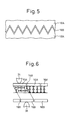
- Figure 5 is a plan view showing the electrode 18 included in a variant of the recording device 10.
- the electrode 18 is divided into a plurality of sub-electrodes 18A.
- the opposite ends of the sub-electrodes 18 are curved (or zigzagged).
- the opposite ends of the sub-electrodes 18A (that is, the gap 18B) are shaped as randomly as possible, whereby the gap 18B is prevented from being discerned as a streak in a screen image.
- Figure 6 is a plan view showing the electrodes 16 and 18 included in a variant of the recording device 10.
- the direction of an electric field that is regarded as a vector and induced between the pair of electrodes 16 and 18 is oblique to the surfaces of the substrates.
- the electrode 16 is divided into a plurality of sub-electrodes 16A, and the electrode 18 is divided in to a plurality of sub-electrodes 18A.
- the sub-electrodes 16A and sub-electrodes 18A are dislocated relative to each other, and the direction of the electric field induced between each of the sub-electrodes 16 and each of the sub-electrodes 18 is oblique to the surfaces of the substrates.
- Information can be printed on portions of the display layer adjoining the gaps 16B and gaps 18B, though it is imperfect.
- the gaps 16B and gaps 18B are visualized unobtrusively in an image. In the case of Fig. 5, light is randomly dispersed so that the gap 18B will be visualized unobtrusively. In the case of Fig. 6, light is dimmed so that the gaps 16B and 18B will be visualized unobtrusively.
- the display layer 20 shown in Fig. 1 is made of a cholesteric liquid crystal.
- Figures 7A and 7B show the aligned state of cholesteric liquid crystalline molecules.
- the cholesteric liquid crystal enters either a planar state shown in Fig. 7A or a focal conic state shown in Fig. 7B. In either the planar state or focal conic state, the cholesteric liquid crystal remains stable even with no electric field induced.
- the planar state since incident light is reflected from the liquid crystal, human eyes can see the reflected light.
- the focal conic state incident light passes through the liquid crystal. Since the light absorption layer 28 is included separately from the liquid crystal layer, black can be displayed in the focal conic state.
- n denotes an average refractive index of a liquid crystal
- p denotes the helical pitch
- a reflective band ⁇ increases proportionally to the anisotropy ⁇ n of a refractive index of the liquid crystal.
- Figures 8A, 8B and 8C show the characteristic of a cholesteric liquid crystal relative to a voltage that is applied in order to drive the cholesteric liquid crystal (the relationship of the voltage to a time).
- a strong electric field is induced in the liquid crystal, the helical structure of liquid crystalline molecules is completely collapsed, and all the molecules enter a homeotropic state, that is, are aligned with the direction of the electric field.
- H denotes the homeotropic state.
- the planar state and focal conic state coexist. This enables halftone display.
- the cholesteric liquid crystal is bistable. This phenomenon is used to display information.
- Figure 9 shows the characteristic of the reflectance of the cholesteric liquid crystal (the relationship of the reflectance to a voltage).
- Figure 9 graphically shows the response time which the cholesteric liquid crystal needs to respond to a voltage and which has been described in conjunction with Figs. 8A, 8B and 8C.
- the initial state of the cholesteric liquid crystal is the planar state (indicated with the left part of Fig. 9, that is, related to a high reflectance)
- the pulsating voltage falls within a range of driving voltages which bring the cholesteric liquid crystal to the focal conic state (related to a low reflectance in Fig. 9).
- the pulsating voltage is further raised, it falls within a range of driving voltages which bring the cholesteric liquid crystal to the planar state (indicated with the right part of Fig. 9 and related to high voltages).
- the pulsating voltage When the initial state of the cholesteric liquid crystal is the focal conic state (indicated with the left part of Fig. 9 and related to a low reflectance), as the pulsating voltage is raised, the pulsating voltage gradually falls within a range of driving voltages which bring the cholesteric liquid crystal to the planar state.
- Figure 10 is an explanatory diagram concerning the operation of the recording device 10 shown in Fig. 1.
- the electrodes 16 and 18 are borne by the substrates 12 and 14 respectively, and connected to a power supply 42 via feed members (contacts).
- the substrates 12 and 14 may be made of a glass.
- the substrates 12 and 14 are made of a flexible material such as a film so that the recording device can be folded like paper and then carried with a user or can be curved for recording.
- the photoconductive layer 24 may be made of an inorganic material such as an amorphous silicon or an organic material.
- a flexible and organic photoconductor would be more suitable for the recording device 10 in accordance with the present invention.
- the organic photoconductor is abbreviated to OPC and is widely used for printers or the like.
- the photoconductive layer 24 is realized with the OPC, or more particularly, a functionally separated organic OPC composed of two functional films, that is, a charge generation layer 24A and a charge transport layer 24B.
- the functionally separated OPC has many merits including the merit of excellent reformability.
- the photoconductive layer 24 is not limited to the functionally separated OPC but may be made of a monolayer OPC that has only one layer and generates and transports charge.
- the monolayer OPC has been employed for more years than the functional separated OPC has, and is said to exhibit poor reformability.
- the monolayer OPC can employed without concern.
- Figures 11 and 12 show the display characteristic (reflectance) of the recording device 10 having the combination of the cholesteric liquid crystal layer and photoconductive layer.
- Figures 11 and 12 are analogous to Fig. 9.
- Figure 11 shows the display characteristic, which is exhibited during a transition from the planar state to the focal conic state when light is irradiated, in comparison with the one exhibited when no light is irradiated.
- a curve A indicates the display characteristic exhibited when light is irradiated
- a curve B indicates the display characteristic exhibited when no light is irradiated.
- a threshold Vtf' causing the liquid crystal layer to make a transition to the focal conic state and a voltage Vfc' causing the liquid crystal layer to fully enter the focal conic state are higher than those required when light is irradiated.
- the voltage Vfc causing the liquid crystal to enter the focal conic state when light is irradiated is lower than the threshold Vtf' causing the liquid crystal to make a transition to the focal conic state when no light is irradiated.
- the application of the voltage Vfc causes the portion of the liquid crystal, to which light is irradiated, to make a transition to the focal conic state, but causes the portion thereof, to which no light is irradiated, to remain in the planar state.
- Figure 12 shows the display characteristic, which is exhibited during a transition from the focal conic state to the planar state when light is irradiated, in comparison with the one exhibited when no light is irradiated.
- a curve C indicates the display characteristic exhibited with light irradiated
- a curve D indicates the display characteristic exhibited with no light irradiated.
- Figure 13 shows the connection of the recorder 30 shown in Fig. 2 to an information processing terminal 44.
- the recorder 30 receives information from a personal computer or any other information processing terminal 44, and writes the information in the recording device 10.
- the recorder 30 is controlled by the personal computer or any other information processing terminal 44.
- a first light source 38 for recording is swept while sequentially irradiating light to the recording device 10 in a lateral direction of the recording device 10 using an LED array or a semiconductor laser. Furthermore, the first light source 38 is moved in a longitudinal direction of the recording device 10 as indicated with an arrow in order to scan the recording device 10. Otherwise, the recording device 10 may be moved with the first light source 38 held stationary. Using the LED array, the first light source 38 is realized inexpensively and simply.
- a second light source 40 is a light source for reset.
- the second light source 40 is realized using an LED, an organic electroluminescent lamp, or a fluorescent lamp that enables uniform exposure. Moreover, any of these members may be used in combination with a light guide plate.
- the second light source 40 is lit over a wide range in order to irradiate light to the photoconductive layer 24.
- a pulsating signal is applied to the electrodes 16 and 18 of the recording device 10 via the feed members 34 and 37. Consequently, the liquid crystal is entirely initialized into the planar state.
- the reason why light is irradiated to the photoconductive layer 24 for reset is that when light is irradiated to the photoconductive layer 24, the resistance given by the photoconductive layer 24 decreases and an apparent voltage to be applied to the liquid crystal falls.
- the liquid crystal can be initialized into the planar state with application of a lower voltage. Even if the second light source 40 is not included, as long as a high voltage is applied, the liquid crystal can be driven to the planar state. However, especially when the recording device is large in size, after a voltage is applied, a large current flows instantaneously. This is critical in terms of safety.
- the liquid crystal when the liquid crystal is reset by applying a relatively low voltage thereto with light irradiated, it is more advantageous in terms of safety.
- irradiation of light to the photoconductive layer 24 for a long period of time may invite fatigue and deterioration of the photoconductive layer 24. Therefore, the irradiation of light from the planar light source should be performed basically solely for the purpose of reset and completed for as short a period as possible.
- the first light source 38 (LED array) to be used for recording is generally characterized by a small focal depth and tends to become out of focus. Therefore, preferably, the focal length of the first light source is made adjustable. The focus of the first light source may be adjusted manually or automatically.
- the first light source (LED array) 38 or the recording device 10 itself is swept in a sub-scanning direction.
- the recorder is designed to be of either of two types described below.
- Figure 14 is a perspective view showing an example of a flatbed recorder.
- the recorder 30 has the features that information recorded in the recording device 10 can be discerned in real time and the recorder is thin.
- the thin casing 32 that looks like a tablet has a support base on which the recording device 10 is placed.
- the first light source 38 realized with an LED array is swept for recording.
- Figure 15 shows the first light source 38 and an interceptive member 46 included in the flatbed recorder 30 shown in Fig. 14.
- the first light source 38 is located below the recording device 10, and light is irradiated to the photoconductive layer 24 located on the back of the recording device 10.
- the interceptive member 46 is located above the recording device 10 in order to prevent extraneous light from falling on the top of the recording device 10.
- the interceptive member 46 has a width equal to or slightly larger than the width of each of the stripe-like sub-electrodes 18A into which the electrode 18 is divided.
- the interceptive member 46 is coupled to the first light source 38 and moved together with the first light source 38.
- the feed member 34 is disposed in contact with the electrode 16 of the recording device 10, and the feed member 36 is disposed in contact with the electrode 18 of the recording device 10. Moreover, the feed member 37 is disposed to come into contact with the electrode 18 of the recording device 10 during reset. A voltage is applied to the electrodes 16 and 18.
- the feed member 34 is normally set to a ground voltage (GND) and used for both recording and reset.
- the feed member 36 is shifted synchronously with the first light source 38, and a voltage is applied via the feed member 36 for recording.
- the feed members 34, 36, and 37 are preferably shaped spherically or shaped like flexible projections because of a small load to be imposed on the recording device 10.
- the recorder In order to completely intercept extraneous light, the recorder must include an interceptive structure. This degrades the compactness and usefulness of the recorder. Therefore, at least one of the electrodes, that is, the electrode 18 is divided into a plurality of sub-electrodes 18A. A voltage is applied to each of the sub-electrodes 18A via the feed members 34 and 36. The first light source 38 irradiates light to the portion of the recording device corresponding to the sub-electrode 18A to which the voltage is applied. Since no voltage is applied to the remaining sub-electrodes 18A, even if extraneous light falls on the sub-electrodes 18A, the state of the liquid crystal will not be changed by the extraneous light. Furthermore, the movement of the interceptive member 46 is interlocked with the movement of the first light source 38. This prevents extraneous light from falling on any of the sub-electrodes 18A being written.
- Either of the electrodes 16 and 18 of the recording device 10 is divided into sub-electrodes within an appropriate range, whereby the adverse effect of extraneous light (noise light) on the unrecorded portion or recorded portion can be avoided.
- a display state can be retained reliably. Consequently, even in a bright place like a place in a room under a fluorescent lamp, the compact recorder 30 is used to record information in the recording device 10 without concern.
- each of the stripe-shaped sub-electrodes 18A is equal to or larger than 1 cm or the gap 18B (non-electrode portion) between adjoining sub-electrodes 18A is equal to or smaller than 50 ⁇ m, the gaps 18B are unobtrusive and do not hinder discernible display.
- Figure 16 is a sectional view showing the positions of the first and second light sources 30 and 40 in the flatbed recorder shown in Fig. 14.
- the first light source 38 for recording is movable in a direction of an arrow.
- a voltage is applied via the feed members 34 and 36.
- the first light source 38 scans the recording device 10 while flickering light in a main scanning direction (a lateral direction of the recording device 10) and moving in a sub-scanning direction (a longitudinal direction of the recording device 10).
- the second light source 40 for initialization or reset is held stationary on the bottom of the recorder 30 and irradiates light to the entire surface of the recording device 10 at a time. In this case, a pulsating ac voltage is applied to the electrodes 16 and 18 via the feed members 34 and 37. After reset is completed, recording is initiated.
- Figure 17 is a sectional view showing the positions of the first and second light sources 38 and 40 in a variant of the flatbed recorder shown in Fig. 14.
- the second light source 40 for initialization or reset is attached to the front side of the first light source 38 so that it will be moved together with the first light source 38. In this case, while the first and second light sources 38 and 40 are moved, recording can be achieved immediately after completion of reset.
- the variant shown in Fig. 17 has the merit that reset and recording can be achieved during one cycle. Consequently, deletion of recorded information and writing of new information can be achieved for a short period of time.
- Figure 18 is a perspective view showing a sheet-fed recorder.
- the sheet-fed recorder 30 can accommodate a plurality of recording devices 10 in a stacker.
- Figure 19 is a sectional view showing the sheet-fed recorder shown in Fig. 18.
- Figure 20 is a side sectional view of the sheet-fed recorder shown in Fig. 19.
- the first light source 38 and second light source 40 are held stationary in the sheet-fed recorder 30.
- a device transportation mechanism is included in the recorder.
- the recording device 10 is transported along a transportation path along which the first light source 38 and second light source 40 are located. During the transportation, recording is achieved.
- the second light source 40 for reset is located at an upstream side of the transportation path relative to the first light source 38 for recording (for example, located near a component in which the recording devices 10 are stacked).
- (a) deletion of previously recorded information and (b) recording of new information can be executed during one cycle of scanning.
- Figures 21A and 21B show one of the feed members, that is, the feed member 36 shown in Fig. 20.
- the feed member 36 is realized with a cushion-like projection located at an appropriate position along the device transportation path in the recorder 30. When the recording device 10 is transported, the feed member 36 touches the associated electrode and is flexibly bent so that a voltage will be applied to the electrode via the feed member.
- the feed member 36 may be spherical.
- the first light source 38 is protected by a protective glass 50.
- Figure 22 is a sectional view showing a variant of the sheet-fed recorder.
- Figure 23 shows feed members included in the recorder shown in Fig. 22 and a recording device.
- the feed members 34 and 36 are realized with rollers.
- the rollers serve as transportation rollers for transporting the recording device 10 within the recorder 30.
- Figures 21A to 23 show only the feed members 34 and 36 located below a device transportation path.
- the feed member 37 located above the device transportation path may be structured in the same manner as the feed members 34 and 36.
- the rollers are preferably located at the lateral ends of the recording device 10.
- transportation rollers are disposed to come into contact with the center of a sheet of paper. If the rollers coming in contact with the recording device 10 touch the center of the recording device 10, a load is imposed on the liquid crystal realizing the display layer 20. This disturbs the alignment of liquid crystalline molecules and may eventually degrade the quality of display. Moreover, if the rollers were located in the center of the recording device 10, fog may be derived from extraneous light. Therefore, the rollers are preferably located at the ends of the recording device 10.
- Figure 24 is an explanatory diagram concerning actions to be performed in the recorder.
- a voltage is applied synchronously with the timing of irradiating light from the first light source 38.
- a voltage is applied to the electrodes 16 and 18 at a time instant T1.
- T2 irradiation of light from the first light source 38 is initiated.
- T3 the irradiation of light from the first light source 38 is completed.
- T4 application of the voltage is ceased.
- the waveform of the voltage is determined with the material of the recording device 10 or the characteristic thereof.
- writing can be performed to offer any resolution.
- the recording device 10 employing a cholesteric liquid crystal is characterized by a much higher resolution than a printout of paper is.
- a high-resolution recording method to be described below would prove effective for the recording device.
- writing may be speeded up at the sacrifice of a resolution.
- writing is performed slowly.
- Figures 25A and 25B are concerned with a case where a resolution is improved.
- a resolution in a sub-scanning direction is doubled.
- An arrow indicates a direction in which the recording device 10 is transported.
- a writing speed permitting a resolution of 600 dpi is 1 (Fig. 25A)
- a writing speed is set to 0.5.
- an amount of optical information per pixel is doubled to permit a high resolution.
- Figures 26A and 26B are concerned with another case where a resolution is improved.
- a resolution in a main scanning direction is doubled.
- a space between dots is approximately 40 ⁇ m.
- the space between dots is approximately 20 ⁇ m.
- a writing area may be designated in the same manner as it is in a scanner.
- a drawing-like (line-by-line) writing method may be adopted on behalf of a comprehensive writing method.
- a user can enjoy freedom in writing, or, freedom in determining a resolution or a writing speed. Information that must not be deleted can be preserved, and new information can be recorded additionally.
- Figures 27 and 28 show variants of recorders.
- Figure 27 shows a variant of the flatbed recorder 30, and
- Fig. 28 shows a variant of the sheet-fed recorder 30.
- the recorder 30 has a driver 48 disposed adjacently to the first light source 38.
- the driver 48 is employed in scanners, includes a photoelectric element, and helps enter information.
- the recorder 30 serves as a multifunctional recorder having the capability of a scanner and the capability of a recorder. Namely, one recorder can achieve both reception and transmission of image information.
- the display layer 20 included in the recording device 10 is realized with a chiral nematic liquid crystal having an appropriate amount of a chiral material (Model CB15 manufactured by Merck & Co., Inc.), which induces a rightward twist, contained in a liquid crystal (Model E48 manufactured by Merck & Co., Inc.).
- the thickness of the liquid crystal layer is 5 ⁇ m.
- the electrodes 16 and 18 included in the recording device 10 are realized with indium-tin-oxide (ITO) films that are uniformly deposited all over the surfaces of the film substrates 12 and 14 respectively.
- ITO indium-tin-oxide
- At least one of the electrodes is divided into stripe-like blocks by performing etching, whereby sub-electrodes are formed.
- the width of sub-electrodes is 1 cm, and the space between adjoining sub-electrodes is 50 ⁇ m.
- the ends of the sub-electrodes are randomly deformed.
- the photoconductive layer 24 is realized with a monolayer organic photoconductor (OPC) of 6 ⁇ m thick.
- the first light source 38 is realized with an LED array having LEDs juxtaposed along a straight line.
- the space between adjoining LEDs is approximately 40 ⁇ m.
- the recorder 30 offers a resolution of 600 dpi or the like. If recording is performed at a speed equivalent to a standard printing speed of 8 pages per minute (ppm), a moving speed at which the LEDs are moved is approximately 5.5 cm/s. This speed is adopted as a standard speed but the moving speed is not limited to the standard speed.
- the display device or recording device 10 is placed on the support base of the flatbed recorder 30. After a user mounts the recording device 10, the user executes an initialization command at a personal computer or any other terminal.
- the second light source 40 for initialization located on the bottom of the recorder 30 emits light.
- a voltage of 150 V is applied to the electrodes 16 and 18 of the recording device 10 via the feed members 34 and 37. Recorded characters or a recorded image is deleted as if those written on paper were erased with an eraser.
- a recording job is initiated in order to record a document or an image.
- a control unit converts the form of the document or image into another form so as to make preparations for recording.
- preparations for recording are made, a voltage of approximately 100 V is applied via the feed members 34 and 36.
- the LEDs realizing the first light source 38 irradiate light to the bottom of the recording device 10, that is, to the photoconductive layer 24, and scan the recording device 10 while flickering the light so as to print an image or characters.
- the feed members 34 and 36 make parallel movement together with the first light source 38.
- Information is recorded only in a portion of the recording device to which light is irradiated.
- the other portion of the recording device to which no light is irradiated is exposed to extraneous light.
- the electrode 18 of the recording device 10 is divided into the sub-electrodes 18A, no voltage is applied to the other portion of the recording device. The display state of the recording device will not be changed.
- the recording device 10 (reflective display device) offers a high resolution, provides highly discernible display, relieves a user from eyes' fatigue, and imposes no load on an environment.
- a CCD head included in the recorder 30 is activated in order to scan a display medium in the same manner as a typical flatbed scanner.
- the recording device 10 shall be identical to the foregoing one.
- the recording device 10 is put in a stacker included in the sheet-fed recorder 30.
- the user executes an initialization command at a personal computer or any other terminal.
- Transportation of the recording device 10 is then initiated.
- the recording device 10 reaches the second light source 40 for initialization located on the bottom of the recorder 30, the second light source 40 emits light.
- a voltage of 150 V is applied to the electrodes 16 and 18 of the recording device 10 via the feed members 34 and 37, whereby recorded characters or a recorded image is deleted.
- the recording device 10 When recording is completed, the recording device is transported to an ejector included in the recorder.
- the recording device 10 (reflective display device) offers a high resolution, provides highly discernible display, relieves a user from eyes' fatigue, and imposes no load on an environment.
- the recorder 30 when the recorder 30 has the capability of a scanner, if a user executes a scanner command at a personal computer or any other terminal, a CCD head included in the recorder 30 is activated. Consequently, the recorder scans a display medium in the same manner as a typical flatbed scanner.
- the display layer 20 included in the recorder 10 is not limited to the cholesteric liquid crystal.
- an optical recording medium based on, for example, an electrophoretic technique or a twist ball technique may be adopted as the display layer 20.
- a reflective recording device that can greatly reduce a load on an environment caused by conventional waste of paper and provide highly discernible display. Moreover, a recording device and a recorder that offer a high resolution, cost low, and save energy can be realized.
- the recording device and recorder obviate the necessity of the process of development or fusion which conventional printers require. Therefore, the recorder can be shaped simply and designed compactly and inexpensively.
- the recording device is of an optically writable type, is reusable many times, and is inexpensive and highly reliable.
Landscapes
- Physics & Mathematics (AREA)
- Nonlinear Science (AREA)
- Mathematical Physics (AREA)
- Chemical & Material Sciences (AREA)
- Crystallography & Structural Chemistry (AREA)
- General Physics & Mathematics (AREA)
- Optics & Photonics (AREA)
- Liquid Crystal (AREA)
- Devices For Indicating Variable Information By Combining Individual Elements (AREA)
Abstract
A recording device comprises a display, a photoconductor superposed on the display, and a pair of electrodes disposed on both sides of the display and photoconductor. At least one of the electrodes is divided into sub-electrodes. Information can be written into the recording device by means of light while applying a voltage to each sub-electrode. Therefore, information is not written into part of the recording device corresponding to the sub-element to which no voltage is applied even if extraneous light is applied. As a result a sharp image with no noise can be formed. The recording device also comprises a feed member for applying a voltage to a pair of electrodes of such a recording device, a first light source for writing information in the recording device, and a second light source for reset. Consequently, reset and recording can be done in one cycle. <IMAGE>
Description
The present invention relates to a recording
device suitable for use as, for example, electronic paper
and a recorder.
In recent years, information input means
including a scanner and a digital camera, display devices
including a monitor, and information output means
including a printer have been used diversely along with
the development of electronic information equipment.
Information can be read directly from a display device
such as a monitor. However, the display device such as a
monitor is generally of an emissive type and therefore
fatigues viewer's eyes. Moreover, since the resolution
offered by the display device is not very high, direct
reading of a document or still image from the display
device such as a monitor may not be desired. Therefore,
information recorded in electronic information equipment
is often printed onto paper in order to read the
information on the paper.
When information is printed onto paper and then
read, the information on the paper is read by receiving
reflected light. This little fatigues reader's eyes.
Since the resolution offered by a printout is
considerably high, the printout is highly discernible.
Consequently, many users print a document, which is
displayed on a monitor, onto paper so as to read the
document.
However, the use of paper imposes a large load
on an environment. Talking of the use situation of
paper, for example, as soon as a received e-mail message
is printed onto paper and read, the paper is disposed of.
Thus, the paper is rather wasted.
Moreover, when a printer is used to produce a
hardcopy of a document or an image, if the printer is an
ink-jet printer, not only paper but also inks of primary
colors such as cyan, magenta, and yellow, or of more
colors are consumed. If the printer is a laser printer
or an LED printer, toners of many colors are consumed.
The use of the consumables required for printout onto
paper imposes a large load on an environment.
A rewritable (re-recordable) type recording
device called electronic paper has been proposed and
under development. For example, an electrophoretic
recording device, a twisted-ball type recording device,
and a selective reflection type recording device
employing a cholesteric liquid crystal have been proposed
as reflective recording devices that have the capability
of a memory.
The electrophoretic recording device has been
disclosed in, for example, the proceedings of the IEEE
(Vol. 61, No. 7, July 1973) or Nature (Vol. 394, No. 16,
July 1988). The twist ball type recording device has
been disclosed in, for example, the proceedings of the
SID (Vol. 18, 3rd and 4th Quarters, 1977, p.289).
The operation of selective reflection of the
cholesteric liquid crystal was discovered from a
cholesterol derivative in 1688. Moreover, a
ferroelectric (smectic) liquid crystal is known to have
the capability of a memory.
Japanese Translation of PCT International
Application No. 6-507505 has disclosed a liquid crystal
cell having chiral nematic liquid crystalline molecules
dispersed in the network of a polymer. One form of the
liquid crystal cell allows a liquid crystal to become
reflective or transmissive (diffusible), and the liquid
crystal is stable with a zero voltage in both the
reflective and transmissive states.
Japanese Unexamined Patent Application
Publication No. 9-105900 has disclosed an optically
writable projection liquid crystal display device
including a spatial modulator that has a photoconductive
layer and a liquid crystal layer. Light is irradiated to
the photoconductive layer, whereby information is written
in the liquid crystal layer.
A recording device composed of a
photoconductive layer and a cholesteric liquid crystal
has been disclosed in "Reflective Display with
Photoconductive Layer and Bistable Reflective Cholesteric
Mixture" (SID 96 Applications Digest, p.59). The
recording device is used as a screen capture that is
mounted on the screen of a personal computer in order to
copy a screen image on the personal computer. Since the
recording device preserves the copied screen image as if
to be a memory, no power is consumed. Recording and
deletion are achieved instantaneously.
Moreover, electronic paper composed of a
photoconductive layer and a cholesteric liquid crystal
has been disclosed in the collection of theses "Japan
Hardcopy 2000" (p.93-96).
The electronic paper obviates the necessity of
a printer and paper, and is therefore inexpensive.
Moreover, the electronic paper imposes no load on an
environment. However, the recording devices that write
information using light are susceptible to noise caused
by extraneous light and likely to produce unclear images.
An object of the present invention is to provide an
optically writable recording device that is inexpensive
and highly reliable and a recorder for recording
information in the recording device.
A recording device in accordance with the present
invention comprises a display, a photoconductor
superposed on the display, and a pair of electrodes
disposed on the display and photoconductor respectively.
At least one of the pair of electrodes is divided into a
plurality of sub-electrodes.
At least one of the pair of electrodes is divided in
to a plurality of sub-electrodes. While a voltage is
applied to each of the sub-electrodes, information is
written using light. Even if extraneous light falls on
part of the recording device corresponding to the sub-electrodes
to which no voltage is applied, no information
is written. Consequently, a sharp image devoid of noise
is produced. According to the present invention, there
is provided an optically writable recording device that
is inexpensive and highly reliable.
When an electrode is divided in to a plurality of
sub-electrodes, a border between adjoining sub-electrodes
is visualized as a streaky image on a display surface.
Preferably, the opposite ends of adjoining sub-electrodes
are curved as randomly as possible so that the streak
will be unobtrusive. Moreover, an electric field, which
is regarded as a vector, induced between the pair of
electrodes may be made oblique to the surface of a
substrate.
A recorder in accordance with the present invention
records information in a recoding device comprising a
display, a photoconductor superposed on the display, and
a pair of electrodes disposed on the display and
photoconductor respectively. The recorder comprises feed
members via which a voltage is applied to the pair of
electrodes included in the recording device, a first
light source required for writing of information in the
recording device, and a second light source required for
resetting a record in the recording device.
Among the above components, the first light source
generates light that flickers according to a signal and
with which information is recorded in the recording
device. The second light source is used to initialize
the recording device. Consequently, the one recorder can
smoothly perform both recording and reset.
For example, the first light source is realized with
an LED array having LEDs disposed linearly or a laser
that flickers light linearly. The second light source is
realized with any of a light source composed of an LED
that generates light on a planar basis or in a wide range
and a light guide, or a light source compose of an
electroluminescent (EL) lamp or a fluorescent lamp and a
light guide. Preferably, the first light source and/or
second light source have a light adjustment ability to
adjust the intensity of light.
The recorder in accordance with the present
invention including the LED array and planar light source
does not, unlike a printer, include a mechanism for
fusing ink or toner onto paper but records information in
the recording device merely by controlling light and
electricity. Various members included in the printer are
unnecessary. A low cost and a drastically compact design
can be realized.
Since the recording device is rewritable (re-recordable),
the recording device will not, unlike
conventional devices, consume a large amount of paper.
The recording device has the capability of a memory to
preserve a record even with no power fed. Therefore, the
power consumption is small and a load on an environment
is drastically reduced. Among the diverse types of
recording devices serving as electronic paper, a type of
recording device employing a cholesteric liquid crystal
has potentials for greater brightness, a higher contrast,
and a higher resolution.
Figure 1 is a sectional view showing a recording
device in accordance with an embodiment of the present
invention. Referring to Fig. 1, a recording device 10
comprises transparent substrates 12 and 14, transparent
electrodes 16 and 18 formed on the substrates 12 and 14
respectively, a display layer 20, and a photoconductive
layer 24 superposed on the display layer 20 with a
partition layer 22 between them. The electrodes 16 and
18 are disposed on the display layer 20 and
photoconductive layer 24 respectively. The display layer
20 and photoconductive layer 24 are sealed with a sealant
26. Furthermore, an optical absorption layer 28 is
sandwiched between the photoconductive layer 24 and
electrode 16. The partition layer 22 prevents mixture of
the display layer 20 and photoconductive layer 24. The
partition layer 22 may be realized with an optical
absorption layer. The partition layer 22 is preferably
made of a material exhibiting as high a permittivity as
possible in order to prevent a driving voltage to rise,
but is not limited to any specific material.
Figure 2 schematically shows a recorder in
accordance with the embodiment of the present invention.
A recorder 30 records information in the recording device
10 shown in Fig. 1. Referring to Fig. 2, the recorder 30
comprises a casing 32 in which the recording device 10 is
supported or disposed, feed members 34, 36, and 37 via
which a voltage is applied to the pair of electrodes 16
and 18 of the recording device 10, a first light source
38 for writing information in the recording device 10,
and a second light source 40 for resetting a record
produced in the recording device 10. The feed members
34, 36, and 37 are connected to a power supply that is
not shown.
Figure 3 is a plan view showing the recording device
10 in which information is recorded. The information is
recorded in the form of, for example, characters or an
image.
Figure 4 is a plan view showing the electrode 18
included in the recording device 10. The electrode 18 is
divided into a plurality of sub-electrodes 18A. The sub-electrodes
18A are shaped like stripes. Preferably, the
width of the sub-electrodes 18A is equal to or larger
than 1 cm. A microscopic gap 18B is interposed between
two adjoining sub-electrodes 18A. Preferably, the gap
18B is equal to or smaller than 50 µm. Since the gap 18B
is as small as 50 µm or less, the gap 18B will not be
discerned as a streak in a screen image.
Figure 5 is a plan view showing the electrode 18
included in a variant of the recording device 10.
Referring to Fig. 5, the electrode 18 is divided into a
plurality of sub-electrodes 18A. The opposite ends of
the sub-electrodes 18 are curved (or zigzagged). The
opposite ends of the sub-electrodes 18A (that is, the gap
18B) are shaped as randomly as possible, whereby the gap
18B is prevented from being discerned as a streak in a
screen image.
Figure 6 is a plan view showing the electrodes 16
and 18 included in a variant of the recording device 10.
Referring to Fig. 6, the direction of an electric field
that is regarded as a vector and induced between the pair
of electrodes 16 and 18 is oblique to the surfaces of the
substrates. In this case, the electrode 16 is divided
into a plurality of sub-electrodes 16A, and the electrode
18 is divided in to a plurality of sub-electrodes 18A.
The sub-electrodes 16A and sub-electrodes 18A are
dislocated relative to each other, and the direction of
the electric field induced between each of the sub-electrodes
16 and each of the sub-electrodes 18 is
oblique to the surfaces of the substrates. Information
can be printed on portions of the display layer adjoining
the gaps 16B and gaps 18B, though it is imperfect. The
gaps 16B and gaps 18B are visualized unobtrusively in an
image. In the case of Fig. 5, light is randomly
dispersed so that the gap 18B will be visualized
unobtrusively. In the case of Fig. 6, light is dimmed so
that the gaps 16B and 18B will be visualized
unobtrusively.
Next, the operation of the recording device 10 shown
in Fig. 1 will be described with reference to Figs. 7A to
12. The display layer 20 shown in Fig. 1 is made of a
cholesteric liquid crystal. Figures 7A and 7B show the
aligned state of cholesteric liquid crystalline
molecules. The cholesteric liquid crystal enters either
a planar state shown in Fig. 7A or a focal conic state
shown in Fig. 7B. In either the planar state or focal
conic state, the cholesteric liquid crystal remains
stable even with no electric field induced. In the
planar state, since incident light is reflected from the
liquid crystal, human eyes can see the reflected light.
In the focal conic state, incident light passes through
the liquid crystal. Since the light absorption layer 28
is included separately from the liquid crystal layer,
black can be displayed in the focal conic state.
In the planar state, light whose wavelength
corresponds to a helical pitch of a helical structure
composed of liquid crystalline molecules is reflected.
The wavelength λ of maximally reflected light is provided
as λ=n·p where n denotes an average refractive index of a
liquid crystal and p denotes the helical pitch.
Moreover, a reflective band Δλ increases proportionally to the anisotropy Δn of a refractive index of the liquid crystal.
Moreover, a reflective band Δλ increases proportionally to the anisotropy Δn of a refractive index of the liquid crystal.
Figures 8A, 8B and 8C show the characteristic of a
cholesteric liquid crystal relative to a voltage that is
applied in order to drive the cholesteric liquid crystal
(the relationship of the voltage to a time). When a
strong electric field is induced in the liquid crystal,
the helical structure of liquid crystalline molecules is
completely collapsed, and all the molecules enter a
homeotropic state, that is, are aligned with the
direction of the electric field. In the drawings, H
denotes the homeotropic state.
When the electric field is rapidly nullified in the
homeotropic state, the helical axes of the liquid
crystalline molecules become perpendicular to the
electrodes. The liquid crystal enters the planar state
in which light whose wavelength corresponds to the
helical pitch is selectively reflected (Fig. 8B). In
Fig. 8B, P denotes the planar state.
On the other hand, assume that after an electric
field that is so weak as to barely loosen the helical
axes of the liquid crystalline molecules is induced, the
electric field is nullified (Fig. 8A), or assume that
after a strong electric field is induced, the electric
field is slowly nullified (Fig. 8C). In this case, the
helical axes of the liquid crystalline molecules become
parallel to the electrodes. The liquid crystal enters
the focal conic state in which incident light passes
through the liquid crystal. In Fig. 8C, FC denotes the
focal conic state.
After an electric field of moderate strength is
induced, if the electric field is rapidly nullified, the
planar state and focal conic state coexist. This enables
halftone display. As mentioned above, the cholesteric
liquid crystal is bistable. This phenomenon is used to
display information.
Figure 9 shows the characteristic of the reflectance
of the cholesteric liquid crystal (the relationship of
the reflectance to a voltage). Figure 9 graphically
shows the response time which the cholesteric liquid
crystal needs to respond to a voltage and which has been
described in conjunction with Figs. 8A, 8B and 8C. When
the initial state of the cholesteric liquid crystal is
the planar state (indicated with the left part of Fig. 9,
that is, related to a high reflectance), if a pulsating
voltage is raised to a certain range, the pulsating
voltage falls within a range of driving voltages which
bring the cholesteric liquid crystal to the focal conic
state (related to a low reflectance in Fig. 9). If the
pulsating voltage is further raised, it falls within a
range of driving voltages which bring the cholesteric
liquid crystal to the planar state (indicated with the
right part of Fig. 9 and related to high voltages).
When the initial state of the cholesteric liquid
crystal is the focal conic state (indicated with the left
part of Fig. 9 and related to a low reflectance), as the
pulsating voltage is raised, the pulsating voltage
gradually falls within a range of driving voltages which
bring the cholesteric liquid crystal to the planar state.
Figure 10 is an explanatory diagram concerning the
operation of the recording device 10 shown in Fig. 1.
The electrodes 16 and 18 are borne by the substrates 12
and 14 respectively, and connected to a power supply 42
via feed members (contacts). The substrates 12 and 14
may be made of a glass. Preferably, the substrates 12
and 14 are made of a flexible material such as a film so
that the recording device can be folded like paper and
then carried with a user or can be curved for recording.
The
The photoconductive layer 24 may be made of an
inorganic material such as an amorphous silicon or an
organic material. A flexible and organic photoconductor
would be more suitable for the recording device 10 in
accordance with the present invention. The organic
photoconductor is abbreviated to OPC and is widely used
for printers or the like. Referring to Fig. 10, the
photoconductive layer 24 is realized with the OPC, or
more particularly, a functionally separated organic OPC
composed of two functional films, that is, a charge
generation layer 24A and a charge transport layer 24B.
The functionally separated OPC has many merits including
the merit of excellent reformability.
However, the photoconductive layer 24 is not limited
to the functionally separated OPC but may be made of a
monolayer OPC that has only one layer and generates and
transports charge. The monolayer OPC has been employed
for more years than the functional separated OPC has, and
is said to exhibit poor reformability. However, as far
as the adaptation of the monolayer OPC to the recording
device 10 is concerned, since the monolayer OPC will not
be abraded as greatly as the one adapted to a printer,
the monolayer OPC can employed without concern.
Assume that light L is selectively irradiated to the
photoconductive layer 24 with a voltage applied to the
electrodes 16 and 18. In this case, a high voltage is
applied to a portion of the liquid crystal adjoining the
portion of the photoconductive layer to which the light L
is irradiated, and a low voltage is applied to the
portion of the liquid crystal adjoining to the portion
(center portion in Fig. 10) of the photoconductive layer
24 to which the light L is not irradiated. Thus, the
state of the liquid crystal can be controlled through
selective irradiation of light.
Figures 11 and 12 show the display characteristic
(reflectance) of the recording device 10 having the
combination of the cholesteric liquid crystal layer and
photoconductive layer. Figures 11 and 12 are analogous
to Fig. 9.
Figure 11 shows the display characteristic, which is
exhibited during a transition from the planar state to
the focal conic state when light is irradiated, in
comparison with the one exhibited when no light is
irradiated. A curve A indicates the display
characteristic exhibited when light is irradiated, while
a curve B indicates the display characteristic exhibited
when no light is irradiated. When light is irradiated,
once a pulsating voltage exceeds a certain threshold Vtf,
the liquid crystal layer makes a transition to the focal
conic state. Assuming that a voltage with which the
liquid crystal fully enters the focal conic state is a
voltage Vfc, if the voltage becomes equal to or higher
than the voltage Vfc, the liquid crystal layer reenters
the planar state.
When no light is irradiated, a threshold Vtf'
causing the liquid crystal layer to make a transition to
the focal conic state and a voltage Vfc' causing the
liquid crystal layer to fully enter the focal conic state
are higher than those required when light is irradiated.
Assume that a voltage required when light is
irradiated is compared with a voltage required when no
light is irradiated. The voltage Vfc causing the liquid
crystal to enter the focal conic state when light is
irradiated is lower than the threshold Vtf' causing the
liquid crystal to make a transition to the focal conic
state when no light is irradiated. Namely, the
application of the voltage Vfc causes the portion of the
liquid crystal, to which light is irradiated, to make a
transition to the focal conic state, but causes the
portion thereof, to which no light is irradiated, to
remain in the planar state.
Figure 12 shows the display characteristic, which is
exhibited during a transition from the focal conic state
to the planar state when light is irradiated, in
comparison with the one exhibited when no light is
irradiated. A curve C indicates the display
characteristic exhibited with light irradiated, while a
curve D indicates the display characteristic exhibited
with no light irradiated. When light is irradiated, if
an applied voltage exceeds a voltage Vtp, the liquid
crystal makes a transition to the planar state. If the
applied voltage becomes a voltage Vp, the liquid crystal
fully enters the planar state.
When no light is irradiated, if the applied voltage
exceeds a voltage Vtp', the liquid crystal makes a
transition to the planar state. If the applied voltage
becomes a voltage Vp', the liquid crystal fully enters
the planar state. Even in Fig. 12, similarly to Fig. 11,
a driving voltage greatly varies depending on whether
light is irradiated. The portion of the liquid crystal
to which light is irradiated makes a transition to the
planar state, but the portion thereof to which no light
is irradiated enters the focal conic state. Thus,
although the same voltage is applied, the alignment of
liquid crystalline molecules is different between the
portion of the liquid crystal to which light is
irradiated and the portion thereof to which no light is
irradiated. This phenomenon is utilized in order to
record characters or an image.
Figure 13 shows the connection of the recorder 30
shown in Fig. 2 to an information processing terminal 44.
The recorder 30 receives information from a personal
computer or any other information processing terminal 44,
and writes the information in the recording device 10.
The recorder 30 is controlled by the personal computer or
any other information processing terminal 44.
A first light source 38 for recording is swept while
sequentially irradiating light to the recording device 10
in a lateral direction of the recording device 10 using
an LED array or a semiconductor laser. Furthermore, the
first light source 38 is moved in a longitudinal
direction of the recording device 10 as indicated with an
arrow in order to scan the recording device 10.
Otherwise, the recording device 10 may be moved with the
first light source 38 held stationary. Using the LED
array, the first light source 38 is realized
inexpensively and simply.
A second light source 40 is a light source for
reset. The second light source 40 is realized using an
LED, an organic electroluminescent lamp, or a fluorescent
lamp that enables uniform exposure. Moreover, any of
these members may be used in combination with a light
guide plate. When information recorded in the recording
device 10 is deleted or the recording device 10 is so-called
reset, the second light source 40 is lit over a
wide range in order to irradiate light to the
photoconductive layer 24. When light is uniformly
irradiated from the second light source 40, a pulsating
signal is applied to the electrodes 16 and 18 of the
recording device 10 via the feed members 34 and 37.
Consequently, the liquid crystal is entirely initialized
into the planar state.
The reason why light is irradiated to the
photoconductive layer 24 for reset is that when light is
irradiated to the photoconductive layer 24, the
resistance given by the photoconductive layer 24
decreases and an apparent voltage to be applied to the
liquid crystal falls. When light is irradiated to the
photoconductive layer 24, the liquid crystal can be
initialized into the planar state with application of a
lower voltage. Even if the second light source 40 is not
included, as long as a high voltage is applied, the
liquid crystal can be driven to the planar state.
However, especially when the recording device is large in
size, after a voltage is applied, a large current flows
instantaneously. This is critical in terms of safety.
Therefore, when the liquid crystal is reset by applying a
relatively low voltage thereto with light irradiated, it
is more advantageous in terms of safety. However,
irradiation of light to the photoconductive layer 24 for
a long period of time may invite fatigue and
deterioration of the photoconductive layer 24.
Therefore, the irradiation of light from the planar light
source should be performed basically solely for the
purpose of reset and completed for as short a period as
possible.
On the other hand, the first light source 38 (LED
array) to be used for recording is generally
characterized by a small focal depth and tends to become
out of focus. Therefore, preferably, the focal length of
the first light source is made adjustable. The focus of
the first light source may be adjusted manually or
automatically.
For recording, the first light source (LED array) 38
or the recording device 10 itself is swept in a sub-scanning
direction. Depending on whether the LED array
or recording device is moved, the recorder is designed to
be of either of two types described below.
Figure 14 is a perspective view showing an example
of a flatbed recorder. The recorder 30 has the features
that information recorded in the recording device 10 can
be discerned in real time and the recorder is thin. The
thin casing 32 that looks like a tablet has a support
base on which the recording device 10 is placed. The
first light source 38 realized with an LED array is swept
for recording.
Figure 15 shows the first light source 38 and an
interceptive member 46 included in the flatbed recorder
30 shown in Fig. 14. The first light source 38 is
located below the recording device 10, and light is
irradiated to the photoconductive layer 24 located on the
back of the recording device 10. The interceptive member
46 is located above the recording device 10 in order to
prevent extraneous light from falling on the top of the
recording device 10. The interceptive member 46 has a
width equal to or slightly larger than the width of each
of the stripe-like sub-electrodes 18A into which the
electrode 18 is divided. The interceptive member 46 is
coupled to the first light source 38 and moved together
with the first light source 38.
The feed member 34 is disposed in contact with the
electrode 16 of the recording device 10, and the feed
member 36 is disposed in contact with the electrode 18 of
the recording device 10. Moreover, the feed member 37 is
disposed to come into contact with the electrode 18 of
the recording device 10 during reset. A voltage is
applied to the electrodes 16 and 18. The feed member 34
is normally set to a ground voltage (GND) and used for
both recording and reset. The feed member 36 is shifted
synchronously with the first light source 38, and a
voltage is applied via the feed member 36 for recording.
The feed members 34, 36, and 37 are preferably shaped
spherically or shaped like flexible projections because
of a small load to be imposed on the recording device 10.
As mentioned above, what counts with the recording
device 10 of the present invention is the structure of at
least one of the electrodes 16 and 18. If the electrodes
16 and 18 were simple mat electrodes, an applied voltage
would act on the entire recording device 10. This would
raise a possibility that the display state of the
recording device, that is, the states of an unrecorded
portion and a recorded portion of the recording device
may be changed due to noise light such as extraneous
light. Namely, if extraneous light falls on a portion of
the recording device 10 other than a portion thereof
being scanned by the first light source 38, the state of
the liquid crystal may be changed by the extraneous
light.
In order to completely intercept extraneous light,
the recorder must include an interceptive structure.
This degrades the compactness and usefulness of the
recorder. Therefore, at least one of the electrodes,
that is, the electrode 18 is divided into a plurality of
sub-electrodes 18A. A voltage is applied to each of the
sub-electrodes 18A via the feed members 34 and 36. The
first light source 38 irradiates light to the portion of
the recording device corresponding to the sub-electrode
18A to which the voltage is applied. Since no voltage is
applied to the remaining sub-electrodes 18A, even if
extraneous light falls on the sub-electrodes 18A, the
state of the liquid crystal will not be changed by the
extraneous light. Furthermore, the movement of the
interceptive member 46 is interlocked with the movement
of the first light source 38. This prevents extraneous
light from falling on any of the sub-electrodes 18A being
written.
Either of the electrodes 16 and 18 of the recording
device 10 is divided into sub-electrodes within an
appropriate range, whereby the adverse effect of
extraneous light (noise light) on the unrecorded portion
or recorded portion can be avoided. A display state can
be retained reliably. Consequently, even in a bright
place like a place in a room under a fluorescent lamp,
the compact recorder 30 is used to record information in
the recording device 10 without concern.
The size of the sub-electrodes into which the
electrode 18 is divided has been discussed.
Consequently, if the width of one of the sides of each of
the stripe-shaped sub-electrodes 18A is equal to or
larger than 1 cm or the gap 18B (non-electrode portion)
between adjoining sub-electrodes 18A is equal to or
smaller than 50 µm, the gaps 18B are unobtrusive and do
not hinder discernible display.
Figure 16 is a sectional view showing the positions
of the first and second light sources 30 and 40 in the
flatbed recorder shown in Fig. 14. The first light
source 38 for recording is movable in a direction of an
arrow. For recording, a voltage is applied via the feed
members 34 and 36. The first light source 38 scans the
recording device 10 while flickering light in a main
scanning direction (a lateral direction of the recording
device 10) and moving in a sub-scanning direction (a
longitudinal direction of the recording device 10). The
second light source 40 for initialization or reset is
held stationary on the bottom of the recorder 30 and
irradiates light to the entire surface of the recording
device 10 at a time. In this case, a pulsating ac
voltage is applied to the electrodes 16 and 18 via the
feed members 34 and 37. After reset is completed,
recording is initiated.
Figure 17 is a sectional view showing the positions
of the first and second light sources 38 and 40 in a
variant of the flatbed recorder shown in Fig. 14. The
second light source 40 for initialization or reset is
attached to the front side of the first light source 38
so that it will be moved together with the first light
source 38. In this case, while the first and second
light sources 38 and 40 are moved, recording can be
achieved immediately after completion of reset. The
variant shown in Fig. 17 has the merit that reset and
recording can be achieved during one cycle.
Consequently, deletion of recorded information and writing of new information can be achieved for a short period of time.
Consequently, deletion of recorded information and writing of new information can be achieved for a short period of time.
Figure 18 is a perspective view showing a sheet-fed
recorder. The sheet-fed recorder 30 can accommodate a
plurality of recording devices 10 in a stacker.
Figure 19 is a sectional view showing the sheet-fed
recorder shown in Fig. 18. Figure 20 is a side sectional
view of the sheet-fed recorder shown in Fig. 19. The
first light source 38 and second light source 40 are held
stationary in the sheet-fed recorder 30. In addition, a
device transportation mechanism is included in the
recorder. The recording device 10 is transported along a
transportation path along which the first light source 38
and second light source 40 are located. During the
transportation, recording is achieved. In this case, the
second light source 40 for reset is located at an
upstream side of the transportation path relative to the
first light source 38 for recording (for example, located
near a component in which the recording devices 10 are
stacked). Similarly to the variant shown in Fig. 17, (a)
deletion of previously recorded information and (b)
recording of new information can be executed during one
cycle of scanning.
Figures 21A and 21B show one of the feed members,
that is, the feed member 36 shown in Fig. 20. The feed
member 36 is realized with a cushion-like projection
located at an appropriate position along the device
transportation path in the recorder 30. When the
recording device 10 is transported, the feed member 36
touches the associated electrode and is flexibly bent so
that a voltage will be applied to the electrode via the
feed member. The feed member 36 may be spherical. In
Fig. 20, the first light source 38 is protected by a
protective glass 50.
Figure 22 is a sectional view showing a variant of
the sheet-fed recorder. Figure 23 shows feed members
included in the recorder shown in Fig. 22 and a recording
device. In this variant, the feed members 34 and 36 are
realized with rollers. Furthermore, the rollers serve as
transportation rollers for transporting the recording
device 10 within the recorder 30. Figures 21A to 23 show
only the feed members 34 and 36 located below a device
transportation path. The feed member 37 located above
the device transportation path may be structured in the
same manner as the feed members 34 and 36.
When the feed members 34 and 36 are realized with
rollers, the rollers are preferably located at the
lateral ends of the recording device 10. In the case of
a printer, transportation rollers are disposed to come
into contact with the center of a sheet of paper. If the
rollers coming in contact with the recording device 10
touch the center of the recording device 10, a load is
imposed on the liquid crystal realizing the display layer
20. This disturbs the alignment of liquid crystalline
molecules and may eventually degrade the quality of
display. Moreover, if the rollers were located in the
center of the recording device 10, fog may be derived
from extraneous light. Therefore, the rollers are
preferably located at the ends of the recording device
10.
Figure 24 is an explanatory diagram concerning
actions to be performed in the recorder. For writing of
information, a voltage is applied synchronously with the
timing of irradiating light from the first light source
38. For the writing of information, for example, a
voltage is applied to the electrodes 16 and 18 at a time
instant T1. At a time instant T2, irradiation of light
from the first light source 38 is initiated. At a time
instant T3, the irradiation of light from the first light
source 38 is completed. At a time instant T4,
application of the voltage is ceased. The waveform of
the voltage is determined with the material of the
recording device 10 or the characteristic thereof.
In the recorder 30 employing the first light source
38 that is realized with an LED array, writing can be
performed to offer any resolution. In particular, the
recording device 10 employing a cholesteric liquid
crystal is characterized by a much higher resolution than
a printout of paper is. A high-resolution recording
method to be described below would prove effective for
the recording device. As far as a flatbed scanner is
concerned, when processing must be completed quickly,
writing may be speeded up at the sacrifice of a
resolution. When an output exhibiting a high resolution
is needed, writing is performed slowly.
Figures 25A and 25B are concerned with a case where
a resolution is improved. In this case, a resolution in
a sub-scanning direction is doubled. An arrow indicates
a direction in which the recording device 10 is
transported. Based on the same principles as those of
scanners, assuming that a writing speed permitting a
resolution of 600 dpi is 1 (Fig. 25A), if writing is
performed in order to attain a resolution of 1200 dpi
(Fig. 25B), a writing speed is set to 0.5. Thus, an
amount of optical information per pixel is doubled to
permit a high resolution.
Figures 26A and 26B are concerned with another case
where a resolution is improved. In this case, a
resolution in a main scanning direction is doubled. For
example, when writing is performed in order to attain a
resolution of 600 dpi, a space between dots is
approximately 40 µm. On the other hand, when writing is
performed in order to attain a resolution of 1200 dpi,
the space between dots is approximately 20 µm. When LEDs
are juxtaposed at intervals of 40 µm, an image exhibiting
600 dpi is written inevitably. After one image is
written (Fig. 26A), if the first light source 38 realized
with an LED array is shifted by 20 µm in a lateral
direction (Fig. 26B), writing can be achieved to permit a
resolution equivalent to 1200 dpi.
As mentioned above, when the first light source 38
can be moved in a horizontal direction and a vertical
direction, writing can be achieved to permit any
resolution. Moreover, a writing area may be designated
in the same manner as it is in a scanner. A drawing-like
(line-by-line) writing method may be adopted on behalf of
a comprehensive writing method. A user can enjoy freedom
in writing, or, freedom in determining a resolution or a
writing speed. Information that must not be deleted can
be preserved, and new information can be recorded
additionally.
Figures 27 and 28 show variants of recorders.
Figure 27 shows a variant of theflatbed recorder 30, and
Fig. 28 shows a variant of the sheet-fed recorder 30. In
the variants, the recorder 30 has a driver 48 disposed
adjacently to the first light source 38. The driver 48
is employed in scanners, includes a photoelectric
element, and helps enter information. In this case, the
recorder 30 serves as a multifunctional recorder having
the capability of a scanner and the capability of a
recorder. Namely, one recorder can achieve both
reception and transmission of image information.
Figure 27 shows a variant of the
Next, the recording device 10 and the flatbed
recorder 30 will be described in more detail. The
display layer 20 included in the recording device 10 is
realized with a chiral nematic liquid crystal having an
appropriate amount of a chiral material (Model CB15
manufactured by Merck & Co., Inc.), which induces a
rightward twist, contained in a liquid crystal (Model E48
manufactured by Merck & Co., Inc.). The thickness of the
liquid crystal layer is 5 µm. The electrodes 16 and 18
included in the recording device 10 are realized with
indium-tin-oxide (ITO) films that are uniformly deposited
all over the surfaces of the film substrates 12 and 14
respectively. At least one of the electrodes is divided
into stripe-like blocks by performing etching, whereby
sub-electrodes are formed. The width of sub-electrodes
is 1 cm, and the space between adjoining sub-electrodes
is 50 µm. The ends of the sub-electrodes are randomly
deformed. The photoconductive layer 24 is realized with
a monolayer organic photoconductor (OPC) of 6 µm thick.
In the recorder 30, the first light source 38 is
realized with an LED array having LEDs juxtaposed along a
straight line. The space between adjoining LEDs is
approximately 40 µm. The recorder 30 offers a resolution
of 600 dpi or the like. If recording is performed at a
speed equivalent to a standard printing speed of 8 pages
per minute (ppm), a moving speed at which the LEDs are
moved is approximately 5.5 cm/s. This speed is adopted
as a standard speed but the moving speed is not limited
to the standard speed.
The display device or recording device 10 is placed
on the support base of the flatbed recorder 30. After a
user mounts the recording device 10, the user executes an
initialization command at a personal computer or any
other terminal. The second light source 40 for
initialization located on the bottom of the recorder 30
emits light. A voltage of 150 V is applied to the
electrodes 16 and 18 of the recording device 10 via the
feed members 34 and 37. Recorded characters or a
recorded image is deleted as if those written on paper
were erased with an eraser.
Thereafter, a recording job is initiated in order to
record a document or an image. When the recorder 30
receives a recording instruction from the terminal, a
control unit converts the form of the document or image
into another form so as to make preparations for
recording. When preparations for recording are made, a
voltage of approximately 100 V is applied via the feed
members 34 and 36. The LEDs realizing the first light
source 38 irradiate light to the bottom of the recording
device 10, that is, to the photoconductive layer 24, and
scan the recording device 10 while flickering the light
so as to print an image or characters.
At this time, the feed members 34 and 36 (or one of
the feed members, that is, the feed member 36 alone) make
parallel movement together with the first light source
38. Information is recorded only in a portion of the
recording device to which light is irradiated. The other
portion of the recording device to which no light is
irradiated is exposed to extraneous light. However,
since the electrode 18 of the recording device 10 is
divided into the sub-electrodes 18A, no voltage is
applied to the other portion of the recording device.
The display state of the recording device will not be changed.
The display state of the recording device will not be changed.
The user can observe in real time the moment
information is recorded in the recording device 10 using
the first light source 38. When the recording is
completed, an applied voltage is nullified. The user
then takes the recording device 10 out of the recorder
30. Thus, the recording device 10 (reflective display
device) offers a high resolution, provides highly
discernible display, relieves a user from eyes' fatigue,
and imposes no load on an environment.
Furthermore, as described with reference to Fig. 27,
when the recorder 30 has the capability of a scanner, if
a user executes a scanner command at a personal computer
or any other terminal, a CCD head included in the
recorder 30 is activated in order to scan a display
medium in the same manner as a typical flatbed scanner.
Next, the sheet-fed recorder 30 will be described in
more detail. The recording device 10 shall be identical
to the foregoing one. The recording device 10 is put in
a stacker included in the sheet-fed recorder 30. After a
user mounts the recording device 10, the user executes an
initialization command at a personal computer or any
other terminal. Transportation of the recording device
10 is then initiated. When the recording device 10
reaches the second light source 40 for initialization
located on the bottom of the recorder 30, the second
light source 40 emits light. A voltage of 150 V is
applied to the electrodes 16 and 18 of the recording
device 10 via the feed members 34 and 37, whereby
recorded characters or a recorded image is deleted.
Thereafter, when the recording device 10 reaches the
first light source 38 for recording, a document or an
image is recorded with flickering light emitted from the
LEDs.
At this time, a portion of the recording device to
which no light is irradiated is exposed to extraneous
light. However, since the electrode 18 of the recording
device 10 is divided into the plurality of sub-electrodes
18A, no voltage is applied to the portion. The display
state of the recording device will not be changed.
When recording is completed, the recording device is
transported to an ejector included in the recorder.
Thus, the recording device 10 (reflective display device)
offers a high resolution, provides highly discernible
display, relieves a user from eyes' fatigue, and imposes
no load on an environment.
Furthermore, as described with reference to Fig. 28,
when the recorder 30 has the capability of a scanner, if
a user executes a scanner command at a personal computer
or any other terminal, a CCD head included in the
recorder 30 is activated. Consequently, the recorder
scans a display medium in the same manner as a typical
flatbed scanner.
Moreover, according to the present invention, the
display layer 20 included in the recorder 10 is not
limited to the cholesteric liquid crystal.
Alternatively, an optical recording medium based on, for example, an electrophoretic technique or a twist ball technique may be adopted as thedisplay layer 20.
Alternatively, an optical recording medium based on, for example, an electrophoretic technique or a twist ball technique may be adopted as the
According to the present invention, there is
provided a reflective recording device that can greatly
reduce a load on an environment caused by conventional
waste of paper and provide highly discernible display.
Moreover, a recording device and a recorder that offer a
high resolution, cost low, and save energy can be
realized. The recording device and recorder obviate the
necessity of the process of development or fusion which
conventional printers require. Therefore, the recorder
can be shaped simply and designed compactly and
inexpensively. The recording device is of an optically
writable type, is reusable many times, and is inexpensive
and highly reliable.
Claims (19)
- A recording device comprising a display, a photoconductor superposed on the display, a pair of electrodes disposed on the display and photoconductor respectively, wherein at least one of the pair of electrodes is divided into a plurality of sub-electrodes.
- The recording device as claimed in claim 1, wherein the sub-electrodes are shaped like stripes.
- The recording device as claimed in claim 2, wherein the width of each of the sub-electrodes is equal to or larger than 1 cm.
- The recording device as claimed in claim 2, wherein the opposite ends of the sub-electrodes are curved.
- The recording device as claimed in claim 1, wherein the direction of an electric field that is regarded as a vector and induced between the pair of electrodes is oblique to the surfaces of substrates.
- The recording device as claimed in claim 1, wherein the space between adjoining sub-electrodes is equal to or smaller than 50 µm.
- The recording device as claimed in claim 1, wherein the display is realized with a liquid crystal that is in a cholesteric phase.
- A recorder for recording information in a recording device that comprises a display, a photoconductor superposed on the display, and a pair of electrodes disposed on the display and photoconductor respectively, the recorder comprising:feed members via which a voltage is applied to the pair of electrodes included in the recording device;a first light source for writing information in the recording device; anda second light source for resetting a record in the recoding device.
- The recorder as claimed in claim 8, wherein the first light source emits light linearly.
- The recorder as claimed in claim 8, wherein the first light source is movable.
- The recorder as claimed in claim 10, wherein at least part of the feed members is movable together with the first light source.
- The recorder as claimed in claim 10, wherein the second light source is movable together with the first light source.
- The recorder as claimed in claim 10, further comprising an interceptive member capable of intercepting light from the surface of the recording device, wherein the interceptive member is movable together with the first light source.
- The recorder as claimed in claim 8, wherein the second light source generates light on a planar basis.
- The recorder as claimed in claim 8, wherein at least one of the pair of electrodes included in the recording device is divided into a plurality of sub-electrodes, and part of the feed members is disposed so that a voltage can be sequentially applied to the plurality of sub-electrodes.
- The recorder as claimed in claim 8, further comprising a transporting means for transporting the recording device.
- The recorder as claimed in claim 8, wherein at least part of the feed members is realized with a roller.
- The recorder as claimed in claim 8, wherein at least part of the feed members is realized with an elastically deformable conductor.
- The recorder as claimed in claim 8, further comprising a scanner for reading characters or information.
Applications Claiming Priority (1)
| Application Number | Priority Date | Filing Date | Title |
|---|---|---|---|
| PCT/JP2003/000732 WO2004068230A1 (en) | 2003-01-27 | 2003-01-27 | Recording device and recorder |
Publications (2)
| Publication Number | Publication Date |
|---|---|
| EP1550904A1 true EP1550904A1 (en) | 2005-07-06 |
| EP1550904A4 EP1550904A4 (en) | 2008-10-22 |
Family
ID=32800791
Family Applications (1)
| Application Number | Title | Priority Date | Filing Date |
|---|---|---|---|
| EP03701885A Withdrawn EP1550904A4 (en) | 2003-01-27 | 2003-01-27 | RECORDING DEVICE AND RECORDER |
Country Status (6)
| Country | Link |
|---|---|
| US (1) | US7084890B2 (en) |
| EP (1) | EP1550904A4 (en) |
| JP (1) | JP4067528B2 (en) |
| CN (1) | CN100407020C (en) |
| AU (1) | AU2003203396A1 (en) |
| WO (1) | WO2004068230A1 (en) |
Cited By (1)
| Publication number | Priority date | Publication date | Assignee | Title |
|---|---|---|---|---|
| WO2012089847A3 (en) * | 2010-12-31 | 2012-10-18 | Barco N.V. | Stability and visibility of a display device comprising an at least transparent sensor used for real-time measurements |
Families Citing this family (12)
| Publication number | Priority date | Publication date | Assignee | Title |
|---|---|---|---|---|
| JP2007298818A (en) * | 2006-05-01 | 2007-11-15 | Fuji Xerox Co Ltd | Method for driving liquid crystal device, and driving device for liquid crystal device |
| JP5076593B2 (en) * | 2007-03-29 | 2012-11-21 | 富士ゼロックス株式会社 | Optical recording apparatus, optical recording method, and image display apparatus |
| JP2008276008A (en) | 2007-05-01 | 2008-11-13 | Fujifilm Corp | Optical device and exposure apparatus |
| JP2009009041A (en) * | 2007-06-29 | 2009-01-15 | Fuji Xerox Co Ltd | Optically writable type display medium, optically writing device, image display device, and optically writing method |
| JP5145829B2 (en) * | 2007-09-11 | 2013-02-20 | 富士ゼロックス株式会社 | Scanning optical writing device |
| JP5256688B2 (en) * | 2007-10-23 | 2013-08-07 | 富士ゼロックス株式会社 | Image forming apparatus |
| JP2009175263A (en) | 2008-01-22 | 2009-08-06 | Fuji Xerox Co Ltd | Optical writing type image forming apparatus, and controller for optical writing type image forming apparatus |
| JP4539745B2 (en) * | 2008-03-25 | 2010-09-08 | 富士ゼロックス株式会社 | Optical writing device |
| JP4655125B2 (en) * | 2008-08-26 | 2011-03-23 | 富士ゼロックス株式会社 | Writing device and display device |
| JP2010072302A (en) * | 2008-09-18 | 2010-04-02 | Fuji Xerox Co Ltd | Recording apparatus |
| JP4666046B2 (en) * | 2008-10-10 | 2011-04-06 | 富士ゼロックス株式会社 | Optical writing apparatus and program |
| JP2010181577A (en) * | 2009-02-04 | 2010-08-19 | Fuji Xerox Co Ltd | Voltage application device and recording device |
Family Cites Families (18)
| Publication number | Priority date | Publication date | Assignee | Title |
|---|---|---|---|---|
| US3764211A (en) * | 1972-08-25 | 1973-10-09 | Eastman Kodak Co | Display system capable of selective annotation |
| JPS57104114A (en) * | 1980-12-19 | 1982-06-29 | Fujitsu Ltd | Liquid crystal display unit |
| JPH01106467A (en) | 1987-10-20 | 1989-04-24 | Sanyo Electric Co Ltd | Image sensor |
| JPH0664268B2 (en) * | 1988-02-19 | 1994-08-22 | 日本ビクター株式会社 | Imaging device |
| JP2811468B2 (en) | 1989-06-16 | 1998-10-15 | セイコーインスツルメンツ株式会社 | Optical writing type liquid crystal light valve and liquid crystal ride valve device |
| EP0402944A3 (en) * | 1989-06-16 | 1992-05-27 | Seiko Instruments Inc. | Light addressed liquid crystal light valve |
| JPH049964A (en) * | 1990-04-27 | 1992-01-14 | Victor Co Of Japan Ltd | Printer capable of rewriting |
| JPH0473615A (en) * | 1990-07-13 | 1992-03-09 | Victor Co Of Japan Ltd | Information recording and/or reproducing device |
| JP2661791B2 (en) | 1990-11-29 | 1997-10-08 | シャープ株式会社 | Image forming system |
| EP0582656B1 (en) | 1991-05-02 | 1999-04-07 | Kent State University | Crystalline light modulating device and material |
| JPH09105900A (en) | 1995-10-13 | 1997-04-22 | Nippon Hoso Kyokai <Nhk> | Optical writing projection display device |
| US6040880A (en) * | 1996-12-16 | 2000-03-21 | Canon Kabushiki Kaisha | Display device |
| JP3581508B2 (en) | 1996-12-16 | 2004-10-27 | キヤノン株式会社 | Display device |
| JP3690472B2 (en) | 1998-10-08 | 2005-08-31 | 富士ゼロックス株式会社 | Display storage medium, image writing method, and image writing apparatus |
| JP4234848B2 (en) * | 1999-06-04 | 2009-03-04 | 株式会社リコー | Display media |
| JP3843703B2 (en) * | 2000-06-13 | 2006-11-08 | 富士ゼロックス株式会社 | Optical writable recording and display device |
| JP2002040386A (en) * | 2000-07-28 | 2002-02-06 | Fuji Xerox Co Ltd | Recording method, optical writing type recording medium to be used for the same, display device, and writing device |
| JP2004109937A (en) * | 2002-09-20 | 2004-04-08 | Fuji Xerox Co Ltd | Image write-in device and record indication medium |
-
2003
- 2003-01-27 JP JP2004567506A patent/JP4067528B2/en not_active Expired - Fee Related
- 2003-01-27 WO PCT/JP2003/000732 patent/WO2004068230A1/en not_active Ceased
- 2003-01-27 EP EP03701885A patent/EP1550904A4/en not_active Withdrawn
- 2003-01-27 AU AU2003203396A patent/AU2003203396A1/en not_active Abandoned
- 2003-01-27 CN CN038236575A patent/CN100407020C/en not_active Expired - Fee Related
-
2005
- 2005-03-10 US US11/077,468 patent/US7084890B2/en not_active Expired - Fee Related
Cited By (1)
| Publication number | Priority date | Publication date | Assignee | Title |
|---|---|---|---|---|
| WO2012089847A3 (en) * | 2010-12-31 | 2012-10-18 | Barco N.V. | Stability and visibility of a display device comprising an at least transparent sensor used for real-time measurements |
Also Published As
| Publication number | Publication date |
|---|---|
| EP1550904A4 (en) | 2008-10-22 |
| JPWO2004068230A1 (en) | 2006-05-25 |
| JP4067528B2 (en) | 2008-03-26 |
| US20050162500A1 (en) | 2005-07-28 |
| AU2003203396A1 (en) | 2004-08-23 |
| CN1688921A (en) | 2005-10-26 |
| WO2004068230A1 (en) | 2004-08-12 |
| US7084890B2 (en) | 2006-08-01 |
| CN100407020C (en) | 2008-07-30 |
Similar Documents
| Publication | Publication Date | Title |
|---|---|---|
| US7084890B2 (en) | Recording device and recorder | |
| US5235437A (en) | Analog/digital image processor apparatus with liquid crystal light modulator | |
| EP0601837B1 (en) | Image input device-integrated type display device | |
| EP0680192B1 (en) | Digital printer using two-dimensional, full frame light valve | |
| EP0546797B1 (en) | Liquid crystal light valve and information processor having liquid crystal light valve | |
| US4714940A (en) | Image processing apparatus having display means to monitor and display information from a date input section | |
| JP2004233584A (en) | Dimming screen device with writing unit | |
| KR100752908B1 (en) | Method and apparatus for driving display | |
| JP5052986B2 (en) | Recording device | |
| JPH07199213A (en) | Optical writing type liquid crystal display recorder | |
| CN101311801B (en) | Recorder for recording information in recording device | |
| JP2584235B2 (en) | Image forming apparatus and driving method thereof | |
| KR100717668B1 (en) | Recording element and recording device | |
| JPS6116982B2 (en) | ||
| JP2000127683A (en) | Electronic writing board apparatus | |
| JP2004191447A (en) | Image reader and image forming apparatus using it | |
| JP2004012569A (en) | Optical recording driving method and its driving device | |
| JP2004193718A (en) | Image reading apparatus and image forming apparatus employing the same | |
| JP3109292B2 (en) | Liquid crystal display | |
| JPH0777703A (en) | Liquid crystal display device | |
| Abbott | A wider vision of opto-electronics | |
| JPH04161925A (en) | Space light modulating element and display therefor | |
| JPS62258430A (en) | display panel | |
| JPH01186974A (en) | Printer head | |
| JPS6256925A (en) | Liquid crystal display printing device |
Legal Events
| Date | Code | Title | Description |
|---|---|---|---|
| PUAI | Public reference made under article 153(3) epc to a published international application that has entered the european phase |
Free format text: ORIGINAL CODE: 0009012 |
|
| 17P | Request for examination filed |
Effective date: 20050503 |
|
| AK | Designated contracting states |
Kind code of ref document: A1 Designated state(s): AT BE BG CH CY CZ DE DK EE ES FI FR GB GR HU IE IT LI LU MC NL PT SE SI SK TR |
|
| AX | Request for extension of the european patent |
Extension state: AL LT LV MK RO |
|
| DAX | Request for extension of the european patent (deleted) | ||
| RBV | Designated contracting states (corrected) |
Designated state(s): DE FR GB |
|
| A4 | Supplementary search report drawn up and despatched |
Effective date: 20080919 |
|
| STAA | Information on the status of an ep patent application or granted ep patent |
Free format text: STATUS: THE APPLICATION HAS BEEN WITHDRAWN |
|
| 18W | Application withdrawn |
Effective date: 20081126 |