EP1548975A2 - Impulsübertragungsvorrichtung und Impulsübertragungsverfahren mit Verzögerungsleitungen mit Abgriffen - Google Patents
Impulsübertragungsvorrichtung und Impulsübertragungsverfahren mit Verzögerungsleitungen mit Abgriffen Download PDFInfo
- Publication number
- EP1548975A2 EP1548975A2 EP04257977A EP04257977A EP1548975A2 EP 1548975 A2 EP1548975 A2 EP 1548975A2 EP 04257977 A EP04257977 A EP 04257977A EP 04257977 A EP04257977 A EP 04257977A EP 1548975 A2 EP1548975 A2 EP 1548975A2
- Authority
- EP
- European Patent Office
- Prior art keywords
- delay line
- output
- serial
- latch
- parallel
- Prior art date
- Legal status (The legal status is an assumption and is not a legal conclusion. Google has not performed a legal analysis and makes no representation as to the accuracy of the status listed.)
- Granted
Links
Images
Classifications
-
- H—ELECTRICITY
- H04—ELECTRIC COMMUNICATION TECHNIQUE
- H04L—TRANSMISSION OF DIGITAL INFORMATION, e.g. TELEGRAPHIC COMMUNICATION
- H04L7/00—Arrangements for synchronising receiver with transmitter
- H04L7/04—Speed or phase control by synchronisation signals
- H04L7/041—Speed or phase control by synchronisation signals using special codes as synchronising signal
- H04L7/042—Detectors therefor, e.g. correlators, state machines
-
- H—ELECTRICITY
- H03—ELECTRONIC CIRCUITRY
- H03L—AUTOMATIC CONTROL, STARTING, SYNCHRONISATION OR STABILISATION OF GENERATORS OF ELECTRONIC OSCILLATIONS OR PULSES
- H03L7/00—Automatic control of frequency or phase; Synchronisation
- H03L7/06—Automatic control of frequency or phase; Synchronisation using a reference signal applied to a frequency- or phase-locked loop
- H03L7/08—Details of the phase-locked loop
- H03L7/099—Details of the phase-locked loop concerning mainly the controlled oscillator of the loop
- H03L7/0995—Details of the phase-locked loop concerning mainly the controlled oscillator of the loop the oscillator comprising a ring oscillator
-
- H—ELECTRICITY
- H04—ELECTRIC COMMUNICATION TECHNIQUE
- H04L—TRANSMISSION OF DIGITAL INFORMATION, e.g. TELEGRAPHIC COMMUNICATION
- H04L7/00—Arrangements for synchronising receiver with transmitter
- H04L7/04—Speed or phase control by synchronisation signals
- H04L7/06—Speed or phase control by synchronisation signals the synchronisation signals differing from the information signals in amplitude, polarity or frequency or length
-
- H—ELECTRICITY
- H03—ELECTRONIC CIRCUITRY
- H03K—PULSE TECHNIQUE
- H03K3/00—Circuits for generating electric pulses; Monostable, bistable or multistable circuits
- H03K3/02—Generators characterised by the type of circuit or by the means used for producing pulses
- H03K3/027—Generators characterised by the type of circuit or by the means used for producing pulses by the use of logic circuits, with internal or external positive feedback
- H03K3/03—Astable circuits
- H03K3/0315—Ring oscillators
-
- H—ELECTRICITY
- H04—ELECTRIC COMMUNICATION TECHNIQUE
- H04L—TRANSMISSION OF DIGITAL INFORMATION, e.g. TELEGRAPHIC COMMUNICATION
- H04L7/00—Arrangements for synchronising receiver with transmitter
- H04L7/04—Speed or phase control by synchronisation signals
- H04L7/041—Speed or phase control by synchronisation signals using special codes as synchronising signal
- H04L7/043—Pseudo-noise [PN] codes variable during transmission
Definitions
- the present invention relates in general to a communications apparatus and method wherein tapped delay lines and a sliding window correlator are used as a demultiplexer to acquire gigabit per second or higher rate data frames quickly and efficiently with a low synchronization overhead.
- the invention is particularly suited for use in optical high-speed burst communications.
- frames of data are modulated and typically transmitted at frequencies in excess of one gigabit per second.
- a receiver In order to receive such a transmission, a receiver must acquire the transmitted signal before the information may be extracted. Acquiring a signal includes determining the carrier frequency and the bit phase or timing so that the receiver may synchronize with the transmitted signal.
- receivers have typically employed a frequency sweep technique in order to acquire the carrier frequency. In the frequency sweep technique, the receiver hypothesizes the correct carrier frequency and searches many frequencies over a predetermined uncertainty range. At each hypothesis, the receiver must also try to acquire bit timing. If the hypothesis fails, the receiver must continue trying to acquire the carrier frequency.
- clock recovery has also typically involved trial and error demodulation of the transmitted signal at the receiver in order to determine where individual bits begin and end. For example, when a particular trial demodulation yields incorrect data, the receiver either advances or retards its approximation to the bit timing and makes another attempt. In the past, therefore, the frequency and bit timing acquisition process often requires substantial time and processing power.
- a receiver cannot typically acquire the carrier frequency and bit timing immediately so that numerous data bits may pass by before the receiver is able to recover information.
- transmitters typically transmit long preambles or headers of modulated information before the data frame.
- headers required to allow receivers to acquire the carrier frequency with acceptable probability often introduce an overhead of as much as 30% compared to the actual data in the frame, the use of long preambles is nevertheless acceptable in continuous communications since the preamble length is still small relative to the data stream that follows.
- a need remains for an improved signal acquisition technique that can quickly acquire the carrier frequency and bit phase or timing of a signal and is compatible with high-speed burst communications schemes.
- the present invention provides a communications apparatus and method in which analog tapped delay lines are employed as multiplexers and demultiplexers for converting parallel data streams to serial data streams and vice versa.
- the invention is particularly suited for use in a transceiver having a transmitter and a receiver.
- a first analog tapped delay line converts data words comprised of parallel data bits into a serial analog data stream, which is then modulated and transmitted.
- a second analog tapped delay line is employed as a demultiplexer which converts a received serial analog data stream back into sequences of multiple parallel bit data words.
- the receiver employs a sliding window correlator that continually monitors the output taps of the second tapped delay line and generates a sync output signal whenever a data word is aligned in the stages of the delay line. This sync signal is then employed to control the latching of the parallel data symbols for each data word out of the stages of the same or a different tapped delay line.
- the receiver can therefore acquire the frequency and phase of a received data stream quickly (e.g., in less than 0.1% of the frame time), thereby avoiding the need for long preambles and making the technique especially suited for use in high-speed burst communications.
- the transmission baud rate of the serial data stream is equal to the number of bits per data word multiplied by the clock rate of the multiplexer/demultiplexer circuitry in the transmitter and receiver, thus allowing higher data transmission speeds without requiring higher speed clock and other circuitry.
- each of the data words is encoded prior to being transmitted.
- the sliding window correlator works by continually correlating the outputs of each stage of the delay line with corresponding symbols of a reference encoded data word to determine the instant at which the input waveform in the stages of the delay line comprises an encoded word. When this occurs, a control signal is generated that can be used to latch symbols for each data word in the serial data stream into a multiple bit parallel output latch.
- a frequency calibration loop is also preferably provided in the receiver in the form of a ring oscillator that includes the tapped delay line.
- the oscillator frequency is employed to continuously track the input signal's frequency and control the delay characteristics of the delay line.
- the frequency calibration loop and the sliding window correlator thereby facilitate acquisition of the frequency and symbol phase simultaneously for all symbols in the word, thus providing faster acquisition using a short data frame preamble.
- the correlator resolves the phase of the input waveform for all possible phase possibilities since the delay line is analog and therefore continuous, while the frequency is pre-acquired before any data is present through the use of the ring oscillator that operates at a known fractional multiple of the desired baud rate.
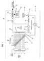
- FIG. 1 is a schematic block diagram of a transmitter that employs a tapped delay line multiplexer to generate a modulated encoded transmission signal in accordance with the preferred embodiments of the invention
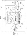
- FIG. 2 is a schematic block diagram of a receiver that employs a tapped delay line demultiplexer to receive and decode a modulated encoded transmission signal in accordance with a first preferred embodiment of the invention
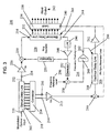
- FIG. 3 is a schematic block diagram of a receiver that employs a tapped delay line demultiplexer to receive and decode a modulated encoded transmission signal in accordance with a second preferred embodiment of the invention.
- a transmitter 10 is illustrated that is employed to generate an encoded serial data stream in accordance with the preferred embodiments of the present invention.
- the transmitter 10 receives parallel input data in the form of multiple bit words in an input latch 12.
- the number (m) of bits in each word can be arbitrarily chosen as desired but in one preferred embodiment is selected to be 16.
- Each of the bits in the word is clocked from the input latch 12 into a corresponding one of (m) inputs 13 of a pseudorandom number (PN) encoder 14 that encodes the bits into symbols in such a manner that each word can be identified in a data stream as will be discussed in more detail in conjunction with FIGs. 2 and 3. More particularly, the PN encoder 14 adds or subtracts a fixed number to each bit's value.
- the encoding process provides four possible symbol values. As an example, if the values 1, -1 are employed to represent the bit values 1 and 0, a value of 0.1 can be added or subtracted to these, thus giving the four possible symbol values 1.1, 0.9, -0.9 and -1.1.
- the encoded symbols are each fed into a corresponding one of (m) taps 15 of an (m) stage analog tapped electrical delay line 16 which acts as parallel to serial converter or multiplexer that converts the input parallel symbols of each word into an analog waveform comprised of a serial data stream.
- the serial data stream actually flows in opposite directions out a first serial output 18 and a second serial output 20 located at opposite ends of the delay line 16.
- the first output 18 supplies the data stream through a high pass filter 22 to an optical modulator 24.
- the modulator 24 modulates an output beam 26 from an optical source 28 (e.g., laser diode or the like) with the data stream to thereby generate a modulated optical output beam 30 that is suitable for transmission via a fiber optic cable. It will of course be understood, however, that other forms of modulation and transmission can be employed with the transmitter 10.
- the analog waveform also travels out the second serial output 20 from the delay line 16 for frequency control purposes as will be shown presently.
- the waveform passes though a low pass filter 32, which removes the high frequency serial symbol information from the waveform, and then through an amplifier 34 that conditions the waveform for detection by a frequency detector 36.
- the output waveform from the amplifier 34 is also fed back into the delay line 16 through its first output 18.
- the resulting feedback loop forms a ring oscillator 38 that oscillates at a fundamental frequency that is determined by the path length and delay characteristics of the delay line 16. This frequency is detected by the detector 36 and combined in an adder circuit 40 with a frequency reference level 42.
- the frequency reference level 42 is set equal to the desired transmission frequency of the data stream.
- an error signal is generated and fed through an integrator 44 to a control input 46 on the delay line 16 that controls its delay characteristics.
- a modulated optical input beam 102 which may be received through an optical fiber cable, for example, is detected by an optical detector 104, such as a PIN diode, and amplified by a trans-impedance amplifier 106 that serves an impedance matching function.
- the detected and amplified waveform is combined with a ring oscillator signal in a first adder circuit 108 and is then fed into an input 109 of a multiple stage analog tapped delay line 110.
- the analog tapped delay line 110 includes a group of (m) taps 112, one for each symbol in each received word, and acts as a serial to parallel converter or a demultiplexer to convert the incoming analog serial data stream into a parallel output data stream.
- the tapped delay line 110 also includes a serial output 113 that is employed for frequency calibration purposes as will be discussed in greater detail later.
- a sliding window correlator 114 is provided that continually samples each of the taps 112 to analyze the values of each stage in the delay line 110. More particularly, the sliding window correlator 114 continually computes the dot product of each symbol in the tapped delay line 110 and a corresponding symbol in a reference pseudorandom encoded word W 1 , ., W m . The results of these computations are combined in a second adder 116, which normally generates a steady magnitude output signal that is representative of background noise, but will generate a slightly greater magnitude spiked output signal whenever a complete PN encoded word is present in the tapped delay line 110.
- the PN synchronizing resonator loop 118 includes an amplifier 120 and an electrical delay line 121 such that an output 122 of the amplifier 120 is connected to an input 123 of the delay line 121.
- the electrical delay line 121 is selected to set the loop length exactly to the length of an (m) symbol word.
- the resonator loop 118 is needed because the magnitude of the spike received from the sliding window correlator 114 is typically only slightly higher than the background noise and is thus not sufficiently discernable to be used as a control input for the output latch 126.
- the resonator loop 118 solves this problem by effectively amplifying the spike, but not the background noise signal, until he spike is of great enough magnitude to actuate the output latch 126.
- a ring oscillator 130 is provided that is formed by the first adder circuit 108, the tapped delay line 110, a low pass filter 132, an amplifier 134 and an attenuator 136.
- An oscillating signal travels around the ring oscillator 130 and through the input 109 and serial output 113 of the tapped delay line 110 at a frequency that is dependent on the delay characteristics of the tapped delay line 110.
- a frequency tracking loop 138 is employed to maintain this frequency equal to that of the received symbols. As in the frequency tracking loop 48 of the transmitter 10 shown in FIG.
- a detector 140 generates a frequency signal that is combined in a third adder circuit 142 with a frequency reference level 144 that is preselected to be some multiple of the carrier frequency of the received data stream.
- the output of the adder circuit 142 is fed through an integrator 150, which then generates a control signal 152 that is connected to a control input 154 of the tapped delay line 110 and a control input 156 of the delay line 121.
- the delay characteristics of the tapped delay line 110 and the delay line 121 are adjusted to maintain synchronism of the incoming data stream with the resonator loop 118.
- the receiver 100 can also be fabricated on a single chip 160, which could be the same chip as the chip 50 used for the transmitter 10 in the case of a transceiver embodiment.
- FIG. 3 illustrates another embodiment of a receiver 200 in which an optical tapped delay line 202 and an optical sliding window correlator 204 are employed in place of the electrical versions of the same elements in the receiver 100 of FIG. 2. Otherwise, the receiver 200 includes many of the same elements of the receiver 100 and operates in much the same manner. These elements include a PN synchronization resonator loop 206, including an electrical delay line 208, adder circuit 210 and amplifier 212.
- the adder circuit 210 receives input from a first trans-impedance amplifier 213 that receives its input from the optical correlator 204 through a pair of detector diodes 214 and 216.
- the optical correlator 204 continually samples the values of the optical information in each stage of the optical delay line 202 through each of (m) taps 218.
- the optical delay line 202 receives a modulated optical waveform in an input 220 and passes this waveform, after a delay determined by the delay characteristics and length of the delay line 202, out a serial output 222.
- the waveform than passes through a third detector diode 224 and a second trans-impedance amplifier 226 and enters a ring oscillator loop 228 via an adder circuit 230.
- An analog tapped delay line 232 is provided in the oscillator loop 228 that receives the now electrical waveform through a serial input 234.
- the analog tapped delay line 232 includes a group of (m) parallel output taps 236 that are connected to an (m) bit parallel output latch 238.
- the output latch 238 is controlled by the signal in the resonator loop 206 through a control input 240.
- the latch 238 receives a control signal, it latches the symbols or bits that are present in the delay line 232 and provides them as a word output 242.
- the analog tapped delay line 232 also passes the incoming waveform through a serial output 244 to other elements that complete the ring oscillator 228, including a low pass filter 246, an amplifier 248 and an attenuator 250.
- the output from the amplifier 248 is also fed into a frequency detector 252 that forms part of a frequency tracking loop 254.
- a frequency reference level 256 is combined in an adder circuit 258 with the output from the detector 252.
- the output from the adder circuit 258 then passes through an integrator 260, which generates a control signal on an output 262 that is connected to a control input 264 of the analog tapped delay line 232 and a control input 266 of the electrical delay line 208 to control their frequency characteristics.
- Each of the loops in the receiver 200 including the resonator loop 206, the ring oscillator 228 and the frequency tracking loop 254 otherwise serves the same function as the corresponding elements in the receiver 100 of FIG. 2.
- the present invention employs delay lines and their tapped versions to achieve modulation and demodulation signal processing functions for a transmitter, receiver or transceiver, and is particularly suited for use with optical transceivers.
- Faster data acquisition by a receiver using a short data frame preamble is made possible with this invention's sliding window correlator.
- the correlator resolves the phase of the input waveform for all possible phase possibilities since the delay line in the PN sync resonator loop has the same electrical transit time as the tapped delay line which feeds the latch.
- the PN resonator loop which by design resonates at the frame rate, is driven by the output of the sliding window correlator which delivers a pulse to the loop each time a new word is centered in the tapped delay line.
- the PN resonator loop is able to provide a word clock to the output latch before any data is present.
- Environmental or age induced drift in the transit time of the tapped delay line of the PN sync resonator loop is calibrated out through the use of the frequency calibration loop imbedded within the tapped delay line. The accuracy of this calibration loop is sufficient to ensure that the data "eyes" are centered on the inputs of the output latch at the instant of phase recognition from the aforementioned sliding window correlator.
- the invention is therefore advantageous in that it provides high-speed acquisition for a burst data message using a feed-forward processor rather than a phased-lock-loop processor with a longer acquisition time. It therefore does not require acquisition times that are currently orders of magnitude longer than the messages.
- the opposite is true for the invention; it requires less than a 0.1% of the frame time. It requires no high-speed sampling circuitry that has an attendant high power and usually higher cost. Its lower power and smaller size enables a single chip demux at 40 Gbps for example. This would make a very attractive product especially for a market place that will be increasingly packetized and burst traffic oriented.
- the demultiplexed output is unambiguously referenced to the first bit in each PN coded frame. This eliminates the need for approximately 1/3 of the demux ASIC complexity downstream to resolve the inherent data ambiguity that is presented on the output of the prior art form.
Landscapes
- Engineering & Computer Science (AREA)
- Computer Networks & Wireless Communication (AREA)
- Signal Processing (AREA)
- Synchronisation In Digital Transmission Systems (AREA)
- Time-Division Multiplex Systems (AREA)
Applications Claiming Priority (2)
| Application Number | Priority Date | Filing Date | Title |
|---|---|---|---|
| US740766 | 1996-11-01 | ||
| US10/740,766 US7369600B2 (en) | 2003-12-22 | 2003-12-22 | Burst communications apparatus and method using tapped delay lines |
Publications (3)
| Publication Number | Publication Date |
|---|---|
| EP1548975A2 true EP1548975A2 (de) | 2005-06-29 |
| EP1548975A3 EP1548975A3 (de) | 2005-12-28 |
| EP1548975B1 EP1548975B1 (de) | 2009-05-06 |
Family
ID=34552798
Family Applications (1)
| Application Number | Title | Priority Date | Filing Date |
|---|---|---|---|
| EP04257977A Expired - Lifetime EP1548975B1 (de) | 2003-12-22 | 2004-12-20 | Impulsübertragungsvorrichtung und Impulsübertragungsverfahren mit Verzögerungsleitungen mit Abgriffen |
Country Status (3)
| Country | Link |
|---|---|
| US (1) | US7369600B2 (de) |
| EP (1) | EP1548975B1 (de) |
| DE (1) | DE602004020965D1 (de) |
Families Citing this family (7)
| Publication number | Priority date | Publication date | Assignee | Title |
|---|---|---|---|---|
| US7460785B2 (en) * | 2001-05-23 | 2008-12-02 | Lucent Technologies Inc. | Performance monitoring in an optical communication system |
| US7283744B2 (en) * | 2004-05-03 | 2007-10-16 | Lucent Technologies Inc. | Performance monitoring based on optical autocorrelation |
| US7558537B2 (en) * | 2005-06-07 | 2009-07-07 | Broadcom Corporation | Modified preamble for programmable transmitter |
| US9224016B2 (en) | 2010-07-01 | 2015-12-29 | Intelleflex Corporation | Automatic gain control and baseband preintegration to reduce computation requirements at lower data rates |
| US8976445B1 (en) * | 2012-03-02 | 2015-03-10 | University Of Southern California | Optical tunable tapped-delay-lines using wavelength conversion and chromatic dispersion based delays |
| US9762417B1 (en) * | 2016-09-28 | 2017-09-12 | Integra Research And Development, Llc | Adaptive equalization for vestigial sideband (VSB) transmissions |
| US11165539B1 (en) * | 2020-04-15 | 2021-11-02 | Mediatek Inc. | Method and apparatus for detecting word boundary between codewords in data stream transmitted via data channel of high definition multimedia interface |
Family Cites Families (10)
| Publication number | Priority date | Publication date | Assignee | Title |
|---|---|---|---|---|
| US4322819A (en) * | 1974-07-22 | 1982-03-30 | Hyatt Gilbert P | Memory system having servo compensation |
| EP0390226A1 (de) * | 1984-07-31 | 1990-10-03 | Yamaha Corporation | Absorptionsschaltung des Zitterns |
| US5016011A (en) * | 1988-06-10 | 1991-05-14 | General Electric Company | Increased performance of digital integrated circuits by processing with multiple-bit-width digits |
| US4993046A (en) * | 1988-06-24 | 1991-02-12 | Nippon Telegraph And Telephone Corporation | Coded modulation communication system |
| GB9108243D0 (en) * | 1991-04-17 | 1991-06-05 | Ladha Nizar | Self synchronizing automatic correlator |
| US5724007A (en) * | 1996-03-25 | 1998-03-03 | Cypress Semiconductor Corporation | Adjustable lock detector for a phase-locked loop circuit |
| US6275311B1 (en) * | 1997-06-30 | 2001-08-14 | Pirelli Cavi E Sistemi S.P.A. | Optical device for processing an optical digital signal |
| US6331976B1 (en) * | 1997-12-10 | 2001-12-18 | Texas Instruments Incorporated | Circuits system and methods for synchronization word detection in bitstream communications apparatus |
| IL127223A (en) * | 1998-11-24 | 2002-08-14 | Systel Dev And Ind Ltd | Power-line digital communication system |
| US6611217B2 (en) * | 1999-06-11 | 2003-08-26 | International Business Machines Corporation | Initialization system for recovering bits and group of bits from a communications channel |
-
2003
- 2003-12-22 US US10/740,766 patent/US7369600B2/en not_active Expired - Lifetime
-
2004
- 2004-12-20 DE DE602004020965T patent/DE602004020965D1/de not_active Expired - Lifetime
- 2004-12-20 EP EP04257977A patent/EP1548975B1/de not_active Expired - Lifetime
Also Published As
| Publication number | Publication date |
|---|---|
| EP1548975B1 (de) | 2009-05-06 |
| US20050135529A1 (en) | 2005-06-23 |
| US7369600B2 (en) | 2008-05-06 |
| EP1548975A3 (de) | 2005-12-28 |
| DE602004020965D1 (de) | 2009-06-18 |
Similar Documents
| Publication | Publication Date | Title |
|---|---|---|
| US7860400B2 (en) | Serializer/deserializers for use in optoelectronic devices | |
| US5239400A (en) | Technique for accurate carrier frequency generation in of DM system | |
| US7076177B1 (en) | Bit-rate independent optical receiver and method thereof | |
| US9294192B2 (en) | Method, system, and transceiver device for bi-directionally transmitting digital optical signals over an optical transmission link | |
| US5737366A (en) | Method and apparatus for receiving line encoded bursts of information | |
| EP0748077A2 (de) | Übertragungssystem mit asymmetrischem Pingpong-Verfahren | |
| EP1083685B1 (de) | Optische signalerzeugende Schaltung und optische Übertragungsleitung | |
| US8254340B2 (en) | Code division multiplex communication system | |
| US6178023B1 (en) | Optical telecommunication method providing a transmitting and receiving service channel | |
| US7369600B2 (en) | Burst communications apparatus and method using tapped delay lines | |
| US7095961B2 (en) | Optical communication system and optical receiver | |
| US7248802B2 (en) | Distribution of a synchronization signal in an optical communication system | |
| US20060088321A1 (en) | Closed loop RZ-DPSK alignment for optical communications | |
| JPH0828679B2 (ja) | 光フアイバデイジタルデ−タ伝送システム | |
| EP2260595B1 (de) | System und verfahren für passive optische netzwerke mit zweifacher geschwindigkeit | |
| US11552722B2 (en) | Precision time protocol using a coherent optical DSP frame | |
| JP3720537B2 (ja) | 光伝送システムにおいて補助チャンネルを伝送するための方法 | |
| US7567759B2 (en) | Optical apparatus | |
| EP4239911B1 (de) | Passives optisches netzwerk mit flexibler rate unter verwendung von verzögerungsmodulation | |
| KR101294516B1 (ko) | 버스트 모드 클럭 및 데이터 복원 장치 및 방법 | |
| US8463131B1 (en) | Method and apparatus for conveying timing information | |
| KR102016928B1 (ko) | 광전발진기를 이용한 송수신 동기화 방법 및 장치 | |
| Chan et al. | Real-time OC-192 all-optical bit-error monitoring system using inverted wavelength converter and optical NOR gate | |
| JP2007028301A (ja) | 光信号処理装置 | |
| JP2004524718A (ja) | 光伝送システム |
Legal Events
| Date | Code | Title | Description |
|---|---|---|---|
| PUAI | Public reference made under article 153(3) epc to a published international application that has entered the european phase |
Free format text: ORIGINAL CODE: 0009012 |
|
| AK | Designated contracting states |
Kind code of ref document: A2 Designated state(s): AT BE BG CH CY CZ DE DK EE ES FI FR GB GR HU IE IS IT LI LT LU MC NL PL PT RO SE SI SK TR |
|
| AX | Request for extension of the european patent |
Extension state: AL BA HR LV MK YU |
|
| PUAL | Search report despatched |
Free format text: ORIGINAL CODE: 0009013 |
|
| AK | Designated contracting states |
Kind code of ref document: A3 Designated state(s): AT BE BG CH CY CZ DE DK EE ES FI FR GB GR HU IE IS IT LI LT LU MC NL PL PT RO SE SI SK TR |
|
| AX | Request for extension of the european patent |
Extension state: AL BA HR LV MK YU |
|
| 17P | Request for examination filed |
Effective date: 20060421 |
|
| AKX | Designation fees paid |
Designated state(s): DE FR GB |
|
| GRAP | Despatch of communication of intention to grant a patent |
Free format text: ORIGINAL CODE: EPIDOSNIGR1 |
|
| GRAS | Grant fee paid |
Free format text: ORIGINAL CODE: EPIDOSNIGR3 |
|
| GRAA | (expected) grant |
Free format text: ORIGINAL CODE: 0009210 |
|
| AK | Designated contracting states |
Kind code of ref document: B1 Designated state(s): DE FR GB |
|
| REG | Reference to a national code |
Ref country code: GB Ref legal event code: FG4D |
|
| REF | Corresponds to: |
Ref document number: 602004020965 Country of ref document: DE Date of ref document: 20090618 Kind code of ref document: P |
|
| PLBE | No opposition filed within time limit |
Free format text: ORIGINAL CODE: 0009261 |
|
| STAA | Information on the status of an ep patent application or granted ep patent |
Free format text: STATUS: NO OPPOSITION FILED WITHIN TIME LIMIT |
|
| 26N | No opposition filed |
Effective date: 20100209 |
|
| PGFP | Annual fee paid to national office [announced via postgrant information from national office to epo] |
Ref country code: FR Payment date: 20110104 Year of fee payment: 7 |
|
| PGFP | Annual fee paid to national office [announced via postgrant information from national office to epo] |
Ref country code: GB Payment date: 20101221 Year of fee payment: 7 |
|
| REG | Reference to a national code |
Ref country code: GB Ref legal event code: 732E Free format text: REGISTERED BETWEEN 20110505 AND 20110511 |
|
| REG | Reference to a national code |
Ref country code: GB Ref legal event code: 732E Free format text: REGISTERED BETWEEN 20110512 AND 20110518 |
|
| REG | Reference to a national code |
Ref country code: FR Ref legal event code: TP Owner name: NORTHROP GRUMMAN SYSTEMS CORPORATION, US Effective date: 20120103 |
|
| REG | Reference to a national code |
Ref country code: DE Ref legal event code: R082 Ref document number: 602004020965 Country of ref document: DE Representative=s name: CHRISTOPHERSEN & PARTNER, DE |
|
| GBPC | Gb: european patent ceased through non-payment of renewal fee |
Effective date: 20111220 |
|
| REG | Reference to a national code |
Ref country code: FR Ref legal event code: ST Effective date: 20120831 |
|
| REG | Reference to a national code |
Ref country code: DE Ref legal event code: R081 Ref document number: 602004020965 Country of ref document: DE Owner name: NORTHROP GRUMMAN SYSTEMS CORPORATION, US Free format text: FORMER OWNER: NORTHROP GRUMMAN CORP., LOS ANGELES, US Effective date: 20120814 Ref country code: DE Ref legal event code: R082 Ref document number: 602004020965 Country of ref document: DE Representative=s name: CHRISTOPHERSEN & PARTNER, DE Effective date: 20120814 Ref country code: DE Ref legal event code: R081 Ref document number: 602004020965 Country of ref document: DE Owner name: NORTHROP GRUMMAN SYSTEMS CORPORATION, LOS ANGE, US Free format text: FORMER OWNER: NORTHROP GRUMMAN CORP., LOS ANGELES, CALIF., US Effective date: 20120814 Ref country code: DE Ref legal event code: R082 Ref document number: 602004020965 Country of ref document: DE Representative=s name: BUNGARTZ CHRISTOPHERSEN, PARTNERSCHAFT MBB PAT, DE Effective date: 20120814 |
|
| PG25 | Lapsed in a contracting state [announced via postgrant information from national office to epo] |
Ref country code: GB Free format text: LAPSE BECAUSE OF NON-PAYMENT OF DUE FEES Effective date: 20111220 |
|
| PG25 | Lapsed in a contracting state [announced via postgrant information from national office to epo] |
Ref country code: FR Free format text: LAPSE BECAUSE OF NON-PAYMENT OF DUE FEES Effective date: 20120102 |
|
| PGFP | Annual fee paid to national office [announced via postgrant information from national office to epo] |
Ref country code: DE Payment date: 20171211 Year of fee payment: 14 |
|
| REG | Reference to a national code |
Ref country code: DE Ref legal event code: R119 Ref document number: 602004020965 Country of ref document: DE |
|
| PG25 | Lapsed in a contracting state [announced via postgrant information from national office to epo] |
Ref country code: DE Free format text: LAPSE BECAUSE OF NON-PAYMENT OF DUE FEES Effective date: 20190702 |