EP1548923A2 - Control device and controlling method of inverter - Google Patents
Control device and controlling method of inverter Download PDFInfo
- Publication number
- EP1548923A2 EP1548923A2 EP04029578A EP04029578A EP1548923A2 EP 1548923 A2 EP1548923 A2 EP 1548923A2 EP 04029578 A EP04029578 A EP 04029578A EP 04029578 A EP04029578 A EP 04029578A EP 1548923 A2 EP1548923 A2 EP 1548923A2
- Authority
- EP
- European Patent Office
- Prior art keywords
- carrier wave
- frequency
- value
- inverter
- generating unit
- Prior art date
- Legal status (The legal status is an assumption and is not a legal conclusion. Google has not performed a legal analysis and makes no representation as to the accuracy of the status listed.)
- Granted
Links
Images




Classifications
-
- H—ELECTRICITY
- H02—GENERATION; CONVERSION OR DISTRIBUTION OF ELECTRIC POWER
- H02M—APPARATUS FOR CONVERSION BETWEEN AC AND AC, BETWEEN AC AND DC, OR BETWEEN DC AND DC, AND FOR USE WITH MAINS OR SIMILAR POWER SUPPLY SYSTEMS; CONVERSION OF DC OR AC INPUT POWER INTO SURGE OUTPUT POWER; CONTROL OR REGULATION THEREOF
- H02M7/00—Conversion of AC power input into DC power output; Conversion of DC power input into AC power output
- H02M7/42—Conversion of DC power input into AC power output without possibility of reversal
- H02M7/44—Conversion of DC power input into AC power output without possibility of reversal by static converters
- H02M7/48—Conversion of DC power input into AC power output without possibility of reversal by static converters using discharge tubes with control electrode or semiconductor devices with control electrode
- H02M7/53—Conversion of DC power input into AC power output without possibility of reversal by static converters using discharge tubes with control electrode or semiconductor devices with control electrode using devices of a triode or transistor type requiring continuous application of a control signal
- H02M7/537—Conversion of DC power input into AC power output without possibility of reversal by static converters using discharge tubes with control electrode or semiconductor devices with control electrode using devices of a triode or transistor type requiring continuous application of a control signal using semiconductor devices only, e.g. single switched pulse inverters
- H02M7/5387—Conversion of DC power input into AC power output without possibility of reversal by static converters using discharge tubes with control electrode or semiconductor devices with control electrode using devices of a triode or transistor type requiring continuous application of a control signal using semiconductor devices only, e.g. single switched pulse inverters in a bridge configuration
- H02M7/53871—Conversion of DC power input into AC power output without possibility of reversal by static converters using discharge tubes with control electrode or semiconductor devices with control electrode using devices of a triode or transistor type requiring continuous application of a control signal using semiconductor devices only, e.g. single switched pulse inverters in a bridge configuration with automatic control of output voltage or current
- H02M7/53875—Conversion of DC power input into AC power output without possibility of reversal by static converters using discharge tubes with control electrode or semiconductor devices with control electrode using devices of a triode or transistor type requiring continuous application of a control signal using semiconductor devices only, e.g. single switched pulse inverters in a bridge configuration with automatic control of output voltage or current with analogue control of three-phase output
-
- H—ELECTRICITY
- H02—GENERATION; CONVERSION OR DISTRIBUTION OF ELECTRIC POWER
- H02M—APPARATUS FOR CONVERSION BETWEEN AC AND AC, BETWEEN AC AND DC, OR BETWEEN DC AND DC, AND FOR USE WITH MAINS OR SIMILAR POWER SUPPLY SYSTEMS; CONVERSION OF DC OR AC INPUT POWER INTO SURGE OUTPUT POWER; CONTROL OR REGULATION THEREOF
- H02M7/00—Conversion of AC power input into DC power output; Conversion of DC power input into AC power output
- H02M7/42—Conversion of DC power input into AC power output without possibility of reversal
- H02M7/44—Conversion of DC power input into AC power output without possibility of reversal by static converters
- H02M7/48—Conversion of DC power input into AC power output without possibility of reversal by static converters using discharge tubes with control electrode or semiconductor devices with control electrode
- H02M7/53—Conversion of DC power input into AC power output without possibility of reversal by static converters using discharge tubes with control electrode or semiconductor devices with control electrode using devices of a triode or transistor type requiring continuous application of a control signal
- H02M7/537—Conversion of DC power input into AC power output without possibility of reversal by static converters using discharge tubes with control electrode or semiconductor devices with control electrode using devices of a triode or transistor type requiring continuous application of a control signal using semiconductor devices only, e.g. single switched pulse inverters
- H02M7/539—Conversion of DC power input into AC power output without possibility of reversal by static converters using discharge tubes with control electrode or semiconductor devices with control electrode using devices of a triode or transistor type requiring continuous application of a control signal using semiconductor devices only, e.g. single switched pulse inverters with automatic control of output wave form or frequency
- H02M7/5395—Conversion of DC power input into AC power output without possibility of reversal by static converters using discharge tubes with control electrode or semiconductor devices with control electrode using devices of a triode or transistor type requiring continuous application of a control signal using semiconductor devices only, e.g. single switched pulse inverters with automatic control of output wave form or frequency by pulse-width modulation
-
- H—ELECTRICITY
- H02—GENERATION; CONVERSION OR DISTRIBUTION OF ELECTRIC POWER
- H02P—CONTROL OR REGULATION OF ELECTRIC MOTORS, ELECTRIC GENERATORS OR DYNAMO-ELECTRIC CONVERTERS; CONTROLLING TRANSFORMERS, REACTORS OR CHOKE COILS
- H02P21/00—Arrangements or methods for the control of electric machines by vector control, e.g. by control of field orientation
- H02P21/05—Arrangements or methods for the control of electric machines by vector control, e.g. by control of field orientation specially adapted for damping motor oscillations, e.g. for reducing hunting
-
- H—ELECTRICITY
- H02—GENERATION; CONVERSION OR DISTRIBUTION OF ELECTRIC POWER
- H02M—APPARATUS FOR CONVERSION BETWEEN AC AND AC, BETWEEN AC AND DC, OR BETWEEN DC AND DC, AND FOR USE WITH MAINS OR SIMILAR POWER SUPPLY SYSTEMS; CONVERSION OF DC OR AC INPUT POWER INTO SURGE OUTPUT POWER; CONTROL OR REGULATION THEREOF
- H02M1/00—Details of apparatus for conversion
- H02M1/44—Circuits or arrangements for compensating for electromagnetic interference in converters or inverters
Definitions
- the present invention relates to a control device and a controlling method of an inverter that outputs a sinusoidal AC voltage supplied to a motor, by pulse width modulating (PWM) output of a DC power source, andmore specifically, the present invention relates to a technique for preventing occurrence of drawbacks caused by a carrier wave, without deteriorating motor efficiency.
- PWM pulse width modulating
- control device that detects current values of respective phases of a U phase, a V phase, and a W phase of a 3-phase brushless DC motor (hereinafter, “motor”) , and PID (proportion/integration/differentiation) controls detected values and generates PID control values so as to follow a sinusoidal current commandvalue, and switches on/off of a switching element structuring an inverter according to a relationship of magnitudes between the PID control values and a triangular wave-shaped carrier wave (hereinafter, "carrier wave”) in order to modulate the PID control values.
- carrier wave triangular wave-shaped carrier wave
- Such an inverter is generally called a triangular wave comparing type sine wave PWM inverter. It is known that, as a switching operation is carried out, this triangular wave comparing type sine wave PWM inverter generates drawbacks due to a frequency of the carrier wave, such as mechanical/electrical vibrations, noise, sound, EMI (Electromagnetic Interference) , andthe like. Therefore, as disclosed in Japanese Patent Application Laid-Open No. 2000-184729, in order to decrease mechanical/electrical vibrations due to the frequency of the carrier wave in conventional control devices, a peak value of a spectrum is kept low by randomly switching the frequency of the carrier wave and diffusing the spectrum of the carrier wave.
- the integration constant at the time of carrying out PID control depends on the frequency of the carrier wave. Therefore, if the frequency of the carrier wave is switched randomly as in the conventional control device, computation of the integration constant becomes complex, and a delay time of the PID control increases. Further, when controlling the inverter, usually, in order to compensate for a control delay time such as a delay time arising in order to sample currents of the respective phases, a delay time of the PID control, a delay time due to a control period, or the like, the control delay time is estimated, and delay compensation according to feed-forward is carried out. However, when the frequency of the carrier wave is switched randomly as in the conventional control device, it is difficult to estimate the control delay, and therefore, the control delay cannot be compensated for. For these reasons, according to conventional control devices, there are cases in which current cannot be controlled to a sine wave shape with sufficient accuracy, and the motor efficiency deteriorates.
- the present invention has been achieved in order to solve the above problems, and the invention provides a control device and a controlling method of an inverter that prevent occurrence of drawbacks due to a carrier wave, without deteriorating the motor efficiency.
- the present inventors have found, as a result of having repeatedly engaged in researches, that, by modulating the frequency of the carrier wave such that the frequency of the carrier wave changes in apredeterminedwaveform, the occurrence of drawbacks due to the carrier wave can be prevented without deteriorating the motor efficiency.
- One aspect of a control device of an inverter provides a control device of an inverter switching a positive electrode/negative electrode of a DC power source connected to a load by switching on/off of a switching element, and supplying a sinusoidal AC current to the load, comprising: a current command generating unit that generates a sinusoidal current command value; a triangular carrier wave generating unit that generates a triangular carrier wave; a PID control unit that PID controls an output value of the inverter to follow the current command value; a comparator that controls on/off operation of the switching element according to a relationship of magnitudes between an output value of the PID control unit and the carrier wave; and a carrier wave frequency generating unit that modulates a frequency such that a frequency of the carrier wave changes in a predetermined wave shape.
- Another aspect of a controllingmethod of an inverter according to the present invention provides a controlling method of an inverter switching a positive electrode/negative electrode of a DC power source connected to a load by switching on/off of a switching element, and supplying a sinusoidal AC current to the load, comprising the processes of: generating a sinusoidal current command value; generating a triangular carrier wave; PID controlling an output value of the inverter to follow the current command value; controlling on/off operation of the switching element according to a relationship of magnitudes between an output value of the inverter after the PID control and the carrier wave; and modulating a frequency such that a frequency of the carrier wave changes in a predetermined wave shape.
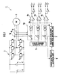
- the present invention can be applied to an inverter system, such as shown in Fig. 1, which has an inverter that supplies a sinusoidal AC current to a motor by PWM modulating output of a DC power source.
- Fig. 1 which has an inverter that supplies a sinusoidal AC current to a motor by PWM modulating output of a DC power source.
- an inverter system 1 that is the first embodiment of the present invention has, as main structural elements thereof, a PWM inverter 2, a 3-phase brushless DC motor (hereinafter, "motor") 3, current sensors 4a, 4b, 4c, a current command generating unit 5, PID control units 6a, 6b, 6c, a triangular wave-shaped carrier wave generating unit 7, comparators 8a, 8b, 8c, and a carrier wave frequency generating unit 9.
- the PWM inverter 2 has six switching elements Tu+, Tu-, Tv+, Tv-, Tw+, Tw- that, according to control of the comparators 8a, 8b, 8c, select a positive electrode or a negative electrode of a DC power source formed from a battery B and a capacitor C, and connect the selected electrode to the respective U phase, V phase, and W phase electrodes of the motor 3.
- These switching elements are structured by semiconductor elements such as IGBT (Insulated Gate Bipolar Transistors).
- the current sensors 4a, 4b, 4c respectively detect U phase, V phase, and W phase current values supplied from the PWM inverter 2 to the motor 3.
- the current command generating unit 5 generates sinusoidal current command values such that detected values of the current sensors 4a, 4b, 4c are converted into sinusoidal AC currents.
- the PID control units 6a, 6b, 6c PID control the detected values of the current sensors 4a, 4b, 4c, such that the detected values of the current sensors 4a, 4b, 4c follow the current command values that the current command generating unit 5 generates.
- the triangular wave-shaped carrier wave generating unit 7 generates a triangular wave-shaped carrier wave.
- the comparators 8a, 8b, 8c compare relationships of magnitudes between output values of the PID control units 6a, 6b, 6c and the triangular wave-shaped carrier wave, and, according to the relationships of magnitudes, input, to the PWM inverter 2, signals controlling on/off states of the switching elements Tu+, Tu-, Tv+, Tv-, Tw+, Tw- of the PWM inverter 2.
- the comparator 8a applies positive voltage to the U phase of the motor by controlling the Tu+, Tu- to be in an on state and an off state, respectively.
- the comparator 8a applies negative voltage to the U phase of the motor by controlling the Tu+, Tu- to be in an off state and an on state, respectively.
- the carrier wave frequency generating unit 9 varies a frequency f of the triangular carrier wave, according to timings of a maximum value and a minimum value of the triangular carrier wave inputted from the triangular wave-shaped carrier wave generating unit 7 (details are described later).
- the inverter system having such a structure can prevent the occurrence of drawbacks due to the carrier wave, without deteriorating the motor efficiency.
- operation of the carrier wave frequency generating unit 9 at the time of executing the frequency control processing is described in detail with reference to the flowchart of Fig. 2.
- the flowchart of Fig. 2 starts due to the triangular carrier wave (hereinafter, “carrier wave”) being inputted from the triangular carrier wave generating unit 7 to the carrier wave frequency generating unit 9, and the frequency control processing proceeds to processing at step S1.
- carrier wave triangular carrier wave
- the carrier wave frequency generating unit 9 determines whether the carrier wave inputted from the triangular carrier wave generating unit 7 is a maximum value or a minimum value (a peak). According to a determination that the carrier wave is a maximum value or a minimum value, the carrier wave frequency generating unit 9 advances the frequency control processing to processing at step S2.
- the carrier wave frequency generating unit 9 determines which of positive and negative a change value ⁇ of the frequency f of the carrier wave is. If the change value ⁇ is negative, the carrier wave frequency generating unit 9 advances the frequency control processing to processing at step S5. If the change value ⁇ is positive, the carrier wave frequency generating unit 9 advances the frequency control processing to processing at step S3.
- the carrier wave frequency generating unit 9 determines whether the frequency f reaches an upper limit value fmax. If results of determination show that the frequency f does not reach the upper limit value fmax, the carrier wave frequency generating unit 9 advances the frequency control processing to processing at step S7 so as not to change the change value ⁇ . If the frequency f reaches the upper limit value fmax, the carrier wave frequency generating unit 9 advances the frequency control processing to processing at step S4.
- the carrier wave frequency generating unit 9 transforms the change value ⁇ of the frequency f so that the frequency f is lowered from the upper limit value fmax.
- the processing at step S4 is thereby completed, and the frequency control processing advances from the processing at step S4 to the processing at step S7.
- the carrier wave frequency generating unit 9 determines whether the frequency f reaches a lower limit value fmin. If results of determination show that the frequency f does not reach the lower limit value fmin, the carrier wave frequency generating unit 9 advances the frequency control processing to the processing at step S7 so as not to change the change value ⁇ . If the frequency f reaches the lower limit value fmin, the carrier wave frequency generating unit 9 advances the frequency control processing to processing at step S6.
- the carrier wave frequency generating unit 9 transforms the change value ⁇ of the frequency f so that the frequency f is increased from the lower limit value fmin.
- the processing at step S6 is thereby completed, and the frequency control processing advances from the processing at step S6 to the processing at step S7.
- the carrier wave frequency generating unit 9 inputs, to the triangular wave-shaped carrier wave generating unit 7 and as the carrier wave frequency f of the next period, a value obtained by adding the change value ⁇ determined by the above processings to the current frequency f.
- the processing at step S7 is thereby completed, and the frequency control processing returns from the processing at step S7 to the processing at step S1.
- this series of frequency control processings as shown in Fig. 3, by reducing the carrier wave frequency f monotonically in a given section and increasing the carrier wave frequency f monotonically in a given section, the frequency of the carrier wave is modulated to a triangular shape, and a triangular carrier wave such as shown by the solid line in Fig. 4 can be generated.
- Figs. 3 and 4 show changes over time in the carrier wave frequency when the frequency of the carrier wave is modulated randomly and in a triangular shape, and changes over time in the carrier wave when the carrier wave frequency is constant (the dotted line) or is modulated in a triangular shape (the solid line) , respectively. While in this embodiment, as shown in Fig. 3, the frequency of the carrier wave is changed rectilinearly, the frequency may also be changed in any type of shape, such as, for example, changed in a curve, provided that an amount of change in the frequency f of the carrier wave does not become large, such as a case in which the frequency is changed randomly.
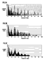
- Figs. 5A to 5C show results of simulation of spectra of the motor phase currents when the carrier wave frequency f is fixed and is modulated randomly and in a triangular shape.
- the peak of the higher harmonic of the motor phase current becomes smaller in the order of fixed, randomly modulating, and modulating in a triangular shape.
- a peak value when the carrier wave frequency f is fixed is 11 [dBA]
- 5 [dBA] in the case of randomly modulating and decreases to 0 [dBA] in the case of modulating in a triangular shape.
- the peak value when the carrier wave frequency is fixed is -1 [dBA]
- it is -4 [dBA] in the case of randomly modulating and decreases to -15 [dBA] in the case of modulating in a triangular shape.
- the frequency of the carrier wave is modulated in a triangular shape, as compared with a case in which the carrier wave frequency is modulated randomly as is the case conventionally, the peak value of the spectrum of the motor phase current can be lowered even more, and therefore, the occurrence of drawbacks due to the frequency of the carrier wave can be prevented even more effectively.
- the carrier wave frequency generating unit 9 modulates the frequency f of the carrier wave in a triangular shape. Therefore, as compared with a case in which the frequency f is modulated randomly, the occurrence of drawbacks due to the frequency of the carrier wave can be prevented even more effectively.
- the carrier wave frequency generating unit 9 modulates the carrier wave frequency f in a triangular shape. Therefore, the carrier wave frequency f can be computed and estimated easily. According to such a structure, because the time required for computation of the frequency f and the integration constant of the PID control can be kept to a minimum, a delay time in control due to computation time can be kept to a minimum, and the motor efficiency can be prevented from deteriorating.
- the control delay time can be estimated easily. According to such a structure, it is possible to prevent delay compensation by feed forward from being carried out, and to prevent the motor efficiency from deteriorating.
- the carrier wave frequency generating unit 9 determines whether the carrier wave inputted from the triangular carrier wave generating unit 7 is a maximum value or a minimum value. If the carrier wave is a peak of a maximum value or a minimum value, the carrier wave frequency generating unit transforms the change value ⁇ of the frequency of the carrier wave. Therefore, it is possible to prevent an inability to recompute the integration constant because the period of control changes in the midst of the period of the carrier wave, and to prevent accuracy of current control from deteriorating. Moreover, it is possible to prevent an inability to recompute control delay compensation because the period of control changes in the midst of the period of the carrier wave, and to prevent the accuracy of the current control from deteriorating.
- PID control is carried out on the sine wave command values of the respective phases of the U phase, the V phase, and the W phase.
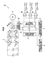
- a 3-phase ⁇ dq converting unit 22 converts the detected value of the current sensor into a value on a dq virtual axis
- the PID control unit 6 carries out PID control on the dq virtual axis.
- a dq ⁇ 3-phase converting unit 23 inversely converts the output value of the PID control unit 6 into a value on the 3-phase axis of the U phase, the V phase, and the W phase, and thereafter, inputs it to the comparator.
- the 3-phase ⁇ dq converting unit 22 converts the detected value of the current sensor into a value on the dq virtual axis, and the PID control unit 6 carries out PID control on the dq virtual axis.
- the current command value thereby becomes direct current on the dq virtual axis, and therefore, PID control can easily be realized in a digital form.
- the PID control unit 6, the triangular carrier wave generating unit 7, the carrier wave frequency generating unit 9, the 3-phase ⁇ dq converting unit 22, and the dq ⁇ 3-phase converting unit 23 can be structured in a digital form. Therefore, the inverter system can be structured inexpensively.
- an inverter system 31 according to a third embodiment of the present invention differs from the structure of the inverter system 21 according to the second embodiment with regard to the point that a delay compensating unit 21 is provided at the dq ⁇ 3-phase converting unit 23.
- the delay compensating unit 32 computes a control delay time, and corrects the current command value on the basis of results of computation.
- the delay compensating unit 32 computes the control delay time on the basis of the frequency f of the carrier wave. Therefore, the control delay can be accurately compensated for, and the motor efficiency can be prevented from deteriorating.
- the current command generating unit 5 generates a sinusoidal current command value, but may generate a current command value of a waveform obtained by adding a tertiary higher harmonic wave to a basic wave, or a waveform obtained by adding a triangular wave to a sine wave as shown in Fig. 8.
- a current command value of such a waveform By using a current command value of such a waveform, the efficiency of utilizing the voltage can be improved.
- the frequency of the carrier wave is modulated in a triangular shape, but may be modulated into any type of waveform provided that it is a waveform that can approximate a triangular shape. Specifically, even if the period of the carrier wave is modulated in a triangular shape, the frequency is triangular in first approximation, and therefore, technical effects that are similar to those of the above-described embodiments can be obtained.
- the processing of modulating the period of the carrier wave into a triangular shape can concretely be carried out according to the processing of the flowchart of Fig. 9. Namely, a period t of the carrier wave is increased by 1 (step S11).
- step S12 the period t is decreased by 1 (step S13).
- step S13 it is determined whether the change value ⁇ of the period t is greater than or equal to 0 (step S15). If the period t whose number is reduced is not 0, the routine returns to step S13. If it is determined, as a result of the processing of step S15, that the change value ⁇ of the period t is greater than or equal to 0, it is determined whether the period t reaches a maximum value ⁇ max (step S16). If the period t reaches the maximum value ⁇ max, the change value ⁇ of the period t is transformed (step S17).
- step S18 it is determined whether the period t reaches a minimum value ⁇ min (step S18) . If the period t reaches the minimum value ⁇ max, the change value ⁇ of the period t is transformed (step S19). The change value ⁇ determined by these processings is added to the current period ⁇ (step S20) , and thereafter, the processing again returns to the processing of step S11. Needless to say, other embodiments, examples, and operation techniques achieved by persons skilled in the art based on the above-described embodiments will all fall within the spirit of the present invention.
Landscapes
- Engineering & Computer Science (AREA)
- Power Engineering (AREA)
- Inverter Devices (AREA)
- Control Of Ac Motors In General (AREA)
Abstract
Description
Claims (6)
- A control device of an inverter (2) switching a positive electrode/negative electrode of a DC power source connected to a load by switching on/off of a switching element, and supplying a sinusoidal AC current to the load, comprising:a current command generating unit (5) that generates a sinusoidal current command value;a triangular carrier wave generating unit (7) that generates a triangular carrier wave;a PID control unit (6a, 6b, 6c) that PID controls an output value of the inverter to follow the current command value;a comparator (8a, 8b, 8c) that controls on/off operation of the switching element according to a relationship of magnitudes between an output value of the PID control unit (6a, 6b, 6c) and the carrier wave; anda carrier wave frequency generating unit (9) that modulates a frequency such that a frequency of the carrier wave changes in a predetermined wave shape.
- The control device of an inverter according to claim 1, wherein the carrier wave frequency generating unit (9) determines whether an amplitude of the carrier wave reaches a maximum value or a minimum value, and modulates the frequency by decreasing or increasing the frequency of the carrier wave according to the amplitude of the carrier wave reaching the maximum value or the minimum value.
- The control device of an inverter according to claim 1, wherein the load is a 3-phase AC motor (3) , and has a first converting unit (22) that converts the output value of the inverter into a value on a dq axis and inputs a converted value to the PID control unit, (6) and a second converting unit (23) that inversely converts the output value of the PID control unit (6) into a value on a 3-phase axis and inputs a converted value to the comparator (8a, 8b, 8c).
- The control device of an inverter according to claim 1, further comprising:a delay compensating unit (32) that computes a control delay time on the basis of the frequency of the carrier wave, and corrects the current command value on the basis of results of computation.
- The control device of an inverter according to claim 1, wherein the carrier wave frequency generating unit (9) modulates the frequency such that the frequency of the carrier wave changes in a triangular shape.
- A controlling method of an inverter (2) switching a positive electrode/negative electrode of a DC power source connected to a load by switching on/off of a switching element, and supplying a sinusoidal AC current to the load, comprising the processes of:generating a sinusoidal current command value;generating a triangular carrier wave;PID controlling an output value of the inverter to follow the current command value;controlling on/off operation of the switching element according to a relationship of magnitudes between an output value of the inverter after the PID control and the carrier wave; andmodulating a frequency such that a frequency of the carrier wave changes in a predetermined wave shape.
Applications Claiming Priority (2)
| Application Number | Priority Date | Filing Date | Title |
|---|---|---|---|
| JP2003431112A JP4085976B2 (en) | 2003-12-25 | 2003-12-25 | Inverter control device and control method |
| JP2003431112 | 2003-12-25 |
Publications (3)
| Publication Number | Publication Date |
|---|---|
| EP1548923A2 true EP1548923A2 (en) | 2005-06-29 |
| EP1548923A3 EP1548923A3 (en) | 2008-02-20 |
| EP1548923B1 EP1548923B1 (en) | 2010-08-11 |
Family
ID=34545043
Family Applications (1)
| Application Number | Title | Priority Date | Filing Date |
|---|---|---|---|
| EP04029578A Expired - Lifetime EP1548923B1 (en) | 2003-12-25 | 2004-12-14 | Control device and controlling method of inverter |
Country Status (4)
| Country | Link |
|---|---|
| US (1) | US6969968B2 (en) |
| EP (1) | EP1548923B1 (en) |
| JP (1) | JP4085976B2 (en) |
| DE (1) | DE602004028561D1 (en) |
Cited By (4)
| Publication number | Priority date | Publication date | Assignee | Title |
|---|---|---|---|---|
| WO2008141407A1 (en) * | 2007-05-17 | 2008-11-27 | Whirlpool S.A. | Method and system for reducing electromagnetic interference in a refrigeration system |
| EP1912323A3 (en) * | 2006-10-13 | 2010-02-24 | Nissan Motor Company Limited | Power converter and power conversion method |
| EP1850466A3 (en) * | 2006-04-26 | 2010-12-08 | Nissan Motor Co., Ltd. | Power converter control for reducing EMI noise by temporally changing the PWM carrier frequency |
| CN103187890A (en) * | 2011-12-27 | 2013-07-03 | 上海儒竞电子科技有限公司 | Control system of three-phase controlled rectifier |
Families Citing this family (17)
| Publication number | Priority date | Publication date | Assignee | Title |
|---|---|---|---|---|
| US8123130B2 (en) * | 1998-04-17 | 2012-02-28 | Remote Inc. | Remote ordering device |
| US7049778B2 (en) * | 2004-02-09 | 2006-05-23 | Nippon Yusoki Co., Ltd. | Inverter control apparatus and inverter control method |
| JP4677764B2 (en) * | 2004-11-08 | 2011-04-27 | 日産自動車株式会社 | Control device for pulse width modulation signal driving device |
| JP4761023B2 (en) * | 2005-03-15 | 2011-08-31 | 株式会社ジェイテクト | Brushless motor control device |
| US7688605B2 (en) * | 2005-07-27 | 2010-03-30 | Drs Sustainment Systems, Inc. | Systems and methods for reducing the magnitude of harmonics produced by a power inverter |
| JP4760465B2 (en) * | 2006-03-17 | 2011-08-31 | 日産自動車株式会社 | Power converter |
| JP5050395B2 (en) * | 2006-04-24 | 2012-10-17 | 日産自動車株式会社 | Power control apparatus and power control method |
| JP5169118B2 (en) * | 2007-10-02 | 2013-03-27 | 日産自動車株式会社 | Power conversion device and power conversion method |
| KR101244588B1 (en) * | 2008-04-28 | 2013-04-01 | 다이킨 고교 가부시키가이샤 | Inverter control device and power conversion device |
| JP5670904B2 (en) * | 2008-09-26 | 2015-02-18 | エクスレント エナジー テクノロジーズ リミテッド ライアビリティ カンパニー | Adaptive generation and control of arbitrary electrical waveforms in a grid-coupled power conversion system |
| US8693228B2 (en) | 2009-02-19 | 2014-04-08 | Stefan Matan | Power transfer management for local power sources of a grid-tied load |
| DE102009049055A1 (en) * | 2009-10-12 | 2011-04-14 | Continental Automotive Gmbh | Method and system for the electric drive of a vehicle |
| DE102011118044A1 (en) * | 2011-11-09 | 2013-05-16 | Conti Temic Microelectronic Gmbh | Method for controlling a motor by means of pulse width modulation (PWM) |
| WO2014192373A1 (en) * | 2013-05-27 | 2014-12-04 | 株式会社東芝 | Power conversion device, power conversion device control method, rotation sensorless control device, and rotation sensorless control device control method |
| JP5900470B2 (en) * | 2013-11-28 | 2016-04-06 | 株式会社安川電機 | Current source power converter |
| DE102014119502B3 (en) * | 2014-12-23 | 2016-03-24 | Sma Solar Technology Ag | Grid connected inverter, inverter arrangement and operating method for an inverter arrangement |
| US10566881B2 (en) | 2017-01-27 | 2020-02-18 | Franklin Electric Co., Inc. | Motor drive system including removable bypass circuit and/or cooling features |
Family Cites Families (17)
| Publication number | Priority date | Publication date | Assignee | Title |
|---|---|---|---|---|
| US3577052A (en) * | 1968-10-17 | 1971-05-04 | David Elvis Bauer | Ac motor control system with synchronous speed change |
| US3753063A (en) * | 1972-06-13 | 1973-08-14 | Gen Electric | Stabilizing means for an a-c motor drive |
| US3935518A (en) * | 1972-12-06 | 1976-01-27 | Vladimir Grigorievich Yatsuk | Method of eliminating self oscillations of an induction motor powered from a frequency changer and means for effecting same |
| US4186334A (en) * | 1978-02-07 | 1980-01-29 | Tokyo Shibaura Denki Kabushiki Kaisha | Control systems of alternating current motors |
| JPS5928148B2 (en) * | 1978-12-30 | 1984-07-11 | ファナック株式会社 | Induction motor operation control device |
| EP0159000B1 (en) * | 1984-04-16 | 1990-07-11 | Hitachi, Ltd. | Method and apparatus for controlling pwm inverters |
| US4663702A (en) * | 1984-10-12 | 1987-05-05 | Kabushiki Kaisha Toshiba | Power converter apparatus and control method thereof |
| US4651079A (en) * | 1985-11-29 | 1987-03-17 | Wills Frank E | Pulse width modulated inverter system for driving single phase a-c induction motor at a constant voltage/frequency ratio |
| JPS6373898A (en) * | 1986-09-12 | 1988-04-04 | Matsushita Electric Ind Co Ltd | Inverter |
| US5532569A (en) * | 1987-06-03 | 1996-07-02 | Hitachi, Ltd. | Inverter control apparatus |
| US4869592A (en) * | 1988-01-27 | 1989-09-26 | Bergh Ralph A | Method and apparatus for obtaining a digital measure of absolute rotation |
| KR0130537B1 (en) * | 1994-05-31 | 1998-04-09 | 이대원 | Brushless dc motor control system |
| DE59408662D1 (en) * | 1994-06-03 | 1999-09-30 | Inventio Ag | Quiet operation of a machine powered by a pulse inverter |
| JP3233005B2 (en) * | 1996-03-01 | 2001-11-26 | 株式会社日立製作所 | PWM controller |
| US5671130A (en) * | 1996-08-23 | 1997-09-23 | Allen-Bradley Company, Inc. | Method and apparatus for controlling voltage reflections using a motor controller |
| JP2000184729A (en) | 1998-12-17 | 2000-06-30 | Meidensha Corp | Method for modulating pwm inverter |
| JP2000184731A (en) * | 1998-12-18 | 2000-06-30 | Meidensha Corp | Power converter |
-
2003
- 2003-12-25 JP JP2003431112A patent/JP4085976B2/en not_active Expired - Fee Related
-
2004
- 2004-12-14 DE DE602004028561T patent/DE602004028561D1/en not_active Expired - Lifetime
- 2004-12-14 EP EP04029578A patent/EP1548923B1/en not_active Expired - Lifetime
- 2004-12-20 US US11/014,701 patent/US6969968B2/en not_active Expired - Lifetime
Cited By (6)
| Publication number | Priority date | Publication date | Assignee | Title |
|---|---|---|---|---|
| EP1850466A3 (en) * | 2006-04-26 | 2010-12-08 | Nissan Motor Co., Ltd. | Power converter control for reducing EMI noise by temporally changing the PWM carrier frequency |
| EP1912323A3 (en) * | 2006-10-13 | 2010-02-24 | Nissan Motor Company Limited | Power converter and power conversion method |
| US7729146B2 (en) | 2006-10-13 | 2010-06-01 | Nissan Motor Co., Ltd. | Power converter control and power conversion method |
| WO2008141407A1 (en) * | 2007-05-17 | 2008-11-27 | Whirlpool S.A. | Method and system for reducing electromagnetic interference in a refrigeration system |
| CN103187890A (en) * | 2011-12-27 | 2013-07-03 | 上海儒竞电子科技有限公司 | Control system of three-phase controlled rectifier |
| CN103187890B (en) * | 2011-12-27 | 2015-05-06 | 上海儒竞电子科技有限公司 | Control system of three-phase controlled rectifier |
Also Published As
| Publication number | Publication date |
|---|---|
| US20050140330A1 (en) | 2005-06-30 |
| JP4085976B2 (en) | 2008-05-14 |
| EP1548923A3 (en) | 2008-02-20 |
| DE602004028561D1 (en) | 2010-09-23 |
| JP2005192336A (en) | 2005-07-14 |
| US6969968B2 (en) | 2005-11-29 |
| EP1548923B1 (en) | 2010-08-11 |
Similar Documents
| Publication | Publication Date | Title |
|---|---|---|
| US6969968B2 (en) | Control device and controlling method of inverter | |
| US8710781B2 (en) | Power conversion device and method for controlling thereof | |
| CN104685778B (en) | Method for controlling power conversion apparatus | |
| EP1919064A2 (en) | Power supply circuit and control circuit for use in the same | |
| JP5423777B2 (en) | Converter control device for vehicle | |
| US9634602B2 (en) | Three-phase inverter apparatus and control method thereof | |
| KR20160122923A (en) | Apparatus and method for generating offset voltage of 3-phase inverter | |
| CN107148729A (en) | Charge-discharge circuit, the control method of charge-discharge circuit, the control device and direct power converter of charge-discharge circuit | |
| CN111200144B (en) | Current control system, fuel cell system, and control method for boost converter | |
| KR20160108216A (en) | Conversion device | |
| WO2012117642A1 (en) | Electrical power conversion device, electrical power conversion system, and motor inverter | |
| GB2421090A (en) | Voltage source inverter control method | |
| JPH10327576A (en) | AC-DC converter | |
| JPH1127951A (en) | PWM inverter control device | |
| US11682998B2 (en) | Motor control method and motor control apparatus | |
| JP6873357B1 (en) | Multiphase converter controller | |
| JP7211097B2 (en) | Power control method and power control device | |
| JP2018137840A (en) | Power factor correction circuit | |
| JP2004064947A (en) | Voltage controller for voltage-type pwm inverter | |
| WO2015097533A1 (en) | Motor control system, motor control device, and motor control method | |
| Kwon et al. | Three-phase PWM synchronous rectifiers without line-voltage sensors | |
| JPH05176553A (en) | Inverter control method of non-interruption power supply apparatus and non-interruption power supply apparatus | |
| JP2007325365A (en) | Grid-connected inverter device | |
| JP2006166628A (en) | Power converter control method | |
| JPH0824426B2 (en) | Pulse width modulation type inverter device |
Legal Events
| Date | Code | Title | Description |
|---|---|---|---|
| PUAI | Public reference made under article 153(3) epc to a published international application that has entered the european phase |
Free format text: ORIGINAL CODE: 0009012 |
|
| 17P | Request for examination filed |
Effective date: 20041214 |
|
| AK | Designated contracting states |
Kind code of ref document: A2 Designated state(s): AT BE BG CH CY CZ DE DK EE ES FI FR GB GR HU IE IS IT LI LT LU MC NL PL PT RO SE SI SK TR |
|
| AX | Request for extension of the european patent |
Extension state: AL BA HR LV MK YU |
|
| PUAL | Search report despatched |
Free format text: ORIGINAL CODE: 0009013 |
|
| AK | Designated contracting states |
Kind code of ref document: A3 Designated state(s): AT BE BG CH CY CZ DE DK EE ES FI FR GB GR HU IE IS IT LI LT LU MC NL PL PT RO SE SI SK TR |
|
| AX | Request for extension of the european patent |
Extension state: AL BA HR LV MK YU |
|
| AKX | Designation fees paid |
Designated state(s): DE FR GB |
|
| 17Q | First examination report despatched |
Effective date: 20081203 |
|
| GRAP | Despatch of communication of intention to grant a patent |
Free format text: ORIGINAL CODE: EPIDOSNIGR1 |
|
| GRAS | Grant fee paid |
Free format text: ORIGINAL CODE: EPIDOSNIGR3 |
|
| GRAA | (expected) grant |
Free format text: ORIGINAL CODE: 0009210 |
|
| AK | Designated contracting states |
Kind code of ref document: B1 Designated state(s): DE FR GB |
|
| REG | Reference to a national code |
Ref country code: GB Ref legal event code: FG4D |
|
| REF | Corresponds to: |
Ref document number: 602004028561 Country of ref document: DE Date of ref document: 20100923 Kind code of ref document: P |
|
| PLBE | No opposition filed within time limit |
Free format text: ORIGINAL CODE: 0009261 |
|
| STAA | Information on the status of an ep patent application or granted ep patent |
Free format text: STATUS: NO OPPOSITION FILED WITHIN TIME LIMIT |
|
| 26N | No opposition filed |
Effective date: 20110512 |
|
| REG | Reference to a national code |
Ref country code: DE Ref legal event code: R097 Ref document number: 602004028561 Country of ref document: DE Effective date: 20110512 |
|
| PGFP | Annual fee paid to national office [announced via postgrant information from national office to epo] |
Ref country code: DE Payment date: 20141209 Year of fee payment: 11 Ref country code: GB Payment date: 20141210 Year of fee payment: 11 |
|
| PGFP | Annual fee paid to national office [announced via postgrant information from national office to epo] |
Ref country code: FR Payment date: 20141208 Year of fee payment: 11 |
|
| REG | Reference to a national code |
Ref country code: DE Ref legal event code: R119 Ref document number: 602004028561 Country of ref document: DE |
|
| GBPC | Gb: european patent ceased through non-payment of renewal fee |
Effective date: 20151214 |
|
| REG | Reference to a national code |
Ref country code: FR Ref legal event code: ST Effective date: 20160831 |
|
| PG25 | Lapsed in a contracting state [announced via postgrant information from national office to epo] |
Ref country code: GB Free format text: LAPSE BECAUSE OF NON-PAYMENT OF DUE FEES Effective date: 20151214 Ref country code: DE Free format text: LAPSE BECAUSE OF NON-PAYMENT OF DUE FEES Effective date: 20160701 |
|
| PG25 | Lapsed in a contracting state [announced via postgrant information from national office to epo] |
Ref country code: FR Free format text: LAPSE BECAUSE OF NON-PAYMENT OF DUE FEES Effective date: 20151231 |