EP1548840A1 - Organic thin-film transistor and method for manufacturing organic thin-film transistor - Google Patents
Organic thin-film transistor and method for manufacturing organic thin-film transistor Download PDFInfo
- Publication number
- EP1548840A1 EP1548840A1 EP03794125A EP03794125A EP1548840A1 EP 1548840 A1 EP1548840 A1 EP 1548840A1 EP 03794125 A EP03794125 A EP 03794125A EP 03794125 A EP03794125 A EP 03794125A EP 1548840 A1 EP1548840 A1 EP 1548840A1
- Authority
- EP
- European Patent Office
- Prior art keywords
- film transistor
- organic
- organic thin
- oligomer
- semiconductor layer
- Prior art date
- Legal status (The legal status is an assumption and is not a legal conclusion. Google has not performed a legal analysis and makes no representation as to the accuracy of the status listed.)
- Withdrawn
Links
Images
Classifications
-
- H—ELECTRICITY
- H10—SEMICONDUCTOR DEVICES; ELECTRIC SOLID-STATE DEVICES NOT OTHERWISE PROVIDED FOR
- H10K—ORGANIC ELECTRIC SOLID-STATE DEVICES
- H10K71/00—Manufacture or treatment specially adapted for the organic devices covered by this subclass
- H10K71/10—Deposition of organic active material
-
- H—ELECTRICITY
- H10—SEMICONDUCTOR DEVICES; ELECTRIC SOLID-STATE DEVICES NOT OTHERWISE PROVIDED FOR
- H10K—ORGANIC ELECTRIC SOLID-STATE DEVICES
- H10K10/00—Organic devices specially adapted for rectifying, amplifying, oscillating or switching; Organic capacitors or resistors having potential barriers
- H10K10/40—Organic transistors
- H10K10/46—Field-effect transistors, e.g. organic thin-film transistors [OTFT]
- H10K10/462—Insulated gate field-effect transistors [IGFETs]
- H10K10/464—Lateral top-gate IGFETs comprising only a single gate
-
- H—ELECTRICITY
- H10—SEMICONDUCTOR DEVICES; ELECTRIC SOLID-STATE DEVICES NOT OTHERWISE PROVIDED FOR
- H10K—ORGANIC ELECTRIC SOLID-STATE DEVICES
- H10K10/00—Organic devices specially adapted for rectifying, amplifying, oscillating or switching; Organic capacitors or resistors having potential barriers
- H10K10/40—Organic transistors
- H10K10/46—Field-effect transistors, e.g. organic thin-film transistors [OTFT]
- H10K10/462—Insulated gate field-effect transistors [IGFETs]
- H10K10/466—Lateral bottom-gate IGFETs comprising only a single gate
-
- H—ELECTRICITY
- H10—SEMICONDUCTOR DEVICES; ELECTRIC SOLID-STATE DEVICES NOT OTHERWISE PROVIDED FOR
- H10K—ORGANIC ELECTRIC SOLID-STATE DEVICES
- H10K85/00—Organic materials used in the body or electrodes of devices covered by this subclass
- H10K85/10—Organic polymers or oligomers
- H10K85/111—Organic polymers or oligomers comprising aromatic, heteroaromatic, or aryl chains, e.g. polyaniline, polyphenylene or polyphenylene vinylene
- H10K85/113—Heteroaromatic compounds comprising sulfur or selene, e.g. polythiophene
-
- H—ELECTRICITY
- H10—SEMICONDUCTOR DEVICES; ELECTRIC SOLID-STATE DEVICES NOT OTHERWISE PROVIDED FOR
- H10K—ORGANIC ELECTRIC SOLID-STATE DEVICES
- H10K99/00—Subject matter not provided for in other groups of this subclass
-
- H—ELECTRICITY
- H10—SEMICONDUCTOR DEVICES; ELECTRIC SOLID-STATE DEVICES NOT OTHERWISE PROVIDED FOR
- H10K—ORGANIC ELECTRIC SOLID-STATE DEVICES
- H10K85/00—Organic materials used in the body or electrodes of devices covered by this subclass
- H10K85/10—Organic polymers or oligomers
- H10K85/111—Organic polymers or oligomers comprising aromatic, heteroaromatic, or aryl chains, e.g. polyaniline, polyphenylene or polyphenylene vinylene
- H10K85/115—Polyfluorene; Derivatives thereof
-
- H—ELECTRICITY
- H10—SEMICONDUCTOR DEVICES; ELECTRIC SOLID-STATE DEVICES NOT OTHERWISE PROVIDED FOR
- H10K—ORGANIC ELECTRIC SOLID-STATE DEVICES
- H10K85/00—Organic materials used in the body or electrodes of devices covered by this subclass
- H10K85/10—Organic polymers or oligomers
- H10K85/151—Copolymers
Definitions
- the present invention relates to an organic thin-film transistor and a manufacturing method thereof.
- organic thin-film transistor employing an organic semiconducting compound as a semiconductor channel has been studied.
- the organic semiconducting compound is easy in processing and high affinity to a plastic sheet support, as compared with an inorganic semiconducting compound, and therefore, is preferred in its application to a thin-film device.
- the technique proposed in the patent document requires high temperature of at least 250 °C in order to transit the semiconducting polymer to a liquid phase, and therefore, requires, as a support, colored heat resistant films such as polyimide film or heat resistant materials such as glass plates. Further, this requires a process of forming an orientation film adjacent to the semiconductor layer, which complicates constitution of a semiconductor element.
- a modified FET structure has been proposed in Japanese Patent O.P.I. Publication No. 2000-260999, which employs an organic-inorganic hybrid material as a semiconductor channel.
- a semiconductor element with high mobility is proposed which employs a self-organizing (self-assemble) semiconductor material, which actually requires complex processes to prepare the semiconductor material.
- An object of the invention is to provide an organic thin film transistor with a high mobility of carriers (electrons or holes), which is capable of employing a sheet of conventional plastics or transparent resins as the support, and a manufacturing method thereof.
- the object of the invention can be attained according to the following constitutions.
- An organic thin-film transistor comprising a support and provided thereon, a gate electrode, an insulation layer, a source electrode, a drain electrode, and an organic semiconductor layer, the support comprising at least one of resins, and the organic semiconductor layer containing at least one of organic semiconducting materials, wherein a phase transition temperature of one of the organic semiconducting materials is not more than a glass transition point of one of the resins.
- a manufacturing process of an organic thin-film transistor comprising a support and provided thereon, a gate electrode, an insulation layer, a source electrode, a drain electrode, and an organic semiconductor layer, the support comprising at least one of resins, and the organic semiconductor layer containing at least one of organic semiconducting materials, wherein a phase transition temperature of one of the organic semiconducting materials is not more than a glass transition point of one of the resins, the process comprising the steps of providing a solution or dispersion solution of the organic semiconducting material, and coating the solution or dispersion solution on the support or on the insulation layer to form the organic semiconductor layer.
- phase transition temperature is in the range of from 100 to 240 °C.
- An organic thin-film transistor comprising a support and provided thereon, a gate electrode, an insulation layer, a source electrode, a drain electrode, and an organic semiconductor layer, the support comprising at least one of resins, and the organic semiconductor layer containing at least one of organic semiconducting materials, wherein a phase transition temperature of at least one of the organic semiconducting materials is not more than a glass transition point of at least one of the resins.
- organic thin-film transistor of any one of items 2-1 through 2-7 above, wherein at least one of the organic semiconducting materials is a ⁇ -conjugated polymer or oligomer.
- the organic thin-film transistor of item 2-10 above, wherein the alkyl group of the poly(3-alkylthiophene) having a regioregular structure is an alkyl group having a carbon atom number of from 4 to 15.
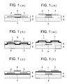
- Figures 1(a) through 1(f) show sectional views of embodiments of the organic thin-film transistor of the invention.
- the organic thin-film transistor comprises a support and provided thereon, a gate electrode, an insulation layer, a source electrode, a drain electrode, and an organic semiconductor layer, the support comprising at least one of resins, and the organic semiconductor layer containing at least one of organic semiconducting materials, wherein a phase transition temperature of one of the resins is not more than a glass transition point of one of the organic semiconducting materials.
- the organic semiconducting compound known ⁇ -conjugated polymer or oligomer and other organic semiconducting compound as described later are used.
- the ⁇ -conjugated oligomer in the invention implies one having in the molecule a repeating monomer unit number of from 2 to 20 (a polymerization degree of from 2 to 20).
- the ⁇ -conjugated polymer in the invention implies one having a weight average molecular weight of preferably from 1,000 to 500,000, and more preferably from 5,000 to 100,000.
- Examples of the ⁇ -conjugated polymers include polypyrroles such as polypyrrole, poly(N-substituted pyrrole), poly(3-substituted pyrrole), and poly(3,4-disubstituted pyrrole); polythiophenes such as polythiophene, poly(3-substituted thiophene), poly(3,4-disubstituted thiophene), and polybenzothiophene; polyisothianaphthenes such as polyisothianaphthene; polythienylenevinylenes such as polythienylenevinylene; poly(p-phenylenevinylenes) such as poly(p-phenylenevinylene); polyanilines such as polyaniline, poly(N-substituted aniline), poly(3-substituted aniline), and poly(2,3-substituted aniline); polyacetylnenes such as polyace
- ⁇ -conjugated oligomers examples include oligomers having the same repeating units as the above polymers, for example, thiophene hexamers including ⁇ -sexithiophene, ⁇ , ⁇ -dihexyl- ⁇ -sexithiophene, ⁇ , ⁇ ,-dihexyl- ⁇ -quinquethiophene, and ⁇ , ⁇ -bis(3-butoxypropyl)- ⁇ -sexithiophene.
- organic semiconducting compound examples include styrylbenzene derivatives; polyacenes such as naphthacene, pentacene, hexacene, heptacene, dibenzopentacene, tertabenzopentacene, pyrene, dibenzopyrene, chrysene, perylene, coronene, terylene, ovalene, quoterylene, and circumanthracene; derivatives (such as triphenodioxazine, triphenodithiazine, hexacene-6,15-quinone) in which some of carbon atoms of polyacenes are substituted with atoms such as N, S, and O or with a functional group such as a carbonyl group; and polycyclic condensation products described in Japanese Patent O.P.I.
- metallophthalocyanines such as copper phthalocyanine, and fluorine-substituted copper phthalocyanines described in Japanese Patent O.P.I. Publication No. 11-251601; tetracarboxylic acid diimides of condensed ring compounds including naphthalene tetracarboxylic acid imides such as naphthalene 1,4,5,8-teracarboxylic acid diimide, N,N'-bis(4-trifluoromethylbenzyl)naphthalene 1,4,5,8-tretracarboxylic acid diimide, N,N'-bis(1H,1H-perfluoroctyl)naphthalene 1,4,5,8-tetracarboxylic acid diimide derivatives, N,N'-bis(1H,1H-perfluorobutyl)naphthalene 1,4,5,8-tetracarboxylic acid diimide derivatives, N,N'-bis(1H,1H-
- organic semiconducting compounds may be organic molecular complexes such as a tetrathiafulvalene (TTF)-tetracyanoquinodimethane (TCNQ) complex, a bisethylenetetrathiafulvalene (BEDTTTF)-perchloric acid complex, a BEDTTTF-iodine complex, and a TCNQ-iodine complex.
- organic molecular complexes such as a tetrathiafulvalene (TTF)-tetracyanoquinodimethane (TCNQ) complex, a bisethylenetetrathiafulvalene (BEDTTTF)-perchloric acid complex, a BEDTTTF-iodine complex, and a TCNQ-iodine complex.
- TTF tetrathiafulvalene
- TCNQ bisethylenetetrathiafulvalene
- BEDTTTF bisethylenetetrathiafulvalene
- organic semiconducting compounds preferably employed is at least one selected from the group consisting of ⁇ -conjugate polymers or oligomers, which have thiophene, vinylene, thienylenevinylene, phenylenevinylene, p-phenylene, their substitution product or at least two kinds thereof as a repeating unit, and condensed polycyclic aromatic compounds such as pentacene.
- Materials are preferred which form a stereo-regular structure by incorporating a substituent such as alkyl having a carbon atom number of from 4 to 15 in at least one portion of the repeating unit. Incorporation of a substituent such as alkyl can increase solubility to an organic solvent of organic semiconducting compounds, and give regularity to a high order structure of the polymer from which organic semiconductor layer is formed.
- a homopolymer, a copolymer, a homo-oligomer, or a co-oligomer containing a thiophene ring is preferred, and a homopolymer, a copolymer, a homo-oligomer, or a co-oligomer containing a unit, in which two or more of 3-alkylthiophene rings are regio-regularly connected in series, is more preferred.
- a manufacturing method of the organic thin-film transistor (or a manufacturing method of the thin film) of the invention will be described later.
- the manufacturing method of the organic thin-film transistor comprising providing a coating solution containing the organic semiconducting material and coating the solution on a support, is preferably used in precisely controlling the thin film formation and improving productivity.
- the alkyl group of the 3-alkylthiophene is preferably a straight chained alkyl group having a carbon atom number of from 4 to 15, in increasing solubility of the organic semiconducting material in various solvents used in the coating solution and in forming a coated film so that the thiophene ring in the semiconducting material in the coated film exhibits a specific regio-regularity; and more preferably a straight chained alkyl group having a carbon atom number of not less than 6, and preferably from 8 to 12, in adjusting the phase transition temperature of the organic semiconducting material to liquid crystal phase to not more than 240 °C and in making it possible to used a conventional plastic sheet as the support of the organic thin-film transistor.
- poly(3-alkylthiophene) examples include poly(3-hexylthiophene), poly(3-octylthiophene), poly(3-decylthiophene), and oligo(3-hexylthiophene) (for example, octamer to hexadecamer), each being regioregular, and an oligomer or polymer represented by the following formulae.
- polythiophene used in the invention there are those disclosed in Japanese Patent O.P.I. Publication No. 10-190001, "Nature”, 41 , p. 685 (1999), or Applied Phys. Lett., 69 , p. 4108 (1996).
- the weight average molecular weight of the thiophene homopolymer or copolymer used in the invention is preferably from 1,000 to 500,000, and more preferably from 5000 to 100,000.
- a phase transition temperature (°C) of at least one of the organic semiconducting materials used is not more than a glass transition point (°C) of at least one of resins constituting a support described later in obtaining the effects of the invention that the organic thin-film transistor has a high carrier (electron or hole) mobility and can employ conventional plastic materials or transparent resins as materials for the support.
- phase transition temperature of organic semiconducting materials herein referred to implies a melting point, a softening point, a secondary transition temperature (fro example, a glass transition point), or a phase transition point to liquid crystal phase.
- the phase transition temperature (liquid phase transition point) of the organic semiconducting materials used in the invention is preferably from 100 to 240 °C.
- the melting point or liquid phase transition point of the organic semiconducting materials is not more than a glass transition point (°C) of at least one of resins constituting the support.
- the melting point can be measured through an automatic melting point apparatus available on the market, and the phase transition point can be measured through a differential scanning colorimeter (DSC) available on the market.
- the phase transition behavior can be observed through a polarization microscope (POM).
- POM polarization microscope
- the higher order structure, relationship between crystallinity or liquid crystallinity and the molecular structure can be analyzed through X-ray diffraction (XRD).
- the methods for forming the organic semiconductor layer include a vacuum deposition method, a molecular beam epitaxial growth method, an ion cluster beam method, a low energy ion beam method, an ion plating method, a CVD method, a sputtering method, a plasma polymerization method, an electrolytic polymerization method, a chemical polymerization method, a spray coating method, a spin coating method, a blade coating method, a dip coating method, a casting method, a roll coating method, an bar coating method, a die coating method, an ink-jet method, and an LB method. These methods may be used according to kinds of materials used.
- the spin coating method, blade coating method, dip coating method, roll coating method, bar coating method, die coating method and ink-jet method are preferred from the viewpoint of productive efficiency, which can simply and accurately form the layer employing a solution of organic semiconductor materials.
- an organic semiconductor layer may be formed, jetting a solution or dispersion of the organic semiconductor by ink jet and drying.
- the organic semiconductor layer after formed, is preferably subjected to heat treatment.
- the organic semiconductor layer is heated to not less than the phase transition temperature or preferably not less than the melting point of the organic semiconducting material to transit the phase, and cooled to solidify, whereby an organic semiconductor layer is formed.
- the cooling is gradually carried out at a cooling speed of not more than 5 °C/ sec., and preferably from 0.1 °C/sec to 1 °C/sec.
- the effect that the carrier mobility of the organic semiconductor layer is increased due to the gradual cooling is obtained.
- a support having a glass transition point satisfying the conditions described above exhibits the unexpected result that the mobility is further increased.
- the thickness of the organic semiconductor layer is not specifically limited.
- the thickness of an organic semiconductor layer comprised of the organic semiconductor materials often has a great influence on properties of the resultant transistor. Accordingly, the thickness of the layer differs due to kinds of the organic semiconductor materials used, but it is preferably not more than 1 ⁇ m, and more preferably from 10 to 300 nm.
- a glass transition point (S °C) of at least one of resins constituting the support is not less than a phase transition temperature (T °C) of at least one of the organic semiconducting materials used, i.e., S (°C) ⁇ T (°C).
- the support is comprised of glass or a flexible resin sheet.
- a plastic film as the sheet.
- materials for the plastic film include polyesters such as polyethylene terephthalate (PET) and polyethylene naphthalate (PEN); polyvinylidene chloride; polyvinyl alcohol; polyethylene vinyl alcohol; syndiotactic polystyrene; polyethylene; polypropylene; cellophane; polyethersulfone (PES); polyetherimide PEI); polyether ether ketone; polysulfone (PSF); polyphenylene sulfide; polyallylate; polyimide; polyamide; polycarbonate (PC); norbornene resin (cyclolefin resin); polymethylpentene; fluorine-contained resin; acryl resin; ellulose esters such as cellulose triacetate (TAC), cellulose diacetate, cellulose acetate propionate (CAP), cellulose acetate butyrate, cellulose acetate phthalate,
- TAC
- polyethersulfone PES
- polyetherimide PEI polyether ether ketone
- polysulfone PSF
- norbornene resin norbornene resin
- hest resistant polycarbonate cellulose triacetate (TAC)
- DAC cellulose diacetate
- CAP cellulose acetate propionate
- cellulose acetate butyrate cellulose acetate phthalate
- cellulose nitrate are preferred.
- the plastic film can be subjected to surface treatment or surface coating employing a conventional method.
- a co-deposit layer of silicon oxide and aluminum oxide or a layer or multi-layers of a mixture of metal oxides such as silicon oxide and aluminum oxide according to a plasma method may be provided on the film as a gas barrier layer.
- a metal film deposited with metal such as aluminum may be laminated on the above plastic film to obtain a composite film. Further, metal oxide particles may be incorporated in the plastic film.
- plastic film makes it possible to decrease weight, to enhance portability, and to enhance durability against impact due to its flexibility, as compared to glass.
- the glass transition point of resins constituting the support can be measured through a differential scanning colorimeter (DSC) or a dynamic viscoelasticity meter.
- DSC differential scanning colorimeter
- the glass transition point of the resins used in the invention is preferably not less than 110 °C, and more preferably not less than 150 °C.
- the glass transition point of the resins used in the invention is preferably not more than 350 °C.
- an orientation layer is preferably provided adjacent to the organic semiconductor layer, the orientation film having capability of orientating the organic semiconducting material in a specific direction.
- orientation layer in the invention conventional ones used in conventional liquid crystal display can be used, which are disclosed in for example, Japanese Patent O.P.I. Publication Nos. 9-194725 and 9-80440.
- Polyimide, perfluoro polymer or liquid crystal polymer is used as material for the orientation layer, formed orientation layer is preferably subjected to rubbing treatment.
- Orientation according to an electromagnetic field can be carried out as disclosed in US Patent No. 5,468,519.
- a light oriented orientation layer (film) is preferred, and examples thereof include those as disclosed in Japanese Patent O.P.I. Publication Nos. 8-28680, 8-313910, and 9-80440.
- the thickness of the orientation layer is preferably from 1 nm to 5 ⁇ m, and more preferably from 5 nm to 100 nm.
- the organic semiconductor layer may be subjected to a so-called doping treatment by incorporating in the layer, materials working as an acceptor which accepts electrons, for example, acrylic acid, acetamide, materials having a functional group such as a dimethylamino group, a cyano group, a carboxyl group and a nitro group, benzoquinone derivatives, or tetracyanoethylene, tetracyanoquinodimethane or their derivatives, or materials working as a donor which donates electrons, for example, materials having a functional group such as an amino group, a triphenyl group, an alkyl group, a hydroxyl group, an alkoxy group, and a phenyl group; substituted amines such as phenylenediamine; anthracene, benzoanthracene, substituted benzoanthracenes, pyrene, substituted pyrene, carbazole and its derivatives, and tetrathiafulvalene
- the doping herein means that an electron accepting molecule (acceptor) or an electron donating molecule (donor) is incorporated in the organic semiconductor layer as a dopant.
- the layer, which has been subjected to doping is one which comprises the condensed polycyclic aromatic compounds and the dopant.
- Employed as the dopant used in the present invention may be either acceptor or donor.
- the donor examples include alkali metals such as Li, Na, K, Rb, and Cs; alkaline earth metals such as Ca, Sr, and Ba; rare earth metals such as Y, La, Ce, Pr, Nd, Sm, Eu, Gd, Tb, Dy, Ho, Er, and Yb; an ammonium ion; R 4 P + , R 4 AS + , and R 3 S + ; and acetylcholine.
- Doping these dopants may be carried out employing either a method in which the dopants are incorporated into an organic semiconductor layer having been formed, or a method in which the dopants are incorporated into an organic semiconductor layer while the layer is formed.
- the former methods include a gas phase doping in which gaseous dopants are employed, a liquid phase doping in which doping is carried out while the layer is brought into contact with a dopant solution or a liquid dopant, and a solid phase doping in which diffusion doping is carried out while the layer is brought into contact with a solid dopant so that the dopant diffuse into the layer.
- a gas phase doping in which gaseous dopants are employed
- a liquid phase doping in which doping is carried out while the layer is brought into contact with a dopant solution or a liquid dopant
- a solid phase doping in which diffusion doping is carried out while the layer is brought into contact with a solid dopant so that the dopant diffuse into the layer.
- the liquid phase doping it is possible to adjust the doping efficiency by means of electrolysis.
- a solution or a dispersion each containing an organic semiconductor material and a dopant may be coated and subsequently dried.
- dopants may be incorporated in the layer by co-deposition of an organic semiconductor material and a dopant.
- sputtering is carried out utilizing the two targets of an organic semiconductor material and a dopant, whereby the dopant can be incorporated in the layer.
- chemical doping such as electrochemical doping or photoinitiation doping, or physical doping such as an ion injection method as shown in, for example, a publication "Kogyo Zairyo", Volume 34, No. 4, page 55 (1986).
- a gate electrode, a source electrode and a drain electrode, which are used as electrodes of the organic thin-film transistor of the invention, will be explained below.
- materials for the gate electrode, the source electrode and the drain electrode conventional materials used in the organic thin-film transistor can be employed.
- the materials are platinum, gold, silver, nickel, chromium, copper, iron, tin, antimony, lead, tantalum, indium, palladium, tellurium, rhenium, iridium, aluminum, ruthenium, germanium, molybdenum, tungsten, tin oxide-antimony, indium oxide-tin (ITO), fluorine-doped zinc oxide, zinc, carbon, graphite, glassy carbon, silver paste as well as carbon paste, lithium, beryllium, sodium, magnesium, potassium, calcium, scandium, titanium, manganese, zirconium, gallium, niobium, sodium, sodium-potassium alloy, magnesium, lithium, aluminum, magnesium/copper mixtures, magnesium/silver mixtures, magnesium/aluminum mixtures, magnesium/indium mixtures, aluminum/aluminum oxide mixtures, and lithium/aluminum mixtures.
- Electrode conductive polymers known in the art are suitably employed, which include electrically conductive polyaniline, electrically conductive polypyrrole, electrically conductive polythiophene, and a complex of polyethylenedioxythiophene and polystyrene sulfonic acid, which increase electrical conductivity upon being doped.
- Materials for the source and drain electrodes are preferably those which provide a low electric resistance at the electrode surface contacting the organic semi-conductor layer.
- Methods for forming the electrode include a method in which a photolithographic method or a lift-off method, known in the art, is applied to an electrically conductive layer of the materials described above, which has been formed employing a vacuum deposition method or a sputtering method, and a method in which a resist layer is subjected to etching which has been prepared employing thermal transfer or ink jet printing onto a foil of metal such as aluminum or copper. Further, an electrically conductive polymer solution or dispersion, or a minute electrically conductive particle dispersion may be subjected directly to patterning, employing ink jet printing to obtain an electrode. An electrode may also be formed in such a manner that a coated layer is subjected to lithography or laser ablation.
- a method may also be employed in which ink comprising either an electrically conductive polymer or minute electrically conductive particles, or electrically conductive paste is subjected to patterning, employing any of the printing methods such as letter press, intaglio printing, lithography, or screen printing.
- a source busline, a gate busline, and a display electrode are provided, and as materials or formation thereof, those described above apply.
- particles for the conductive particles particles of metal, inorganic oxides, inorganic nitrides or polymers are used, and metals particles are preferably used.
- the metal for metal particles include platinum, gold, silver, nickel, chromium, copper, iron, tin, antimony, lead, tantalum, indium, palladium, tellurium, rhenium, iridium, aluminum, ruthenium, germanium, molybdenum, tungsten, and zinc.
- the metals are preferably platinum, gold, silver, copper, cobalt, chromium, iridium, nickel, palladium, molybdenum, and tungsten, each of which has a work function of not less than 4.5 eV.
- Methods for preparing such metal particle dispersions include a physical preparation method such as a gas vaporization method, a sputtering method, or a metallic vapor preparation method and a chemical preparation method such as a colloid method or a co-precipitation method in which metal ions are reduced in a liquid phase to produce metal particles.
- the metal particle dispersions are preferably ones prepared according to a colloid method disclosed in Japanese Patent O.P.I. Publication Nos. 11-76800, 11-80647, 11-319538, and 2000-239853, or ones prepared according to a gas vaporization method disclosed in Japanese Patent O.P.I. Publication Nos. 2001-254185, 2001-53028, 2001-35255, 2001-124157 and 2000-123634.
- the insulation layer is preferably an inorganic oxide layer comprised of an inorganic oxide with high dielectric constant.
- the inorganic oxide include silicon oxide, aluminum oxide, tantalum oxide, titanium oxide, tin oxide, vanadium oxide, barium strontium titanate, barium zirconate titanate, zirconic acid lead carbonate, lead lanthanum titanate, strontium titanate, barium titanate, barium magnesium fluoride, bismuth titanate, strontium bismuth titanate, strontium bismuth tantalate, bismuth niobate tantalate, and yttrium trioxide.
- silicon oxide, silicon nitride, aluminum oxide, tantalum oxide or titanium oxide is particularly preferred.
- An inorganic nitride such as silicon nitride or aluminum nitride can be also suitably used.
- the methods for forming the inorganic oxide layer include a dry process such as a vacuum deposition method, a molecular beam epitaxial growth method, an ion cluster beam method, a low energy ion beam method, an ion plating method, a CVD method, a sputtering method, or an atmospheric pressure plasma method, a wet process such as a spray coating method, a spin coating method, a blade coating method, a dip coating method, a casting method, a roll coating method, an bar coating method, or a die coating method, and a patterning method such as a printing method or an ink-jet method. These methods can be used due to kinds of materials used in the insulation layer.
- the typical wet process can be used a method of coating a dispersion liquid and drying, the liquid being obtained by dispersing inorganic oxide particles in an organic solvent or water optionally in the presence of a dispersant such as a surfactant, or a so-called sol gel method of coating a solution of an oxide precursor such as an alkoxide and drying.
- a dispersant such as a surfactant
- sol gel method of coating a solution of an oxide precursor such as an alkoxide and drying.
- the preferred are an atmospheric pressure plasma method and a sol gel method.
- the atmospheric pressure plasma method means a method wherein a reactive gas is plasma-excited by discharge conducted at atmospheric pressure or at approximately atmospheric pressure, whereby a thin-film is formed on a substrate.
- the method (hereinafter referred to also as an atmospheric pressure plasma method) is described in Japanese Patent O.P.I. Publication Nos. 11-133205, 2000-185362, 11-61406, 2000-147209 and 2000-121804. This method can form a thin film having high performance at high productivity.
- organic compound used in an organic compound layer examples include polyimide, polyamide, polyester, polyacrylate, a photo-curable resin such as a photo-radical polymerizable or photo-cation polymerizable resin, a copolymer containing an acrylonitrile unit, polyvinyl phenol, polyvinyl alcohol, novolak resin, cyanoethylpullulan, and phosphazene compounds containing a polymer or an elastomer.
- a photo-curable resin such as a photo-radical polymerizable or photo-cation polymerizable resin
- a copolymer containing an acrylonitrile unit polyvinyl phenol, polyvinyl alcohol, novolak resin, cyanoethylpullulan, and phosphazene compounds containing a polymer or an elastomer.
- the wet process described above is preferably used.
- An inorganic oxide layer and an organic oxide layer can be used in combination and superposed.
- the thickness of the insulation layer is generally 50 nm to 3 ⁇ m, and preferably 100 nm to 1 ⁇ m.
- the insulation layer can be surface treated with known silane coupling agents.
- Figs. 1(a) through 1(f) show sectional views of the constitution of the organic thin-film transistor of the invention.
- Fig. 1(a) shows a sectional view of an organic thin-film transistor which is obtained by forming source electrode 2 and drain electrode 3, each being comprised of a metal foil, on support 6, forming organic semiconductor layer 1 between the electrodes, forming insulation layer 5 on the resulting layer, and then forming gate electrode 4 on the insulation layer.
- Fig. 1(b) shows a sectional view of an organic thin-film transistor which is obtained by forming organic semiconductor layer 1 in the same manner as in Fig. 1(a), except that organic semiconductor layer 1 is formed according to a coating method so as to cover source electrode 2, drain electrode 3, and support 6.
- Fig. 1(c) shows a sectional view of an organic thin-film transistor which is obtained by forming organic semiconductor layer 1 on support 6 according to a coating method, and then forming source electrode 2, drain electrode 3, insulation layer 5 and gate electrode 4 in that order on the organic semiconductor layer.
- Fig. 1(d) shows a sectional view of an organic thin-film transistor which is obtained by forming gate electrode 4 comprised of a metal foil on support 6, forming insulation layer 5 on the gate electrode 4 and support 6, forming source electrode 2 and drain electrode 3, each being comprised of a metal foil, on the insulation layer, and then forming organic semiconductor layer 1 comprising an organic semiconducting compound between the source and drain electrodes.
- Fig. 1(e) shows a sectional view of an organic thin-film transistor which is obtained by forming organic semiconductor layer 1 in the same manner as in Fig. 1(d), except that organic semiconductor layer 1 is formed so as to cover source electrode 2, drain electrode 3, and insulation layer 5.
- Fig. 1(f) shows a sectional view of an organic thin-film transistor which is obtained by forming gate electrode 4 on support 6, forming insulation layer 5 on the gate electrode 4 and support 6, forming organic semiconductor layer 1 on the insulation layer 5, and then forming source electrode 2 and drain electrode 3 on the organic semiconductor layer.
- Organic thin-film transistor samples 1 through 11 were prepared as described below.
- the organic thin-film transistor sample 1 was prepared according to the following procedures.
- a 300 nm thick and 300 ⁇ m wide aluminum layer as a gate electrode was formed on a 100 ⁇ m thick PES film (FS-1300, produced by Sumitomo Bakelite Co., Ltd.) as a support according to a sputtering method.
- the glass transition temperature of the PES film measured by means of DSC was 228 °C.
- the resulting film was subjected to anodizing treatment in an aqueous 30% by weight sulfuric acid solution in which direct electric current was supplied from a 30V low voltage power source for 2 minutes to form an anodization film with a thickness of 120 nm, subjected to vapor sealing treatment in a vapor saturated chamber at one atmosphere and at 100 °C, and coated with a solution of polyimide 5221 (produced by Nissan Kagaku Co., Ltd.) employing an applicator to form a 50 nm thick polyimide layer.
- polyimide 5221 produced by Nissan Kagaku Co., Ltd.
- the polyimide layer was rubbed with a piece of cloth in a direction perpendicular to the transverse direction to orient, and vacuum deposited with gold employing a mask to form a 100 nm thick and 100 pm wide drain electrode and a 100 nm thick and 100 pm wide source electrode.
- the drain and source electrodes were provided perpendicular to the gate electrode.
- the resulting solution was ejected between the source and drain electrodes in an nitrogen atmosphere employing a piezo-type ink jet recording head, dried at room temperature, and further heat treated at 50 °C for 30 minutes.
- the thickness of the resulting poly(3-octylthiophene), layer at channel portions was 50 nm.
- an organic thin-film transistor sample 1 which had a channel with a channel length (L) of 20 ⁇ m and a channel width (W) of 0.3 mm.
- the organic thin-film transistor sample 1 exhibited a good p-channel FET property. Mobility, which was computed from a saturation region of I-V characteristic according to a conventional method, was 2 x 10 -3 cm 2 /V ⁇ s.
- the organic thin-film transistor sample 1 was heated to a melting point of the poly(3-octylthiophene) in an nitrogen atmosphere to melt the poly(3-octylthiophene), and then cooled to room temperature at a rate of -1 °C /second. Heat treatment in Table 1 described later refers to this heat treatment. Thus, an organic thin-film transistor sample 2 was obtained. The organic thin-film transistor sample 2 exhibited a good p-channel FET property. Mobility of sample 2 was 1 x 10 -2 cm 2 /V ⁇ s.
- Organic thin-film transistor sample 3 was prepared in the same manner as in organic thin-film transistor sample 2, except that a 100 ⁇ m thick polyetherimide (PEI) film (FS-1400, produced by Sumitomo Bakelite Co., Ltd.) was used as the support.
- PEI polyetherimide
- FS-1400 produced by Sumitomo Bakelite Co., Ltd.
- the glass transition temperature of the PEI film measured by means of DSC was 219 °C.
- Organic thin-film transistor sample 4 was prepared in the same manner as in organic thin-film transistor sample 2, except that a cellulose diacetate (DAC) film with a glass transition temperature of 200 °C) available on the market was used as the support.
- DAC cellulose diacetate
- Organic thin-film transistor sample 5 was prepared in the same manner as in organic thin-film transistor sample 2, except that a polysulfone (PSF) film (FS-1200, produced by Sumitomo Bakelite Co., Ltd.) with a glass transition temperature of 190 °C) available on the market was used as the support. Mobility of the samples was computed in the same manner as in organic thin-film transistor sample 1.
- PSF polysulfone
- Organic thin-film transistor sample 6 was prepared in the same manner as in organic thin-film transistor sample 2, except that ARTON (produced by JSR Co., Ltd) with a glass transition temperature of 171 °C) available on the market was used as the support. Mobility of the resulting sample was computed in the same manner as in organic thin-film transistor sample 1.
- Organic thin-film transistor sample 7 was prepared in the same manner as in organic thin-film transistor sample 2, except that a regioregular substance of poly(3-decylthiophene) (produced by Rieke Metals Inc.) was used instead of poly(3-octylthiophene) as the semi-conducting material, and a PES (polyethersulfone) film available on the market was used as the support.
- a regioregular substance of poly(3-decylthiophene) produced by Rieke Metals Inc.
- PES polyethersulfone
- Organic thin-film transistor sample 8 was prepared in the same manner as in organic thin-film transistor sample 2, except that a regioregular substance of poly(3-decylthiophene) (produced by Rieke Metals Inc.) was used instead of poly(3-octylthiophene) as the semi-conducting material and a DAC (diacetylcellulose) film available on the market was used as the support.
- a regioregular substance of poly(3-decylthiophene) produced by Rieke Metals Inc.
- DAC diacetylcellulose
- Organic thin-film transistor sample 9 was prepared in the same manner as in organic thin-film transistor sample 2, except that a regioregular substance of poly(3-decylthiophene) (produced by Rieke Metals Inc.) was used instead of poly(3-octylthiophene) as the semi-conducting material, and a PEN (polyethylene naphthalate) film available on the market was used as the support.
- a regioregular substance of poly(3-decylthiophene) produced by Rieke Metals Inc.
- PEN polyethylene naphthalate
- Organic thin-film transistor sample 10 was prepared in the same manner as in organic thin-film transistor sample 2, except that a regioregular substance of poly(3-hexylthiophene) (produced by Rieke Metals Inc.) was used instead of poly(3-octylthiophene) as the semi-conducting material, and a PES film available on the market was used as the support.
- a regioregular substance of poly(3-hexylthiophene) produced by Rieke Metals Inc.
- poly(3-octylthiophene) produced by Rieke Metals Inc.
- Organic thin-film transistor sample 11 was prepared in the same manner as in organic thin-film transistor sample 2, except that a regioregular substance of poly(3-hexylthiophene) (produced by Rieke Metals Inc.) was used instead of poly(3-octylthiophene) as the semi-conducting material, and a PEI (polyetherimide) film available on the market was used as the support.
- a regioregular substance of poly(3-hexylthiophene) produced by Rieke Metals Inc.
- PEI polyetherimide
- the inventive organic thin-film transistor samples provide a greater mobility as compared with the comparative organic thin-film transistor samples.
- the present invention can provide an organic thin film transistor with a high mobility of carriers which is capable of employing a sheet of conventional plastics or transparent resins as a support, and a manufacturing method thereof.
Landscapes
- Engineering & Computer Science (AREA)
- Chemical & Material Sciences (AREA)
- Materials Engineering (AREA)
- Manufacturing & Machinery (AREA)
- Thin Film Transistor (AREA)
Abstract
Description


| Organic thin-film transistor sample No. (°C) | Organic semi-conducting material | Melting point (°C) | Support | Glass transition temperature | Heat treatment | Mobility cm2/V·s | Remarks |
| 1 | (A) | 187 | PES | 228 | No | 2 x 10⁻³ | Inv. |
| 2 | (A) | 187 | PES | 228 | YES | 1 x 10⁻² | Inv. |
| 3 | (A) | 187 | PEI | 219 | YES | 1 x 10⁻² | Inv. |
| 4 | (A) | 187 | DAC | 200 | YES | 8 x 10⁻³ | Inv. |
| 5 | (A) | 187 | PSF | 190 | YES | 3 x 10⁻³ | Inv. |
| 6 | (A) | 187 | ARTON | 171 | YES | 1 x 10⁻⁴ | Comp. |
| 7 | (B) | 147 | PES | 228 | YES | 1 x 10⁻³ | Inv. |
| 8 | (B) | 147 | DAC | 200 | YES | 1 x 10⁻³ | Inv. |
| 9 | (B) | 147 | PEN | 130 | YES | 1 x 10⁻⁵ | Comp. |
| 10 | (C) | 225 | PES | 228 | YES | 5 x 10⁻³ | Inv. |
| 11 | (C) | 225 | PEI | 216 | YES | 2 x 10⁻⁴ | Comp. |
| Inv.: Inventive, Comp.: Comparative | |||||||
| (A): Poly(3-octylthiophene) | |||||||
| (B): Poly(3-decylthiophene) | |||||||
| (C): Poly(3-hexylthiophene) |
Claims (20)
- An organic thin-film transistor comprising a support and provided thereon, a gate electrode, an insulation layer, a source electrode, a drain electrode, and an organic semiconductor layer, the support comprising at least one of resins, and the organic semiconductor layer containing at least one of organic semiconducting materials, wherein a phase transition temperature of one of the organic semiconducting materials is not more than a glass transition point of one of the resins.
- The organic thin-film transistor of claim 1, wherein the organic thin-film transistor is manufactured by a process comprising the step in which heat treating is carried out at a heating temperature between the phase transition temperature and the glass transition point.
- The organic thin-film transistor of claim 2, wherein the heating temperature is in the range of from 100 to 250 °C.
- The organic thin-film transistor of claim 1, further comprising an orientation layer provided in contact with the organic semiconductor layer.
- The organic thin-film transistor of claim 1, wherein the phase transition temperature is in the range of from 100 to 240 °C.
- The organic thin-film transistor of claim 1, wherein the glass transition temperature is in the range of from 110 to 250 °C.
- The organic thin-film transistor of claim 1, wherein the organic thin-film transistor is manufactured by a process comprising the step of coating a solution or dispersion solution of at least one of the organic semiconducting materials on the support to form the organic semiconductor layer.
- The organic thin-film transistor of claim 1, wherein one of the organic semiconducting materials is a π-conjugated polymer or oligomer.
- The organic thin-film transistor of claim 8, wherein the π-conjugated polymer is a homopolymer or copolymer of thiophene and the π-conjugated oligomer is a homo-oligomer or co-oligomer of thiophene.
- The organic thin-film transistor of claim 9, wherein the homopolymer or copolymer of thiophene is a homopolymer or copolymer containing a unit with two or more 3-alkylthiophene rings regioregularly connected in series, and the homo-oligomer or co-oligomer of thiophene is a homo-oligomer or co-oligomer containing a unit with two or more 3-alkylthiophene rings regioregularly connected in series.
- The organic thin-film transistor of claim 10, wherein the alkyl group of the 3-alkylthiophene rings is an alkyl group having a carbon atom number of from 4 to 15.
- A manufacturing process of an organic thin-film transistor comprising a support and provided thereon, a gate electrode, an insulation layer, a source electrode, a drain electrode, and an organic semiconductor layer, the support comprising at least one of resins, and the organic semiconductor layer containing at least one of organic semiconducting materials, wherein a phase transition temperature of one of the organic semiconducting materials is not more than a glass transition point of one of the resins, the process comprising the steps of:providing a solution or dispersion solution of the organic semiconducting material; andcoating the solution or dispersion solution on the support or on the insulation layer to form the organic semiconductor layer.
- The manufacturing process of claim 12, comprising the step of heat treating the organic semiconductor layer at a heating temperature between the phase transition temperature and the glass transition point.
- The manufacturing process of claim 13, wherein the heating temperature is in the range of from 100 to 250 °C.
- The manufacturing process of claim 13, wherein the phase transition temperature is in the range of from 100 to 240 °C.
- The manufacturing process of claim 13, wherein the glass transition temperature is in the range of from 110 to 250 °C.
- The manufacturing process of claim 12, wherein one of the organic semiconducting materials is a π-conjugated polymer or oligomer.
- The manufacturing process of claim 17, wherein the π-conjugated polymer is a homopolymer or copolymer of thiophene and the π-conjugated oligomer is a homo-oligomer or co-oligomer of thiophene.
- The manufacturing process of claim 18, wherein the homopolymer or copolymer of thiophene is a homopolymer or copolymer containing a unit with two or more 3-alkylthiophene rings regioregularly connected in series, and the homo-oligomer or co-oligomer of thiophene is a homo-oligomer or co-oligomer containing a unit with two or more 3-alkylthiophene rings regioregularly connected in series.
- The manufacturing process of claim 19, wherein the alkyl group of the 3-alkylthiophene rings is an alkyl group having a carbon atom number of from 4 to 15.
Applications Claiming Priority (3)
| Application Number | Priority Date | Filing Date | Title |
|---|---|---|---|
| JP2002259808 | 2002-09-05 | ||
| JP2002259808 | 2002-09-05 | ||
| PCT/JP2003/010990 WO2004023560A1 (en) | 2002-09-05 | 2003-08-28 | Organic thin-film transistor and method for manufacturing organic thin-film transistor |
Publications (2)
| Publication Number | Publication Date |
|---|---|
| EP1548840A1 true EP1548840A1 (en) | 2005-06-29 |
| EP1548840A4 EP1548840A4 (en) | 2006-01-25 |
Family
ID=31973082
Family Applications (1)
| Application Number | Title | Priority Date | Filing Date |
|---|---|---|---|
| EP03794125A Withdrawn EP1548840A4 (en) | 2002-09-05 | 2003-08-28 | ORGANIC THIN FILM TRANSISTOR AND METHOD OF MANUFACTURING THE TRANSISTOR |
Country Status (5)
| Country | Link |
|---|---|
| US (2) | US20060060834A1 (en) |
| EP (1) | EP1548840A4 (en) |
| JP (1) | JP4867168B2 (en) |
| AU (1) | AU2003264347A1 (en) |
| WO (1) | WO2004023560A1 (en) |
Cited By (3)
| Publication number | Priority date | Publication date | Assignee | Title |
|---|---|---|---|---|
| DE102007024153A1 (en) * | 2007-04-23 | 2008-10-30 | Osram Opto Semiconductors Gmbh | Electric organic component and method for its production |
| EP1737045A4 (en) * | 2004-03-24 | 2012-02-29 | Japan Science & Tech Agency | SUBSTRATE WITH THIN ORGANIC FILM, TRANSISTOR USING THE SAME, AND METHODS OF MAKING SAME |
| EP1836731A4 (en) * | 2005-06-30 | 2012-04-25 | Lg Chemical Ltd | ORGANIC THIN FILM TRANSISTOR |
Families Citing this family (19)
| Publication number | Priority date | Publication date | Assignee | Title |
|---|---|---|---|---|
| JP2007535163A (en) * | 2004-04-27 | 2007-11-29 | コーニンクレッカ フィリップス エレクトロニクス エヌ ヴィ | Method of forming an organic semiconductor device by a melting technique |
| WO2005122277A1 (en) * | 2004-06-10 | 2005-12-22 | Konica Minolta Holdings, Inc. | Organic thin film transistor |
| WO2005122278A1 (en) * | 2004-06-10 | 2005-12-22 | Konica Minolta Holdings, Inc. | Organic semiconductor thin film, organic semiconductor device, organic thin film transistor, and organic electro-luminescence element |
| JP2006093191A (en) * | 2004-09-21 | 2006-04-06 | Konica Minolta Holdings Inc | ORGANIC THIN FILM TRANSISTOR, ORGANIC THIN FILM TRANSISTOR SHEET AND METHOD FOR PRODUCING THE SAME |
| TWI273329B (en) * | 2004-12-29 | 2007-02-11 | Au Optronics Corp | Copper gate electrode of liquid crystal display device and method of fabricating the same |
| JP2006229053A (en) * | 2005-02-18 | 2006-08-31 | Ricoh Co Ltd | Field effect organic thin film transistor having an organic semiconductor layer |
| US7619242B2 (en) * | 2005-02-25 | 2009-11-17 | Xerox Corporation | Celluloses and devices thereof |
| JP4349307B2 (en) * | 2005-03-16 | 2009-10-21 | セイコーエプソン株式会社 | Organic semiconductor device manufacturing method, organic semiconductor device, electronic device, and electronic apparatus |
| US8138075B1 (en) | 2006-02-06 | 2012-03-20 | Eberlein Dietmar C | Systems and methods for the manufacture of flat panel devices |
| US20070262297A1 (en) * | 2006-05-10 | 2007-11-15 | Salvatore Leonardi | Organic thin-film transistor device and corresponding manufacturing method |
| KR101221761B1 (en) * | 2006-12-01 | 2013-01-11 | 삼성전자주식회사 | Producing method of high-performance organic thin film transistor using oxidation and selective reduction of organic semiconductor materials |
| US9000423B2 (en) * | 2007-10-31 | 2015-04-07 | The Regents Of The University Of California | Processing additive for single-component solution processed organic field-effect transistors |
| JP5319961B2 (en) * | 2008-05-30 | 2013-10-16 | 富士フイルム株式会社 | Manufacturing method of semiconductor device |
| US9627490B1 (en) * | 2015-12-18 | 2017-04-18 | Wisconsin Alumni Research Foundation | Epitaxial growth of high quality vanadium dioxide films with template engineering |
| DE102016209518A1 (en) * | 2016-06-01 | 2017-12-07 | Leibniz-Institut Für Festkörper-Und Werkstoffforschung Dresden E.V. | Components on flexible substrates and process for their preparation |
| US10216013B2 (en) | 2017-03-07 | 2019-02-26 | Wisconsin Alumni Research Foundation | Vanadium dioxide-based optical and radiofrequency switches |
| US11335781B2 (en) | 2017-05-10 | 2022-05-17 | Wisconsin Alumni Research Foundation | Vanadium dioxide heterostructures having an isostructural metal-insulator transition |
| KR102252709B1 (en) * | 2019-03-29 | 2021-05-14 | 서울대학교 산학협력단 | Organic semiconductor transistor |
| KR102145518B1 (en) * | 2019-03-29 | 2020-08-18 | 서울대학교 산학협력단 | Method for manufacturing organic semiconductor transistor |
Family Cites Families (6)
| Publication number | Priority date | Publication date | Assignee | Title |
|---|---|---|---|---|
| JP3270958B2 (en) * | 1994-05-12 | 2002-04-02 | 科学技術振興事業団 | Conductor made of poly (3-alkylthiophene) |
| JPH0983040A (en) * | 1995-09-12 | 1997-03-28 | Sharp Corp | Thin film transistor and manufacturing method thereof |
| GB9806066D0 (en) * | 1998-03-20 | 1998-05-20 | Cambridge Display Tech Ltd | Multilayer photovoltaic or photoconductive devices |
| US6506438B2 (en) * | 1998-12-15 | 2003-01-14 | E Ink Corporation | Method for printing of transistor arrays on plastic substrates |
| WO2000079617A1 (en) * | 1999-06-21 | 2000-12-28 | Cambridge University Technical Services Limited | Aligned polymers for an organic tft |
| WO2002015264A2 (en) * | 2000-08-18 | 2002-02-21 | Siemens Aktiengesellschaft | Encapsulated organic-electronic component, method for producing the same and use thereof |
-
2003
- 2003-08-28 JP JP2004534118A patent/JP4867168B2/en not_active Expired - Fee Related
- 2003-08-28 AU AU2003264347A patent/AU2003264347A1/en not_active Abandoned
- 2003-08-28 WO PCT/JP2003/010990 patent/WO2004023560A1/en not_active Ceased
- 2003-08-28 US US10/526,126 patent/US20060060834A1/en not_active Abandoned
- 2003-08-28 EP EP03794125A patent/EP1548840A4/en not_active Withdrawn
-
2007
- 2007-06-08 US US11/811,131 patent/US7682867B2/en not_active Expired - Fee Related
Cited By (4)
| Publication number | Priority date | Publication date | Assignee | Title |
|---|---|---|---|---|
| EP1737045A4 (en) * | 2004-03-24 | 2012-02-29 | Japan Science & Tech Agency | SUBSTRATE WITH THIN ORGANIC FILM, TRANSISTOR USING THE SAME, AND METHODS OF MAKING SAME |
| EP1836731A4 (en) * | 2005-06-30 | 2012-04-25 | Lg Chemical Ltd | ORGANIC THIN FILM TRANSISTOR |
| DE102007024153A1 (en) * | 2007-04-23 | 2008-10-30 | Osram Opto Semiconductors Gmbh | Electric organic component and method for its production |
| US8829493B2 (en) | 2007-04-23 | 2014-09-09 | Osram Opto Semiconductors Gmbh | Electrical organic component polymeric rhenium compounds and a method for its production |
Also Published As
| Publication number | Publication date |
|---|---|
| WO2004023560A1 (en) | 2004-03-18 |
| US20060060834A1 (en) | 2006-03-23 |
| JP4867168B2 (en) | 2012-02-01 |
| JPWO2004023560A1 (en) | 2006-03-30 |
| US20080032441A1 (en) | 2008-02-07 |
| EP1548840A4 (en) | 2006-01-25 |
| AU2003264347A1 (en) | 2004-03-29 |
| US7682867B2 (en) | 2010-03-23 |
Similar Documents
| Publication | Publication Date | Title |
|---|---|---|
| US7682867B2 (en) | Organic thin-film transistor and manufacturing method thereof | |
| US7081210B2 (en) | Organic semiconductor composition | |
| US7037767B2 (en) | Thin-film transistor, thin-film transistor sheet and their manufacturing method | |
| US6740900B2 (en) | Organic thin-film transistor and manufacturing method for the same | |
| KR101379616B1 (en) | Organic Thin Film Transistor with improved Interface Characteristics and Method of Preparing the Same | |
| US8021915B2 (en) | Field effect transistor, method of producing the same, and method of producing laminated member | |
| EP1361619A2 (en) | Organic thin-film transistor, organic thin-film transistor sheet and manufacturing method thereof | |
| KR20160112030A (en) | Thin-film transistor having dual gate electrode | |
| US20060220009A1 (en) | Tft having a fluorocarbon-containing layer | |
| JP2003324202A (en) | Organic thin film transistor and method of manufacturing the same | |
| JP2003309265A (en) | Organic thin film transistor and method of manufacturing organic thin film transistor | |
| US20100041861A1 (en) | Semiconducting polymers | |
| JP2004055649A (en) | Organic thin film transistor and method of manufacturing the same | |
| JP4419425B2 (en) | Organic thin film transistor element | |
| JP2004103638A (en) | Organic transistor element | |
| US7928433B2 (en) | Electronic device comprising semiconducting polymers | |
| JP2003338629A (en) | Organic thin film transistor | |
| JP2004273678A (en) | Organic thin film transistor | |
| JP2004281477A (en) | Organic thin film transistor and method of manufacturing the same | |
| JP5025124B2 (en) | ORGANIC SEMICONDUCTOR DEVICE, ITS MANUFACTURING METHOD, AND DISPLAY DEVICE | |
| JP2004335932A (en) | Organic thin film transistor and method of manufacturing the same | |
| JP2013055094A (en) | Ink composition for electronic device using π-electron conjugated compound precursor, and application of the same | |
| JP5630364B2 (en) | Organic semiconductor device manufacturing method and organic semiconductor device | |
| JP4345317B2 (en) | Organic thin film transistor element | |
| JP2004214482A (en) | Organic semiconductor materials and organic thin film transistors |
Legal Events
| Date | Code | Title | Description |
|---|---|---|---|
| PUAI | Public reference made under article 153(3) epc to a published international application that has entered the european phase |
Free format text: ORIGINAL CODE: 0009012 |
|
| 17P | Request for examination filed |
Effective date: 20050228 |
|
| AK | Designated contracting states |
Kind code of ref document: A1 Designated state(s): AT BE BG CH CY CZ DE DK EE ES FI FR GB GR HU IE IT LI LU MC NL PT RO SE SI SK TR |
|
| AX | Request for extension of the european patent |
Extension state: AL LT LV MK |
|
| RIC1 | Information provided on ipc code assigned before grant |
Ipc: H01L 29/786 19950101ALI20051128BHEP Ipc: H01L 21/336 19900101ALI20051128BHEP Ipc: H01L 51/00 19950101AFI20051128BHEP |
|
| A4 | Supplementary search report drawn up and despatched |
Effective date: 20051213 |
|
| 17Q | First examination report despatched |
Effective date: 20090401 |
|
| STAA | Information on the status of an ep patent application or granted ep patent |
Free format text: STATUS: THE APPLICATION IS DEEMED TO BE WITHDRAWN |
|
| 18D | Application deemed to be withdrawn |
Effective date: 20090812 |