EP1548802B1 - Light conducting device - Google Patents
Light conducting device Download PDFInfo
- Publication number
- EP1548802B1 EP1548802B1 EP03741212A EP03741212A EP1548802B1 EP 1548802 B1 EP1548802 B1 EP 1548802B1 EP 03741212 A EP03741212 A EP 03741212A EP 03741212 A EP03741212 A EP 03741212A EP 1548802 B1 EP1548802 B1 EP 1548802B1
- Authority
- EP
- European Patent Office
- Prior art keywords
- light
- face
- light emitting
- optical fiber
- glass rod
- Prior art date
- Legal status (The legal status is an assumption and is not a legal conclusion. Google has not performed a legal analysis and makes no representation as to the accuracy of the status listed.)
- Expired - Lifetime
Links
- 239000013307 optical fiber Substances 0.000 claims description 86
- 239000011521 glass Substances 0.000 claims description 79
- 230000002093 peripheral effect Effects 0.000 claims description 20
- 239000004065 semiconductor Substances 0.000 claims description 19
- 239000000853 adhesive Substances 0.000 claims description 8
- 238000005286 illumination Methods 0.000 description 21
- 235000012431 wafers Nutrition 0.000 description 17
- 238000010586 diagram Methods 0.000 description 14
- 238000000034 method Methods 0.000 description 8
- 239000003570 air Substances 0.000 description 6
- 230000003287 optical effect Effects 0.000 description 5
- 239000000835 fiber Substances 0.000 description 4
- 238000003780 insertion Methods 0.000 description 4
- 230000037431 insertion Effects 0.000 description 4
- 238000005253 cladding Methods 0.000 description 3
- 230000003247 decreasing effect Effects 0.000 description 3
- 230000000644 propagated effect Effects 0.000 description 3
- 230000000903 blocking effect Effects 0.000 description 2
- 230000002265 prevention Effects 0.000 description 2
- 238000005406 washing Methods 0.000 description 2
- NCGICGYLBXGBGN-UHFFFAOYSA-N 3-morpholin-4-yl-1-oxa-3-azonia-2-azanidacyclopent-3-en-5-imine;hydrochloride Chemical compound Cl.[N-]1OC(=N)C=[N+]1N1CCOCC1 NCGICGYLBXGBGN-UHFFFAOYSA-N 0.000 description 1
- 239000012080 ambient air Substances 0.000 description 1
- 239000011324 bead Substances 0.000 description 1
- 239000000428 dust Substances 0.000 description 1
- 230000000694 effects Effects 0.000 description 1
- 229920006332 epoxy adhesive Polymers 0.000 description 1
- 238000012423 maintenance Methods 0.000 description 1
- 238000004519 manufacturing process Methods 0.000 description 1
- 238000000206 photolithography Methods 0.000 description 1
- 239000010453 quartz Substances 0.000 description 1
- 230000007261 regionalization Effects 0.000 description 1
- VYPSYNLAJGMNEJ-UHFFFAOYSA-N silicon dioxide Inorganic materials O=[Si]=O VYPSYNLAJGMNEJ-UHFFFAOYSA-N 0.000 description 1
Images


Classifications
-
- G—PHYSICS
- G03—PHOTOGRAPHY; CINEMATOGRAPHY; ANALOGOUS TECHNIQUES USING WAVES OTHER THAN OPTICAL WAVES; ELECTROGRAPHY; HOLOGRAPHY
- G03F—PHOTOMECHANICAL PRODUCTION OF TEXTURED OR PATTERNED SURFACES, e.g. FOR PRINTING, FOR PROCESSING OF SEMICONDUCTOR DEVICES; MATERIALS THEREFOR; ORIGINALS THEREFOR; APPARATUS SPECIALLY ADAPTED THEREFOR
- G03F7/00—Photomechanical, e.g. photolithographic, production of textured or patterned surfaces, e.g. printing surfaces; Materials therefor, e.g. comprising photoresists; Apparatus specially adapted therefor
- G03F7/70—Microphotolithographic exposure; Apparatus therefor
- G03F7/70008—Production of exposure light, i.e. light sources
-
- G—PHYSICS
- G02—OPTICS
- G02B—OPTICAL ELEMENTS, SYSTEMS OR APPARATUS
- G02B6/00—Light guides; Structural details of arrangements comprising light guides and other optical elements, e.g. couplings
- G02B6/04—Light guides; Structural details of arrangements comprising light guides and other optical elements, e.g. couplings formed by bundles of fibres
-
- G—PHYSICS
- G02—OPTICS
- G02B—OPTICAL ELEMENTS, SYSTEMS OR APPARATUS
- G02B6/00—Light guides; Structural details of arrangements comprising light guides and other optical elements, e.g. couplings
- G02B6/10—Light guides; Structural details of arrangements comprising light guides and other optical elements, e.g. couplings of the optical waveguide type
-
- G—PHYSICS
- G02—OPTICS
- G02B—OPTICAL ELEMENTS, SYSTEMS OR APPARATUS
- G02B6/00—Light guides; Structural details of arrangements comprising light guides and other optical elements, e.g. couplings
- G02B6/24—Coupling light guides
- G02B6/42—Coupling light guides with opto-electronic elements
- G02B6/4298—Coupling light guides with opto-electronic elements coupling with non-coherent light sources and/or radiation detectors, e.g. lamps, incandescent bulbs, scintillation chambers
-
- G—PHYSICS
- G02—OPTICS
- G02B—OPTICAL ELEMENTS, SYSTEMS OR APPARATUS
- G02B6/00—Light guides; Structural details of arrangements comprising light guides and other optical elements, e.g. couplings
- G02B6/24—Coupling light guides
- G02B6/42—Coupling light guides with opto-electronic elements
- G02B6/4201—Packages, e.g. shape, construction, internal or external details
- G02B6/4204—Packages, e.g. shape, construction, internal or external details the coupling comprising intermediate optical elements, e.g. lenses, holograms
- G02B6/4206—Optical features
Definitions
- the present invention concerns a light guiding device that is used to perform exposure for removal of unnecessary resist on peripheral parts of a semiconductor wafer.
- the light emitting from the light guiding device be shaped to have a cross section of rectangular shape and that the illuminance be made uniform across the entire cross section of the emitting light.
- US 5,229,811 discloses a light guiding device for exposure of peripheral parts of a semiconductor wafer, comprising an optical fibre bundle.
- EP 0 788 032 discloses a light guiding device used for edge bead removal comprising an optical fibre bundle and an exit optical system comprising lenses.
- the present invention has been made to resolve the above issue, and an object thereof is to provide a light guiding device, which shapes the cross section of light, emitting from a light guide fiber, to a rectangular shape and makes uniform the illuminance across the entire cross section of the emitting light without decreasing the light amount of the emitting light.
- this invention provides in a light guiding device used for exposure of peripheral parts of a semiconductor wafer, a light guiding device, comprising: an optical fiber bundle, formed by bundling together a plurality of optical fibers and having a first light incidence end face and a first light emitting end face; a glass rod, having a second light incidence end face and a second light emitting end face and making uniform the cross section of light emitting from the second light emitting end face by taking in, from the second light incidence end face, the light emitting from the first light emitting end face of the optical fiber bundle and guiding this light to the second light emitting end face; and a glass rod holding member, which fixes the glass rod to a light emitting end face side front end part of the optical fiber bundle so that the second light incidence end face of the glass rod opposes the first light emitting end face of the optical fiber bundle; the second light emitting end face of the glass rod having a rectangular shape.
- the glass rod takes in the light emitting from the optical fiber bundle and makes the illuminance uniform across the entire cross section of the emitting light. Also, since the second light emitting end face of the glass rod has a rectangular shape, the emitting light from the glass rod is shaped to be rectangular in cross section. The light thus does not have to be shaped by applying an aperture member and blocking the outer rim of the cross section of the emitting light. Consequently, the light that is guided by the optical fiber bundle can be illuminated onto peripheral parts of a semiconductor wafer without decrease of the light amount.
- the glass rod preferably satisfies the relationships expressed by the following formulae (A) and (B).
- L ⁇ d 2 ⁇ 1 tan ⁇ n ⁇ sin ⁇ n ⁇ ⁇ sin ⁇ L[mm]: length of the glass rod d[mm]: length of the diagonal of the second light emitting end face of the glass rod n: refractive index of air n': refractive index of the glass rod ⁇ : maximum angle of emit from the optical fiber into air ⁇ ' : angle of refraction of light, which has emited from the optical fiber at the maximum emit angle, upon incidence onto the second light incidence end face
- the maximum emitted angle component among the emitting light from the optical fiber that enters the glass rod via the central axis, is totally reflected at least once at the boundary surface (interface between the glass rod and a cladding or ambient air) of the glass rod.
- a sleeve member which covers the light emitting end face side front end part of the optical fiber bundle, to be equipped and for the glass rod holding member to be detachably mounted to the sleeve member.
- the glass rod holding member can then be removed from the sleeve member, exchange and washing of the glass rod are facilitated.
- the plurality of optical fibers prefferably be adhered to each other by an adhesive agent at the light emitting end face side front end part of the optical fiber bundle.
- the shape of the light emitting end face side front end part can be maintained regardless of the shape of the optical fiber bundle. Also, the density of the core end faces at the first light emitting end face of the optical fiber bundle is made high and dark parts (parts besides the core end faces) are lessened. The light amount density at the first light emitting end face is thereby increased.
- the first light emitting end face of the optical fiber bundle it is preferable for the first light emitting end face of the optical fiber bundle to oppose the second light incidence end face of the glass rod across a gap.
- this invention's light guiding device is preferably equipped with a sleeve member, covering the light emitting end face side front end part of the optical fiber bundle, and a curving part holding member, which, by being fixed to the vicinity of the light emitting end face side front end part of the optical fiber bundle and to the sleeve member, maintains a state wherein the optical fiber bundle is curved in the vicinity of the front end part.
- the space occupied by the optical fiber bundle in the vicinity of the light emitting end face side front end part can be made small.
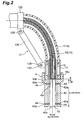
- Fig. 1 is a diagram showing the outer appearance of a light guiding device 1.
- Fig. 2 is a partial sectional view showing a region X in Fig. 1 of light guiding device 1 in enlarged manner.
- Fig. 3 is a diagram showing a light emitting end face of a light guide cable 10.
- Fig. 4 is a diagram showing a light emitting end face of an illumination head 4.
- Fig. 5 is a diagram showing the end face of a first light incidence part.
- Fig. 6 is a diagram showing the manner in which a light emitting end face side front end part of an optical fiber bundle 16 is fitted into a sleeve member 13.
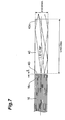
- Fig. 7 is a diagram, showing the manner in which light is totally reflected and propagated in a cross section along the length direction (cross section containing the diagonal of a light emitting end face 40o) of a glass rod 40.
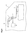
- Fig. 8 is a schematic diagram of a semiconductor wafer periphery exposure device 5 to which light guiding device 1 is applied.
- Fig. 1 is a diagram showing the outer appearance of light guiding device 1.
- Fig. 2 is a partial sectional view showing a region X in Fig. 1 of light guiding device 1 in enlarged manner.
- Light guiding device 1 is equipped, at a light emitting end face side, with a light guide cable 10, which is arranged by an optical fiber bundle 16, formed by bundling together a plurality of optical fiber cores (UV transmitting quartz fiber cores), being covered by a PVC cladding 17.
- the light guide cable 10 is branched at a light incidence end face side into a light guide cable 20 and light guide cable 30.
- Light guide cable 20 and light guide cable 30 are substantially equal in the number of cores, and by bundling together the optical fiber cores that make up these cables at the branching part, optical fiber bundle 16 of light guide cable 10 is formed.
- the branching part of this optical fiber cable is covered by a branching part outer cover 11.
- FIG. 3 is a diagram showing the light emitting end face of light guide cable 10.
- Fig. 6 is a diagram showing the manner in which the light emitting end face side front end part of optical fiber bundle 16 is fitted into sleeve member 13.
- Optical fiber bundle 16 is fixed in shape at the light emitting end face side front end part (part corresponding to a region Y shown in Fig.
- the cross-sectional shape of the light emitting end face side front end part is formed to a rectangular shape, which is 8.0mm in the lateral direction and 4.0mm in the longitudinal direction, as shown in Fig. 3 .
- the alignment of the optical fiber cores at the light emitting end face side front end part is preferably as random as possible with respect to the alignment of the optical fiber cores at the other parts. The making of the alignment of the optical fiber cores at the light emitting end face side front end part random contributes to the making uniform of the scattering of the light amounts of the light emitting from the respective optical fiber cores.
- sleeve member 13 is a cylindrical member, the overall shape of which is an elliptical column.
- the hollow part of sleeve member 13 has a rectangular cross section, which is 8.0mm in the lateral direction and 4.0mm in the longitudinal direction, and at the opening at one side, a step 13a is formed by the slight protruding of a side wall.
- the thickness of step 13a is adjusted to be of a predetermined length g.
- Optical fiber bundle 16 the light emitting end face side front end part of which is fixed by the adhesive agent, is inserted into the hollow part and thereby fitted into sleeve member 13.
- step 13a Upon fitting, step 13a latches onto a light emit end face 16o of optical fiber bundle 16 and a gap of interval g is formed between the bottom face of sleeve member 13 and light emitting end face 16o.
- optical fiber bundle 16 thus being fitted into sleeve member 13, the shape of the light emitting end face side front end part is maintained regardless of variations of the shape of optical fiber bundle 16.
- the light emitting end face side front end part being fixed by the adhesive agent, the shape is fixed even more strongly, the density of core end faces at light emitting end face 16o is made high, and dark parts (parts besides the core end faces) are lessened. The light amount density at light emitting end face 16o is thus made high.
- Sleeve member 13 is a cylindrical member, the overall shape of which is an elliptical column, and an emitting part outer cover 14, having a hollow part of elliptical columnar shape, is mounted so that the bottom face of sleeve member 13 and the bottom face of emitting part outer cover 14 are positioned on the same plane.
- the light emitting end face side front end part of optical fiber bundle 16 is covered by emitting part outer cover 14 and PVC cladding 17.
- an illumination head 4 is detachably mounted to the light emitting end face side front end part of optical fiber bundle 16.
- Illumination head 4 comprises a glass rod holding member 42, a glass rod 40, which is housed in glass rod holding member 42, and a positioning pin 44, which fixes glass rod 40, and glass rod 40 is set to oppose light emitting end face 16o of optical fiber bundle 16.
- Fig. 4 is a diagram showing a light emitting end face of illumination head 4.
- Glass rod 40 has basal faces with a rectangular shape that is 8.0mm in the lateral direction and 4.0 in the longitudinal direction and has a quadratic prism shape with a length (height) of 40.0mm.
- the basal face at one side of glass rod 40 becomes a light incidence end face 40i and the other basal face becomes a light emitting end face 40o.
- glass rod holding member 42 has a cylindrical shape and the inner periphery and outer periphery of the cross section at the front end part (glass rod housing part) are both elliptical in shape. Though the inner periphery and outer periphery of the cross section at the terminal end part (emitting part outer cover mounting part) are also elliptical, the inner peripheral diameters of the emitting part outer cover mounting part are greater than the inner peripheral diameters of the glass rod housing part.
- the major diameter of the inner periphery of the cross section is set to be longer than 8.0mm (the length of the lateral side of light emitting end face 40o of glass rod 40) and the minor diameter is set to be longer than 4.0mm (the length of the longitudinal side of light emitting end face 40o of glass rod 40).
- the length of the hollow part is set to 40.0mm (the length of glass rod 40).
- four positioning pin insertion holes 42a are formed at each of the front end part side and the terminal end part side. Glass rod 40 is housed with a degree of freedom when it is inserted into the glass rod housing part and the position of glass rod 40 is fixed by positioning pins 44 that are inserted into positioning pin insertion holes 42a. Threaded grooves may be formed at the side faces of positioning pin insertion holes 42a and positioning screws may be screwed into positioning pin insertion holes 42a in place of positioning pins 44.
- the shape and size of the inner periphery of the cross section at the emitting part outer cover mounting part are the same as those of the outer periphery of emitting part outer cover 14, and emitting part outer cover 14 is set to be fitted in the hollow part of the emitting part outer cover mounting part.
- illumination head 4 is mounted detachably to emitting part outer cover 14.
- Illumination head 4 is thus detachably mounted via illumination part outer cover 14 to sleeve member 13. Since illumination head 4 is thus made detachable, exchange and washing of glass rod 40 are facilitated.
- a step 42b is formed at the boundary part of these parts.
- this step 42b latches onto the bottom face of emitting part outer cover 14.
- glass rod 40 is inserted into the glass rod housing part, glass rod 40 is fixed so that light incidence end face 40i is positioned on the same plane as step 42b (the bottom faces of emitting part outer cover 14 and sleeve member 13).
- glass rod 40 is fixed so as to oppose light emitting end face 16o of optical fiber bundle 16 across a gap of interval g. Furthermore, by shifting the positions of positioning pins 44, the orientation of glass rod 40 is adjusted so that light incidence end face 40i can pick up the emitting light from light emitting end face 16o without leakage.
- light guide cable 10 is curved at a right angle near the front end part and this shape is held by a curving part holding member 12.
- Curving member holding part 12 is equipped and arranged with a ring 122, a ring 124, a fixing plate 126, and screws 128.
- Ring 122 is fixed at a location near the front end part of light guide cable 10.
- Ring 124 is fixed onto the outer peripheral surface of emitting part outer cover 14. That is, ring 124 is fixed to sleeve member 13 via emitting part outer cover 14.
- the respective end parts of fixing plate 126 are mounted to ring 122 and ring 124 and, after being fastened by screws 128, are fixed by an epoxy adhesive agent.
- the optical fiber cores of optical fiber bundle 16 are twisted together to provide a bend-resistant structure. For example, approximately 200 optical fiber cores are twisted together to form a sub-bundle and seven such sub-bundles are twisted together to form the optical fiber bundle.
- light guide cable 10 is thus curved at a right angle near its front end part and this shape is held by curving part holding member 12, good maintenance of the vertical illumination state of the emitting light, prevention of damage of optical fiber bundle 16 due to repeated curving, and prevention of damage due to the contacting of the front end part of light guide cable 10 with inner peripheral parts of the exposure device resulting from the front end part being in a floating state in the process of mounting the device are enabled.
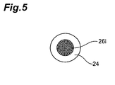
- Fig. 5 is a diagram showing the end face of the first light incidence part.
- the front end face (light incidence end face 26i) of the optical fiber bundle that makes up light guide cable 20 is exposed from incidence part outer cover 24.
- Light incidence end face 26i has a circular shape.
- Light guide cable 20 is curved near the front end part and this curved state is maintained by a curving part holding member 22.
- light guide cable 30 is equipped with a second light incidence part at its front end part and is maintained in a curved state by a curving part holding member 32.
- a light source is connected to the first light incidence part and light for exposing peripheral parts of a semiconductor wafer is taken into the optical fiber bundle from light incidence end face 26i of the first light incidence part. If an even greater amount of light is required, another light source is connected to the second light incidence part as well.
- Light from the light source is optically guided by the optical fiber bundle and emits from light emit end face 16o.
- the emitting light from light emitting end face 16o is made incident on light incidence end face 40i of glass rod 40.
- the light that is made incident on light incidence end face 40i propagates through glass rod 40 and emits from light emitting end face 40o, and in this process, the illuminance of the cross section of the emitting light is made uniform and the cross-sectional shape of the emitting light is shaped.
- Fig. 7 is a diagram, showing the manner in which light is totally reflected and propagated in the cross section along the length direction (the cross section containing the diagonal of light emitting end face 40o) of glass rod 40.
- the maximum emit angle ⁇ (maximum angle formed by the optical axis of the optical fiber cores and the emitting light) into air of the optical fiber cores that make up optical fiber bundle 16 is 11.5°.
- the length of glass rod 40 of the present embodiment is 40.0mm and satisfies the above condition. Since the emitting light from the respective optical fiber cores thus become totally reflected at the boundary of glass rod 40 and air and thereby become mixed, the non-uniformity of the illuminance at light emit end face 16o of optical fiber bundle 16 is made uniform. That is, non-uniformity of illuminance occurs at light emitting end face 16o due to such causes as the bend loss of guided light differing according to each optical fiber core, there being a clad region, in which light is not propagated, on light emitting end face 16o, etc. However, by applying glass rod 40 of the present embodiment and mixing the emitting light from the respective optical fiber cores, the non-uniformity of illuminance can be made uniform.
- light emitting end face 40o of glass rod 40 is rectangular, the cross section of the light emitting from light emitting end face 40o is shaped to a rectangular shape. There is thus no need to apply an aperture member to block the outer rim of the cross section of the emitting light to shape the light. Consequently, the light guided by the optical fiber bundle can be illuminated onto peripheral parts of a semiconductor wafer without decrease of the light amount.
- the shapes of the light emitting end face of the optical fiber bundle and the light incidence end face of the glass rod do not have to be rectangular. Even if these are not rectangular, as long as the light emitting end face of the glass rod is rectangular, the cross section of the light that emits from the light emitting end face of the glass rod will be shaped to a rectangular shape.
- Fig. 8 is a schematic diagram of a semiconductor wafer periphery exposure device 5 to which light guiding device 1 is applied.
- Semiconductor wafer periphery exposure device 5 is equipped with a casing 52, and peripheral parts (resist-removal portions) of a semiconductor wafer 6 are exposed to light inside casing 52.
- Semiconductor wafer 6 is set on a rotating supporting plate 54.
- An illumination head moving device 56 supports illumination head 4 and controls the position of illumination head 4.
- Illumination head 4 illuminates a single point of a peripheral part (resist-removal portion) of semiconductor wafer 6, and by the rotation of semiconductor wafer 6 by rotating supporting plate 54 and the movement of the illumination spot of illumination head 4 by illumination head moving device 56, peripheral parts (resist-removal portions) of semiconductor wafer 6 are exposed evenly.
- optical axis of light guide cable 10 is directed in the vertical direction at the front end part at the light emitting end face side, since the optical axis of light guide cable 10 is curved near this front end part so as to be directed in the horizontal direction, casing 52 can be made compact in size in the vertical direction. Also, the housing space at the housing position to which illumination head 4 is moved can be made small.
- a light guiding device which shapes the cross section of light, emitting from a light guide fiber, to a rectangular shape and makes uniform the illuminance across the entire cross section of the emitting light without decreasing the light amount of the emitting light, can be provided.
- the present invention can be applied, for example, to the manufacture of a semiconductor integrated circuit.
Landscapes
- Physics & Mathematics (AREA)
- General Physics & Mathematics (AREA)
- Optics & Photonics (AREA)
- Exposure Of Semiconductors, Excluding Electron Or Ion Beam Exposure (AREA)
- Optical Couplings Of Light Guides (AREA)
- Optical Fibers, Optical Fiber Cores, And Optical Fiber Bundles (AREA)
- Exposure And Positioning Against Photoresist Photosensitive Materials (AREA)
Description
- The present invention concerns a light guiding device that is used to perform exposure for removal of unnecessary resist on peripheral parts of a semiconductor wafer.
- In pattern forming processes using photolithography that are performed on semiconductor wafers, there are cases where peripheral parts of a pattern formation part are not exposed and resist remains at such peripheral parts. Since resist remaining at a peripheral part can peel off and become dust that adheres to the semiconductor wafer, it must be removed prior to entering a subsequent process. For removal of the unnecessary resist on peripheral parts of a semiconductor wafer, a method, wherein light, guided by a light guiding device, is illuminated onto a resist-removal portion and the illumination spot is moved across the resist-removal portion to expose the entire resist-removal portion, is used. With this exposure method, in order to expose the entirety of the resist-removal portion uniformly, it is required that the light emitting from the light guiding device be shaped to have a cross section of rectangular shape and that the illuminance be made uniform across the entire cross section of the emitting light.
- As a prior art of such a light guiding device, there is, for example, the light guiding device disclosed in Japanese Patent Publication Laid-open (Tokukai) No.
H10-74676 H10-74676 4,964,692 US 5,229,811 discloses a light guiding device for exposure of peripheral parts of a semiconductor wafer, comprising an optical fibre bundle.EP 0 788 032 discloses a light guiding device used for edge bead removal comprising an optical fibre bundle and an exit optical system comprising lenses. - However, with the prior-art light guiding devices, since a light blocking part of an aperture member blocks the outer rim of the light emitting from a light guiding fiber, the light amount of the emitting light is decreased.
- The present invention has been made to resolve the above issue, and an object thereof is to provide a light guiding device, which shapes the cross section of light, emitting from a light guide fiber, to a rectangular shape and makes uniform the illuminance across the entire cross section of the emitting light without decreasing the light amount of the emitting light.
- In order to achieve the above object, this invention provides in a light guiding device used for exposure of peripheral parts of a semiconductor wafer, a light guiding device, comprising: an optical fiber bundle, formed by bundling together a plurality of optical fibers and having a first light incidence end face and a first light emitting end face; a glass rod, having a second light incidence end face and a second light emitting end face and making uniform the cross section of light emitting from the second light emitting end face by taking in, from the second light incidence end face, the light emitting from the first light emitting end face of the optical fiber bundle and guiding this light to the second light emitting end face; and a glass rod holding member, which fixes the glass rod to a light emitting end face side front end part of the optical fiber bundle so that the second light incidence end face of the glass rod opposes the first light emitting end face of the optical fiber bundle; the second light emitting end face of the glass rod having a rectangular shape.
- The glass rod takes in the light emitting from the optical fiber bundle and makes the illuminance uniform across the entire cross section of the emitting light. Also, since the second light emitting end face of the glass rod has a rectangular shape, the emitting light from the glass rod is shaped to be rectangular in cross section. The light thus does not have to be shaped by applying an aperture member and blocking the outer rim of the cross section of the emitting light. Consequently, the light that is guided by the optical fiber bundle can be illuminated onto peripheral parts of a semiconductor wafer without decrease of the light amount.
- Also, with this invention's light guiding device, the glass rod preferably satisfies the relationships expressed by the following formulae (A) and (B).


L[mm]: length of the glass rod
d[mm]: length of the diagonal of the second light emitting end face of the glass rod
n: refractive index of air
n': refractive index of the glass rod
θ : maximum angle of emit from the optical fiber into air
θ' : angle of refraction of light, which has emited from the optical fiber at the maximum emit angle, upon incidence onto the second light incidence end face - When the glass rod meets the above conditions, the maximum emitted angle component, among the emitting light from the optical fiber that enters the glass rod via the central axis, is totally reflected at least once at the boundary surface (interface between the glass rod and a cladding or ambient air) of the glass rod. Thus by the total reflection and mixing of the light emitting from the respective optical fibers at the boundary surface of the glass rod, the non-uniformity of illuminance at the first light emitting end face of the optical fiber bundle is made uniform satisfactorily.
- Also, with this invention's light guiding device, it is preferable for a sleeve member, which covers the light emitting end face side front end part of the optical fiber bundle, to be equipped and for the glass rod holding member to be detachably mounted to the sleeve member.
- Since the glass rod holding member can then be removed from the sleeve member, exchange and washing of the glass rod are facilitated.
- Also, with this invention's light guiding device, it is preferable for the plurality of optical fibers to be adhered to each other by an adhesive agent at the light emitting end face side front end part of the optical fiber bundle.
- By the optical fibers being adhered by an adhesive agent at the light emitting end face side front end part of the optical fiber bundle, the shape of the light emitting end face side front end part can be maintained regardless of the shape of the optical fiber bundle. Also, the density of the core end faces at the first light emitting end face of the optical fiber bundle is made high and dark parts (parts besides the core end faces) are lessened. The light amount density at the first light emitting end face is thereby increased.
- Also with this invention's light guiding device, it is preferable for the first light emitting end face of the optical fiber bundle to oppose the second light incidence end face of the glass rod across a gap.
- By there being a gap between the second light incidence end face of the glass rod and the first light emitting end face of the optical fiber bundle, damaging of the second light incidence end face and the first light emitting end face due to contact with each other can be prevented.
- Also this invention's light guiding device is preferably equipped with a sleeve member, covering the light emitting end face side front end part of the optical fiber bundle, and a curving part holding member, which, by being fixed to the vicinity of the light emitting end face side front end part of the optical fiber bundle and to the sleeve member, maintains a state wherein the optical fiber bundle is curved in the vicinity of the front end part.
- Since the state in which the optical fiber bundle is curved in the vicinity of the light emitting end face side front end part is held by the curving part holding member of the above structure, the space occupied by the optical fiber bundle in the vicinity of the light emitting end face side front end part can be made small.
-
Fig. 1 is a diagram showing the outer appearance of a light guiding device 1. -
Fig. 2 is a partial sectional view showing a region X inFig. 1 of light guiding device 1 in enlarged manner. -
Fig. 3 is a diagram showing a light emitting end face of alight guide cable 10. -
Fig. 4 is a diagram showing a light emitting end face of anillumination head 4. -
Fig. 5 is a diagram showing the end face of a first light incidence part. -
Fig. 6 is a diagram showing the manner in which a light emitting end face side front end part of anoptical fiber bundle 16 is fitted into asleeve member 13. -
Fig. 7 is a diagram, showing the manner in which light is totally reflected and propagated in a cross section along the length direction (cross section containing the diagonal of a light emitting end face 40o) of aglass rod 40. -
Fig. 8 is a schematic diagram of a semiconductor waferperiphery exposure device 5 to which light guiding device 1 is applied. - A preferable embodiment of this invention's light guiding device shall now be described with reference to the attached drawings. In the respective drawings, the same elements shall be provided with the same symbols and redundant description shall be omitted.
- First, the structure of this embodiment's light guiding device 1 shall be described.
Fig. 1 is a diagram showing the outer appearance of light guiding device 1.Fig. 2 is a partial sectional view showing a region X inFig. 1 of light guiding device 1 in enlarged manner. Light guiding device 1 is equipped, at a light emitting end face side, with alight guide cable 10, which is arranged by anoptical fiber bundle 16, formed by bundling together a plurality of optical fiber cores (UV transmitting quartz fiber cores), being covered by a PVC cladding 17. Thelight guide cable 10 is branched at a light incidence end face side into alight guide cable 20 andlight guide cable 30.Light guide cable 20 andlight guide cable 30 are substantially equal in the number of cores, and by bundling together the optical fiber cores that make up these cables at the branching part,optical fiber bundle 16 oflight guide cable 10 is formed. The branching part of this optical fiber cable is covered by a branching partouter cover 11. - A light emitting end face side front end part of
optical fiber bundle 16 is fitted into asleeve member 13 upon adhesion of the optical fiber cores to each other by an adhesive agent in a manner such that the cross section is made rectangular in shape. The structure of the light emitting end face side front end part ofoptical fiber bundle 16 shall now be described in more detail.Fig. 3 is a diagram showing the light emitting end face oflight guide cable 10.Fig. 6 is a diagram showing the manner in which the light emitting end face side front end part ofoptical fiber bundle 16 is fitted intosleeve member 13.Optical fiber bundle 16 is fixed in shape at the light emitting end face side front end part (part corresponding to a region Y shown inFig. 6 ) by the optical fiber cores being adhered to each other by the adhesive agent. By this process, the cross-sectional shape of the light emitting end face side front end part is formed to a rectangular shape, which is 8.0mm in the lateral direction and 4.0mm in the longitudinal direction, as shown inFig. 3 . Also, the alignment of the optical fiber cores at the light emitting end face side front end part is preferably as random as possible with respect to the alignment of the optical fiber cores at the other parts. The making of the alignment of the optical fiber cores at the light emitting end face side front end part random contributes to the making uniform of the scattering of the light amounts of the light emitting from the respective optical fiber cores. - As shown in
Fig. 3 andFig. 6 ,sleeve member 13 is a cylindrical member, the overall shape of which is an elliptical column. The hollow part ofsleeve member 13 has a rectangular cross section, which is 8.0mm in the lateral direction and 4.0mm in the longitudinal direction, and at the opening at one side, astep 13a is formed by the slight protruding of a side wall. The thickness ofstep 13a is adjusted to be of a predetermined length g.Optical fiber bundle 16, the light emitting end face side front end part of which is fixed by the adhesive agent, is inserted into the hollow part and thereby fitted intosleeve member 13. Upon fitting,step 13a latches onto a light emit end face 16o ofoptical fiber bundle 16 and a gap of interval g is formed between the bottom face ofsleeve member 13 and light emitting end face 16o. Byoptical fiber bundle 16 thus being fitted intosleeve member 13, the shape of the light emitting end face side front end part is maintained regardless of variations of the shape ofoptical fiber bundle 16. Furthermore, by the light emitting end face side front end part being fixed by the adhesive agent, the shape is fixed even more strongly, the density of core end faces at light emitting end face 16o is made high, and dark parts (parts besides the core end faces) are lessened. The light amount density at light emitting end face 16o is thus made high. -
Sleeve member 13 is a cylindrical member, the overall shape of which is an elliptical column, and an emitting partouter cover 14, having a hollow part of elliptical columnar shape, is mounted so that the bottom face ofsleeve member 13 and the bottom face of emitting partouter cover 14 are positioned on the same plane. The light emitting end face side front end part ofoptical fiber bundle 16 is covered by emitting partouter cover 14 and PVC cladding 17. - As shown in
Fig. 2 , anillumination head 4 is detachably mounted to the light emitting end face side front end part ofoptical fiber bundle 16.Illumination head 4 comprises a glassrod holding member 42, aglass rod 40, which is housed in glassrod holding member 42, and apositioning pin 44, which fixesglass rod 40, andglass rod 40 is set to oppose light emitting end face 16o ofoptical fiber bundle 16. The structure ofillumination head 4 andglass rod 40 shall now be described in detail.Fig. 4 is a diagram showing a light emitting end face ofillumination head 4.Glass rod 40 has basal faces with a rectangular shape that is 8.0mm in the lateral direction and 4.0 in the longitudinal direction and has a quadratic prism shape with a length (height) of 40.0mm. The basal face at one side ofglass rod 40 becomes a lightincidence end face 40i and the other basal face becomes a light emitting end face 40o. - As shown in
Fig. 2 andFig. 4 , glassrod holding member 42 has a cylindrical shape and the inner periphery and outer periphery of the cross section at the front end part (glass rod housing part) are both elliptical in shape. Though the inner periphery and outer periphery of the cross section at the terminal end part (emitting part outer cover mounting part) are also elliptical, the inner peripheral diameters of the emitting part outer cover mounting part are greater than the inner peripheral diameters of the glass rod housing part. - At the glass rod housing part, the major diameter of the inner periphery of the cross section is set to be longer than 8.0mm (the length of the lateral side of light emitting end face 40o of glass rod 40) and the minor diameter is set to be longer than 4.0mm (the length of the longitudinal side of light emitting end face 40o of glass rod 40). Also, the length of the hollow part is set to 40.0mm (the length of glass rod 40). At the side wall of the glass rod housing part, four positioning
pin insertion holes 42a are formed at each of the front end part side and the terminal end part side.Glass rod 40 is housed with a degree of freedom when it is inserted into the glass rod housing part and the position ofglass rod 40 is fixed by positioningpins 44 that are inserted into positioningpin insertion holes 42a. Threaded grooves may be formed at the side faces of positioningpin insertion holes 42a and positioning screws may be screwed into positioningpin insertion holes 42a in place of positioning pins 44. - The shape and size of the inner periphery of the cross section at the emitting part outer cover mounting part are the same as those of the outer periphery of emitting part
outer cover 14, and emitting partouter cover 14 is set to be fitted in the hollow part of the emitting part outer cover mounting part. By the fitting of emitting partouter cover 14 in the hollow part of the emitting part outer cover mounting part,illumination head 4 is mounted detachably to emitting partouter cover 14.Illumination head 4 is thus detachably mounted via illumination partouter cover 14 tosleeve member 13. Sinceillumination head 4 is thus made detachable, exchange and washing ofglass rod 40 are facilitated. - Since the inner peripheral diameters of the emitting part outer cover mounting part are greater than the inner peripheral diameters of the glass rod housing part, a
step 42b is formed at the boundary part of these parts. When emitting partouter cover 14 is fitted in the hollow part of the emitting part outer cover mounting part, thisstep 42b latches onto the bottom face of emitting partouter cover 14. Meanwhile, whenglass rod 40 is inserted into the glass rod housing part,glass rod 40 is fixed so that lightincidence end face 40i is positioned on the same plane asstep 42b (the bottom faces of emitting partouter cover 14 and sleeve member 13). Since as mentioned above, there is a gap of interval g between the bottom face ofsleeve member 13 and light emitting end face 16o ofoptical fiber bundle 16, a gap of interval g is formed between lightincidence end face 40i ofglass rod 40 and light emitting end face 16o ofoptical fiber bundle 16. By there being a gap between lightincidence end face 40i and light emitting end face 16o, damaging of lightincidence end face 40i and light emitting end face 16o can be prevented. - As described above, when
illumination head 4 is mounted to the front end part oflight guide cable 10,glass rod 40 is fixed so as to oppose light emitting end face 16o ofoptical fiber bundle 16 across a gap of interval g. Furthermore, by shifting the positions of positioning pins 44, the orientation ofglass rod 40 is adjusted so that lightincidence end face 40i can pick up the emitting light from light emitting end face 16o without leakage. - As shown in
Fig. 1 andFig. 2 ,light guide cable 10 is curved at a right angle near the front end part and this shape is held by a curvingpart holding member 12. Curvingmember holding part 12 is equipped and arranged with aring 122, aring 124, a fixingplate 126, and screws 128.Ring 122 is fixed at a location near the front end part oflight guide cable 10.Ring 124 is fixed onto the outer peripheral surface of emitting partouter cover 14. That is,ring 124 is fixed tosleeve member 13 via emitting partouter cover 14. The respective end parts of fixingplate 126 are mounted to ring 122 andring 124 and, after being fastened byscrews 128, are fixed by an epoxy adhesive agent. Since due to the application of curvingpart holding member 12 with such an arrangement, a force acts so as to drawsleeve member 13 and a portion at the vicinity of the front end part oflight guide cable 10 towards each other, the curved state of the vicinity of the front end part oflight guide cable 10 is maintained. At the curved part, the optical fiber cores ofoptical fiber bundle 16 are twisted together to provide a bend-resistant structure. For example, approximately 200 optical fiber cores are twisted together to form a sub-bundle and seven such sub-bundles are twisted together to form the optical fiber bundle. Sincelight guide cable 10 is thus curved at a right angle near its front end part and this shape is held by curvingpart holding member 12, good maintenance of the vertical illumination state of the emitting light, prevention of damage ofoptical fiber bundle 16 due to repeated curving, and prevention of damage due to the contacting of the front end part oflight guide cable 10 with inner peripheral parts of the exposure device resulting from the front end part being in a floating state in the process of mounting the device are enabled. - At the incidence part side of light guiding device 1, the front end part of
light guide cable 20, which forms a first light incidence part, is covered by an incidence partouter cover 24.Fig. 5 is a diagram showing the end face of the first light incidence part. As shown inFig. 5 , the front end face (lightincidence end face 26i) of the optical fiber bundle that makes uplight guide cable 20 is exposed from incidence partouter cover 24. Lightincidence end face 26i has a circular shape.Light guide cable 20 is curved near the front end part and this curved state is maintained by a curvingpart holding member 22. As withlight guide cable 20,light guide cable 30 is equipped with a second light incidence part at its front end part and is maintained in a curved state by a curvingpart holding member 32. A light source is connected to the first light incidence part and light for exposing peripheral parts of a semiconductor wafer is taken into the optical fiber bundle from lightincidence end face 26i of the first light incidence part. If an even greater amount of light is required, another light source is connected to the second light incidence part as well. - The actions and effects of light guiding device 1 shall now be described. Light from the light source is optically guided by the optical fiber bundle and emits from light emit end face 16o. The emitting light from light emitting end face 16o is made incident on light
incidence end face 40i ofglass rod 40. The light that is made incident on lightincidence end face 40i propagates throughglass rod 40 and emits from light emitting end face 40o, and in this process, the illuminance of the cross section of the emitting light is made uniform and the cross-sectional shape of the emitting light is shaped. - The process by which the illuminance of the cross section of the emitting light is made uniform and the cross-sectional shape of the emitting light is shaped at
glass rod 40 shall now be described in detail.Fig. 7 is a diagram, showing the manner in which light is totally reflected and propagated in the cross section along the length direction (the cross section containing the diagonal of light emitting end face 40o) ofglass rod 40. The length d of this diagonal is 8.94mm as expressed by formula (C)
Wh: length of lateral side of light emitting end face 40o = 8.0mm
W1: length of longitudinal side of light emitting end face 40o = 4.0mm - With the present embodiment, the maximum emit angle θ (maximum angle formed by the optical axis of the optical fiber cores and the emitting light) into air of the optical fiber cores that make up
optical fiber bundle 16 is 11.5°. When light of such a maximum angle component is made incident intoglass rod 40 from lightincidence end face 40i, the angle θ' formed by the light of the maximum angle component and the optical axis (the central axis of glass rod 40) will be 7.768° as expressed by formula (D), derived from formula (B):

n: refractive index of air = 1
n': refractive index ofglass rod 40 = 1.475 - Here, the condition of the length of
glass rod 40, for making the abovementioned light of the maximum angle component (presumed to be made incident intoglass rod 4 along the central axis) be totally reflected at least once at the interface betweenglass rod 40 and air, is expressed by formula (A).
L[mm] : length of theglass rod 40 - The length of
glass rod 40 of the present embodiment is 40.0mm and satisfies the above condition. Since the emitting light from the respective optical fiber cores thus become totally reflected at the boundary ofglass rod 40 and air and thereby become mixed, the non-uniformity of the illuminance at light emit end face 16o ofoptical fiber bundle 16 is made uniform. That is, non-uniformity of illuminance occurs at light emitting end face 16o due to such causes as the bend loss of guided light differing according to each optical fiber core, there being a clad region, in which light is not propagated, on light emitting end face 16o, etc. However, by applyingglass rod 40 of the present embodiment and mixing the emitting light from the respective optical fiber cores, the non-uniformity of illuminance can be made uniform. - Also, since light emitting end face 40o of
glass rod 40 is rectangular, the cross section of the light emitting from light emitting end face 40o is shaped to a rectangular shape. There is thus no need to apply an aperture member to block the outer rim of the cross section of the emitting light to shape the light. Consequently, the light guided by the optical fiber bundle can be illuminated onto peripheral parts of a semiconductor wafer without decrease of the light amount. The shapes of the light emitting end face of the optical fiber bundle and the light incidence end face of the glass rod do not have to be rectangular. Even if these are not rectangular, as long as the light emitting end face of the glass rod is rectangular, the cross section of the light that emits from the light emitting end face of the glass rod will be shaped to a rectangular shape. -
Fig. 8 is a schematic diagram of a semiconductor waferperiphery exposure device 5 to which light guiding device 1 is applied. Semiconductor waferperiphery exposure device 5 is equipped with acasing 52, and peripheral parts (resist-removal portions) of asemiconductor wafer 6 are exposed to light insidecasing 52.Semiconductor wafer 6 is set on a rotating supportingplate 54. An illuminationhead moving device 56supports illumination head 4 and controls the position ofillumination head 4.Illumination head 4 illuminates a single point of a peripheral part (resist-removal portion) ofsemiconductor wafer 6, and by the rotation ofsemiconductor wafer 6 by rotating supportingplate 54 and the movement of the illumination spot ofillumination head 4 by illuminationhead moving device 56, peripheral parts (resist-removal portions) ofsemiconductor wafer 6 are exposed evenly. - Though the optical axis of
light guide cable 10 is directed in the vertical direction at the front end part at the light emitting end face side, since the optical axis oflight guide cable 10 is curved near this front end part so as to be directed in the horizontal direction, casing 52 can be made compact in size in the vertical direction. Also, the housing space at the housing position to whichillumination head 4 is moved can be made small. - As described above, with this invention, a light guiding device, which shapes the cross section of light, emitting from a light guide fiber, to a rectangular shape and makes uniform the illuminance across the entire cross section of the emitting light without decreasing the light amount of the emitting light, can be provided.
- The present invention can be applied, for example, to the manufacture of a semiconductor integrated circuit.
Claims (6)
- A light guiding device for exposure of peripheral parts of a semiconductor wafer, comprising:an optical fiber bundle (16), formed by bundling together a plurality of optical fibers and having a first light incidence end face and a first light emitting end face (16o); characterised in that it further comprises:a glass rod (40), having a second light incidence end face (40i) and a second light emitting end face (40o) and making uniform the cross section of light emitting from said second light emitting end face (40o) by taking in, at said second light incidence end face (40i), the light having emitted from said first light emitting end face (16o) of the optical fiber bundle and guiding this light to said second light emitting end face (40o); anda glass rod holding member (42), which fixes said glass rod (40) to a light emitting end face side front end part of said optical fiber bundle (16) so that said second light incidence end face (40i) of the glass rod faces said first light emitting end face (16o) of the optical fiber bundle,said second light emitting end face (40o) of the glass rod having a rectangular shape.
- The light guiding device according to Claim 1, wherein said glass rod satisfies the relationships expressed by the following formulae (A) and (B):


where:
L[mm] : length of said glass rod
d[mm] : length of the diagonal of said second light emitting end face of the glass rod
n : refractive index of air
n' : refractive index of said glass rod
θ : maximum emit angle from said optical fiber into air
θ' : angle of refraction of light, which has emitted from said optical fiber at the maximum emit angle, upon incidence onto said second light incidence end face. - The light guiding device according to Claim 1 or 2, comprising a sleeve member (13), which covers the light emitting end face side front end part of said optical fiber bundle, and wherein said glass rod holding member (42) is detachably mounted to said sleeve member (13).
- The light guiding device according to any of Claims 1 to 3, wherein
said plurality of optical fibers adheres to each other by an adhesive agent at the light emitting end face side front end part of said optical fiber bundle. - The light guiding device according to any of Claims 1 to 4, wherein
said first light emitting end face of the said optical fiber bundle faces said second light incidence end face (40i) of the glass rod via a gap. - The light guiding device according to any of Claims 1 to 5, comprising:a sleeve member (13), covering the light emitting end face side front end part of said optical fiber bundle; anda curving part holding member (12), which, by being fixed to a portion of said optical fiber bundle in the vicinity of the light emitting end face side front end part (16o) and to said sleeve member (13), maintains a state wherein said optical fiber bundle is curved in the vicinity of said front end part.
Applications Claiming Priority (3)
| Application Number | Priority Date | Filing Date | Title |
|---|---|---|---|
| JP2002217184 | 2002-07-25 | ||
| JP2002217184A JP4302373B2 (en) | 2002-07-25 | 2002-07-25 | Light guide device |
| PCT/JP2003/008560 WO2004012244A1 (en) | 2002-07-25 | 2003-07-04 | Light conducting device |
Publications (3)
| Publication Number | Publication Date |
|---|---|
| EP1548802A1 EP1548802A1 (en) | 2005-06-29 |
| EP1548802A4 EP1548802A4 (en) | 2007-12-19 |
| EP1548802B1 true EP1548802B1 (en) | 2008-07-30 |
Family
ID=31184599
Family Applications (1)
| Application Number | Title | Priority Date | Filing Date |
|---|---|---|---|
| EP03741212A Expired - Lifetime EP1548802B1 (en) | 2002-07-25 | 2003-07-04 | Light conducting device |
Country Status (9)
| Country | Link |
|---|---|
| US (1) | US7360953B2 (en) |
| EP (1) | EP1548802B1 (en) |
| JP (1) | JP4302373B2 (en) |
| KR (1) | KR100936591B1 (en) |
| CN (1) | CN1672242B (en) |
| AU (1) | AU2003281709A1 (en) |
| DE (1) | DE60322557D1 (en) |
| TW (1) | TWI278719B (en) |
| WO (1) | WO2004012244A1 (en) |
Families Citing this family (6)
| Publication number | Priority date | Publication date | Assignee | Title |
|---|---|---|---|---|
| JP2010014815A (en) * | 2008-07-01 | 2010-01-21 | Mitsubishi Electric Corp | Projection type display device |
| JP2010170835A (en) * | 2009-01-22 | 2010-08-05 | Sanyo Electric Co Ltd | Illuminating device and projection video display device |
| JP6061571B2 (en) * | 2012-09-04 | 2017-01-18 | キヤノン株式会社 | Subject information acquisition device |
| JP6082721B2 (en) * | 2014-10-01 | 2017-02-15 | Hoya Candeo Optronics株式会社 | Light irradiation device for peripheral exposure equipment |
| JP6002261B2 (en) * | 2015-03-11 | 2016-10-05 | Hoya Candeo Optronics株式会社 | Light irradiation device |
| CN106842828B (en) * | 2017-04-05 | 2019-09-03 | 无锡影速半导体科技有限公司 | A kind of fixed device of optical tunnel |
Family Cites Families (10)
| Publication number | Priority date | Publication date | Assignee | Title |
|---|---|---|---|---|
| US4964692A (en) * | 1982-07-21 | 1990-10-23 | Smith & Nephew Dyonics, Inc. | Fiber bundle illumination system |
| US4662714A (en) | 1983-10-28 | 1987-05-05 | Kei Mori | Integrated construction of a large number of optical conductor cables |
| US5229811A (en) * | 1990-06-15 | 1993-07-20 | Nikon Corporation | Apparatus for exposing peripheral portion of substrate |
| JP3219925B2 (en) | 1993-12-27 | 2001-10-15 | 東京エレクトロン株式会社 | Peripheral exposure apparatus and peripheral exposure method |
| JP3237522B2 (en) * | 1996-02-05 | 2001-12-10 | ウシオ電機株式会社 | Wafer peripheral exposure method and apparatus |
| JP3223826B2 (en) | 1996-06-26 | 2001-10-29 | ウシオ電機株式会社 | Unnecessary resist exposure equipment on substrate |
| JPH10233354A (en) | 1997-02-20 | 1998-09-02 | Ushio Inc | Ultraviolet radiation apparatus |
| JP3356047B2 (en) | 1997-11-26 | 2002-12-09 | ウシオ電機株式会社 | Wafer peripheral exposure equipment |
| JP2001195901A (en) * | 2000-01-14 | 2001-07-19 | Nippon Sheet Glass Co Ltd | Illumination apparatus |
| JP4090273B2 (en) * | 2002-05-23 | 2008-05-28 | 株式会社Sokudo | Edge exposure device |
-
2002
- 2002-07-25 JP JP2002217184A patent/JP4302373B2/en not_active Expired - Fee Related
-
2003
- 2003-07-04 AU AU2003281709A patent/AU2003281709A1/en not_active Abandoned
- 2003-07-04 CN CN038178184A patent/CN1672242B/en not_active Expired - Fee Related
- 2003-07-04 EP EP03741212A patent/EP1548802B1/en not_active Expired - Lifetime
- 2003-07-04 WO PCT/JP2003/008560 patent/WO2004012244A1/en active IP Right Grant
- 2003-07-04 KR KR1020047019510A patent/KR100936591B1/en not_active IP Right Cessation
- 2003-07-04 DE DE60322557T patent/DE60322557D1/en not_active Expired - Lifetime
- 2003-07-04 US US10/522,180 patent/US7360953B2/en not_active Expired - Fee Related
- 2003-07-24 TW TW092120212A patent/TWI278719B/en active
Also Published As
| Publication number | Publication date |
|---|---|
| US7360953B2 (en) | 2008-04-22 |
| CN1672242A (en) | 2005-09-21 |
| JP2004063597A (en) | 2004-02-26 |
| EP1548802A1 (en) | 2005-06-29 |
| KR100936591B1 (en) | 2010-01-13 |
| AU2003281709A1 (en) | 2004-02-16 |
| WO2004012244A1 (en) | 2004-02-05 |
| KR20050020818A (en) | 2005-03-04 |
| TWI278719B (en) | 2007-04-11 |
| TW200405123A (en) | 2004-04-01 |
| DE60322557D1 (en) | 2008-09-11 |
| CN1672242B (en) | 2010-04-21 |
| EP1548802A4 (en) | 2007-12-19 |
| JP4302373B2 (en) | 2009-07-22 |
| US20060099754A1 (en) | 2006-05-11 |
Similar Documents
| Publication | Publication Date | Title |
|---|---|---|
| US10684419B2 (en) | Waveguide connector elements and optical assemblies incorporating the same | |
| CA2245974C (en) | Metal coated optical fiber array module | |
| EP1780564B1 (en) | Optical fibre with fluorescent tip cap and methods of manufacturing | |
| EP0798579A1 (en) | Optical integrated circuit having passively aligned fibers | |
| US8485738B2 (en) | Optical fiber connector | |
| US5463708A (en) | Optical waveguide module having a waveguide affixed thereto at a first bonding strength and optical fibers affixed thereto at a second bonding strength | |
| CN102597835B (en) | For the base material of optical fiber and optic alignment and clamper and correlation technique | |
| JPH09145943A (en) | Curved optical waveguide and its manufacture | |
| KR20090050959A (en) | Optical waveguide device for touch panel and touch panel using the same | |
| EP1548802B1 (en) | Light conducting device | |
| JP2007178852A (en) | Optical wiring board and optical module using the same | |
| TWI619979B (en) | Low reflection fiber-optic connector | |
| JPH11352344A (en) | Low crosstalk optical wiring | |
| US5392368A (en) | Process for mounting an optical coupling of an optical fiber on a substrate and substrate equipped with an optical fiber | |
| JP3622800B2 (en) | Optical recording device | |
| JP2006284714A (en) | Optical monitor array and manufacturing method therefor | |
| JP4565076B2 (en) | Optical path conversion device, optical transmission device manufacturing method, and manufacturing tool therefor | |
| US20210116650A1 (en) | Optical-path-bending connector and optical-path-bending connector assembly | |
| EP2031427B1 (en) | Optical terminal | |
| KR100437063B1 (en) | Plane light source using optical fiber and method thereof | |
| JP2016212414A (en) | Waveguide coupling circuit | |
| KR20050075800A (en) | Optical cable for optical signal detection and method manufacturing it | |
| JPH10208022A (en) | Fiber optical plate | |
| JP2007071951A (en) | Optical device equipped with optical connecting means and its manufacturing method | |
| JP2003194667A (en) | Optical fiber end face inspection device |
Legal Events
| Date | Code | Title | Description |
|---|---|---|---|
| PUAI | Public reference made under article 153(3) epc to a published international application that has entered the european phase |
Free format text: ORIGINAL CODE: 0009012 |
|
| 17P | Request for examination filed |
Effective date: 20050216 |
|
| AK | Designated contracting states |
Kind code of ref document: A1 Designated state(s): AT BE BG CH CY CZ DE DK EE ES FI FR GB GR HU IE IT LI LU MC NL PT RO SE SI SK TR |
|
| AX | Request for extension of the european patent |
Extension state: AL LT LV MK |
|
| DAX | Request for extension of the european patent (deleted) | ||
| RBV | Designated contracting states (corrected) |
Designated state(s): DE FR GB IT |
|
| A4 | Supplementary search report drawn up and despatched |
Effective date: 20071120 |
|
| GRAP | Despatch of communication of intention to grant a patent |
Free format text: ORIGINAL CODE: EPIDOSNIGR1 |
|
| GRAS | Grant fee paid |
Free format text: ORIGINAL CODE: EPIDOSNIGR3 |
|
| GRAA | (expected) grant |
Free format text: ORIGINAL CODE: 0009210 |
|
| AK | Designated contracting states |
Kind code of ref document: B1 Designated state(s): DE FR GB IT |
|
| REG | Reference to a national code |
Ref country code: GB Ref legal event code: FG4D |
|
| REF | Corresponds to: |
Ref document number: 60322557 Country of ref document: DE Date of ref document: 20080911 Kind code of ref document: P |
|
| PLBE | No opposition filed within time limit |
Free format text: ORIGINAL CODE: 0009261 |
|
| STAA | Information on the status of an ep patent application or granted ep patent |
Free format text: STATUS: NO OPPOSITION FILED WITHIN TIME LIMIT |
|
| 26N | No opposition filed |
Effective date: 20090506 |
|
| PGFP | Annual fee paid to national office [announced via postgrant information from national office to epo] |
Ref country code: GB Payment date: 20120704 Year of fee payment: 10 |
|
| PGFP | Annual fee paid to national office [announced via postgrant information from national office to epo] |
Ref country code: DE Payment date: 20130626 Year of fee payment: 11 |
|
| PGFP | Annual fee paid to national office [announced via postgrant information from national office to epo] |
Ref country code: FR Payment date: 20130724 Year of fee payment: 11 |
|
| PGFP | Annual fee paid to national office [announced via postgrant information from national office to epo] |
Ref country code: IT Payment date: 20130712 Year of fee payment: 11 |
|
| GBPC | Gb: european patent ceased through non-payment of renewal fee |
Effective date: 20130704 |
|
| PG25 | Lapsed in a contracting state [announced via postgrant information from national office to epo] |
Ref country code: GB Free format text: LAPSE BECAUSE OF NON-PAYMENT OF DUE FEES Effective date: 20130704 |
|
| REG | Reference to a national code |
Ref country code: DE Ref legal event code: R119 Ref document number: 60322557 Country of ref document: DE |
|
| REG | Reference to a national code |
Ref country code: FR Ref legal event code: ST Effective date: 20150331 |
|
| PG25 | Lapsed in a contracting state [announced via postgrant information from national office to epo] |
Ref country code: DE Free format text: LAPSE BECAUSE OF NON-PAYMENT OF DUE FEES Effective date: 20150203 Ref country code: IT Free format text: LAPSE BECAUSE OF NON-PAYMENT OF DUE FEES Effective date: 20140704 |
|
| REG | Reference to a national code |
Ref country code: DE Ref legal event code: R119 Ref document number: 60322557 Country of ref document: DE Effective date: 20150203 |
|
| PG25 | Lapsed in a contracting state [announced via postgrant information from national office to epo] |
Ref country code: FR Free format text: LAPSE BECAUSE OF NON-PAYMENT OF DUE FEES Effective date: 20140731 |