EP1548746A2 - Aufzeichnungsmedium mit hoher Speicherdichte - Google Patents
Aufzeichnungsmedium mit hoher Speicherdichte Download PDFInfo
- Publication number
- EP1548746A2 EP1548746A2 EP04026058A EP04026058A EP1548746A2 EP 1548746 A2 EP1548746 A2 EP 1548746A2 EP 04026058 A EP04026058 A EP 04026058A EP 04026058 A EP04026058 A EP 04026058A EP 1548746 A2 EP1548746 A2 EP 1548746A2
- Authority
- EP
- European Patent Office
- Prior art keywords
- fullerenes
- fullerene
- bound portion
- cnt
- complex
- Prior art date
- Legal status (The legal status is an assumption and is not a legal conclusion. Google has not performed a legal analysis and makes no representation as to the accuracy of the status listed.)
- Withdrawn
Links
Images

Classifications
-
- G—PHYSICS
- G11—INFORMATION STORAGE
- G11C—STATIC STORES
- G11C13/00—Digital stores characterised by the use of storage elements not covered by groups G11C11/00, G11C23/00, or G11C25/00
- G11C13/02—Digital stores characterised by the use of storage elements not covered by groups G11C11/00, G11C23/00, or G11C25/00 using elements whose operation depends upon chemical change
- G11C13/025—Digital stores characterised by the use of storage elements not covered by groups G11C11/00, G11C23/00, or G11C25/00 using elements whose operation depends upon chemical change using fullerenes, e.g. C60, or nanotubes, e.g. carbon or silicon nanotubes
-
- B—PERFORMING OPERATIONS; TRANSPORTING
- B82—NANOTECHNOLOGY
- B82Y—SPECIFIC USES OR APPLICATIONS OF NANOSTRUCTURES; MEASUREMENT OR ANALYSIS OF NANOSTRUCTURES; MANUFACTURE OR TREATMENT OF NANOSTRUCTURES
- B82Y10/00—Nanotechnology for information processing, storage or transmission, e.g. quantum computing or single electron logic
-
- H—ELECTRICITY
- H10—SEMICONDUCTOR DEVICES; ELECTRIC SOLID-STATE DEVICES NOT OTHERWISE PROVIDED FOR
- H10K—ORGANIC ELECTRIC SOLID-STATE DEVICES
- H10K85/00—Organic materials used in the body or electrodes of devices covered by this subclass
- H10K85/20—Carbon compounds, e.g. carbon nanotubes or fullerenes
- H10K85/211—Fullerenes, e.g. C60
-
- H—ELECTRICITY
- H10—SEMICONDUCTOR DEVICES; ELECTRIC SOLID-STATE DEVICES NOT OTHERWISE PROVIDED FOR
- H10K—ORGANIC ELECTRIC SOLID-STATE DEVICES
- H10K85/00—Organic materials used in the body or electrodes of devices covered by this subclass
- H10K85/20—Carbon compounds, e.g. carbon nanotubes or fullerenes
- H10K85/221—Carbon nanotubes
-
- H—ELECTRICITY
- H10—SEMICONDUCTOR DEVICES; ELECTRIC SOLID-STATE DEVICES NOT OTHERWISE PROVIDED FOR
- H10K—ORGANIC ELECTRIC SOLID-STATE DEVICES
- H10K85/00—Organic materials used in the body or electrodes of devices covered by this subclass
- H10K85/60—Organic compounds having low molecular weight
- H10K85/615—Polycyclic condensed aromatic hydrocarbons, e.g. anthracene
Definitions
- the present invention relates to high-density recording media in which a nanoscale structural change in fullerenes contained in carbon nanotubes is utilized.
- optical disc storage media such as CD-ROMs, CD-Rs, CD-RWs, and DVDs
- magneto-optical storage media such as MOs and MDs
- CD-ROMs and DVD-ROMs pits are formed (the difference between a pit portion and a flat portion in laser light reflection is binarized).
- thermal deformation of organic pigments is utilized (the difference between a deformed portion and a non-deformed portion in laser light reflection is binarized).
- CD-RWs and DVD-RWs utilize a phase change (the difference between a crystalline portion and an amorphous portion in laser light reflection is binarized), and MOs and MDs utilize a change in magnetic domain (the difference in magnetic domain is binarized).
- the binary information in accordance with the current binarization information recording methods is of a micrometer level.
- a pit measures 0.83 ⁇ m and a pitch 1.6 ⁇ m
- a pit measures 0.64 ⁇ m and a pitch 0.74 ⁇ m.
- CNTs carbon nanotubes
- JP Patent Publication (Kokai) No. 2002-97009 A and No. 2002-97010 A disclose the inclusion of a variety of substances inside carbon nanotubes (CNTs). Specifically, they describe a hybrid monolayer carbon nanotube that includes a foreign substance, such as endohederal metallofullerene, within the space of the monolayer carbon nanotube cylinder.
- WO00/48195 A1 describes the recording of binary information based on charged transportation of fullerene in a carbon nanotube.
- the aforementioned object of the invention is achieved by a nanoscale binarization information recording technique whereby the sequence of individual fullerenes in a fullerene/carbon nanotube complex (peapod) consisting of a single-wall carbon nanotube in which fullerenes are inserted in sequence is structurally changed.
- peapod a fullerene/carbon nanotube complex
- the invention provides a high-density recording medium comprising a fullerene/carbon nanotube complex (peapod) comprising a single-wall carbon nanotube in which fullerenes are inserted in series.
- a fullerene/carbon nanotube complex peapod
- the structural difference between a locally bound portion and a non-bound portion of the series of fullerenes is recorded as binary information.
- the invention provides a method of recording binary information.
- the method comprises irradiating a fullerene/carbon nanotube complex (peapod) comprising a single-wall carbon nanotube (SWCNT) in which fullerenes are inserted in series with an energy beam while heating the complex, so that only fullerenes at specific sites can bind to each other.
- the structural difference between a locally bound portion and a non-bound portion of the series of fullerenes is recorded as binary information.
- the invention provides a method of reading binary information in a high-density recording medium comprising a fullerene/carbon nanotube complex (peapod) comprising a single-wall carbon nanotube in which fullerenes are inserted in series, wherein the structural difference between a locally bound portion and a non-bound portion of the series of fullerenes is recorded as binary information.
- the method comprises reading the structural difference between the locally bound portion and the non-bound portion on the basis of the reflectivity of an energy beam used for irradiation.
- the present invention enables the storage capacity to be increased by a factor of approximately 1000 or more in terms of pit width and approximately 100 or more in terms of pitch width, for a total factor of approximately 100,000 or more, as compared with conventional, micrometer-level binarization information recording techniques.
- Fig. 1 schematically illustrates the concept of the invention.
- a fullerene/carbon nanotube complex consisting of a single-wall carbon nanotube (SWCNT) in which fullerenes are inserted in series is prepared (preparation of a peapod: Fig. 1A).
- the complex is heated and then locally irradiated with an energy beam, such as an electron beam, so that two adjacent fullerenes bind to each other, forming a local double-wall carbon nanotube (DWCNT) (binding of fullerenes only at a specific site by localized irradiation: Fig. 1B).
- the localized irradiation must take place on the order of 1 nm, such as via an electron beam or an X-ray beam. When performed at a certain temperature, the irradiation process can be expected to produce a more stable structure and lead to an improvement of storage accuracy.
- the thus formed bound portion is defined as a digital "0" and the non-bound portion that has not been irradiated with the energy beam is defined as a digital "1,” or vice versa, such that the structural difference between the locally bound portion and non-bound portion of the fullerene sequence is recorded as binary information.
- an energy beam with a lower energy level than that of the previous energy beam is used so as to prevent the inducement of a further binding, and the structural difference between the locally bound portion and non-bound portion, namely the binary information, is read on the basis of reflectance (reading of the binding and non-bound portions in terms of binary information (0 or 1): Fig. 1 C).
- the reading may be carried out in any way as long as the difference in the state of binding of the fullerenes can be clearly ascertained with an accuracy on the order of 1 nm.
- the fullerene/carbon nanotube complex (peapod; CNT complex) used in the invention comprises a CNT tube in which a fullerene aggregate consisting mainly of C 60 is provided.
- a fullerene aggregate consisting mainly of C 60 is provided.
- Such a CNT complex can be readily manufactured or obtained. Since the fullerenes forming the fullerene aggregate are highly symmetrical in shape, a bound portion with a high uniformity of shape (such as in diameter) can be readily formed from such a fullerene aggregate.
- the CNT complex used in the invention is made up of a CNT and a plurality of fullerenes contained in or filling the CNT tube. These multiple fullerenes are disposed in series like a chain in the CNT tube, forming a fullerene aggregate.
- the phrase "disposed in series” herein refers to the condition in which the multiple fullerenes are arranged adjacent to each other, where the fullerenes may not necessarily be in contact with one another physically.
- a typical example of the fullerene complex forming the peapod structure is one substantially formed of C 60 .
- a CNT complex having a fullerene aggregate substantially formed of C 60 is preferably used.
- a CNT complex having a fullerene aggregate formed of fullerenes other than C 60 such as C 70 or C 82
- Examples of such fullerene complexes include a fullerene aggregate formed of fullerenes including C 60 and C 70 , and a fullerene aggregate consisting mainly of fullerenes other than C 60 , such as C 70 .
- Part or all of the fullerenes forming such a fullerene complex may be fullerenes containing a substance other than carbon (such as a metal atom, for example).
- fullerene refers to a spherical or nearly spherical fullerene.
- the fullerene should preferably be of C 100 or less.
- a CNT complex of the aforementioned structure can be prepared as follows, for example. First, a monolayer CNT with an empty tube interior is provided.
- the monolayer CNT may be one obtained by the conventional arc discharge method, pulse laser deposition method, or thermal decomposition method, for example, without any particular limitations.
- a terminal (tip) of the monolayer CNT is then opened.
- the terminal of the monolayer CNT can be selectively opened by heating in an oxidizing atmosphere (combustion treatment), or by subjecting it to an acid having an oxidizing property, such as nitric acid (acid treatment), or to another form of oxidizing treatment.
- the monolayer CNT with the open terminal and fullerenes are caused to coexist under predetermined conditions so that the fullerenes can be inserted in (fill) the tube of the monolayer CNT.
- the monolayer CNT with the open terminal and the fullerenes may be caused to coexist at temperature of 350 to 600°C (preferably from 400 to 500°C) for an hour or longer, and typically for 1 to 48 hours.
- the fullerenes contained in the tube are normally disposed in series to form a fullerene aggregate.
- a CNT complex is formed in this manner.
- a CNT complex may be obtained by causing a monolayer CNT whose terminal and/or wall surfaces have been damaged by irradiation with an electron beam, for example, to coexist with fullerenes.
- the monolayer CNT (outer tube) forming the CNT complex should preferably have a diameter in the range of approximately 0.8 to 2 nm.
- a monolayer CNT of such a size can be readily manufactured or obtained.
- a monolayer CNT with a diameter in the range of approximately 1 to 1.8 nm is particularly preferable.
- the fullerene (particularly C 60 ) can be easily made to fill the monolayer CNT, so that a CNT complex can be readily prepared. Further, this allows a fullerene bound portion with little defect to be produced in an electron beam irradiating step, which will be described later.
- the term "diameter" of the CNT herein refers to the value obtained with respect to the center of the thickness of the wall surface of the CNT. Such a diameter can be measured using a transmission electron microscope (TEM), for example.
- TEM transmission electron microscope
- irradiation via an energy beam such as an electron beam takes place while the CNT complex is heated.
- an energy beam such as an electron beam
- recovery from damage (defect) caused by the electron beam can be accelerated as compared with the case of using an electron beam at room temperature.
- the reaction for producing a bound portion from the fullerene aggregate is accelerated, while preventing (repairing) the damage done to the outer tube by electron beam irradiation.
- a CNT recording medium with only a few defects can be manufactured in a lower temperature range and within a shorter period of time than in the case of only supplying either thermal energy or electron beam energy.
- the temperature during electron beam irradiation may be above room temperature, such as in the range from 60 to 1000°C, for example, preferably from 80 to 700°C, and more preferably from 100 to 500°C. If the temperature during electron beam irradiation is higher than the above ranges (such as, for example, in a high temperature range exceeding 1000°C), the high temperature might produce a stronger effect of causing dispersion of carbon than the effect of facilitating recovery from the damage caused by electron beam irradiation. If that happens, manufacturing efficiency of the fullerene bound portion tends to decrease as compared with the case of electron beam irradiation within the above-mentioned temperature ranges.
- the acceleration voltage of the electron beam with which the CNT complex is irradiated may be 80 kV or higher, for example, or typically from 80 to 250 kV.
- the acceleration voltage is 100 kV or higher, or typically from 100 to 225 kV.
- the acceleration voltage is in the range from 100 to 200 kV. If the acceleration voltage is too low, the effect of producing the fullerene bound portion from the fullerene aggregate decreases. If the acceleration voltage is too high, the damage done by electron beam irradiation could possibly exceed the damage-recovery facilitating effect provided by the heating during irradiation.
- the amount of electron beam irradiation onto the CNT complex may be in the range from 10 to 2000 C/cm 2 /min, for example, preferably from 50 to 1000 C/cm 2 /min, and more preferably from 100 to 500 C/cm 2 /min. Electron beam irradiation should be carried out with the aforementioned level of irradiation for a period of approximately 5 seconds to 2 hours.
- the irradiation time is preferably in the range from 15 seconds to 1 hour, and more preferably in the range from 30 seconds to 30 minutes.
- An example of the apparatus used in irradiating the CNT complex with an electron beam is JEM-2010 manufactured by JEOL Ltd.
- the production efficiency of the fullerene bound portion and its quality can be significantly improved by adjusting the balance between thermal energy and electron beam energy that are supplied such that the individual energies combine to provide a synergistic effect.
- An example of such a preferable combination of the energy supply conditions involves a temperature in the range of approximately from 80 to 700°C, and preferably from 200 to 500°C, during electron beam irradiation, and an acceleration voltage of the electron beam used for irradiation in the range from approximately 80 to 250 kV, and preferably from 100 to 200 kV.
- the CNT with a form such that the fullerene bound portion and the non-bound portion are contained in a serial manner can be preferably produced by using an electron beam for irradiation with an acceleration voltage in the range from 80 to 150 kV, or more preferably from 100 to 130 kV, while heating the CNT complex to approximately 70 to 250°C, or more preferably 100 to 200°C.
- the electron beam density should preferably be in the range from 0.5 to 5 ⁇ 10 -11 A/cm 2 , and more preferably from 1 to 3 ⁇ 10 -11 A/cm 2 .
- a monolayer CNT complex with an average diameter of 1.5 nm was subjected to an acid treatment so as to open its tip.
- the monolayer CNT with the thus opened tip and C 60 were mixed and retained in vacuum (evacuation level: 1.0 ⁇ 10 -3 Pa) at 450°C for 24 hours.
- TEM transmission electron microscope
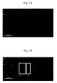
- a TEM photograph was obtained as shown in Fig. 2A revealing fullerenes C 60 filling the inside of the monolayer CNT.
- the fullerenes C 60 were disposed in series to form a fullerene aggregate. In this way, a CNT complex containing a fullerene aggregate consisting mainly of C 60 was prepared.
- the CNT complex thus prepared was then retained (pre-heated) in vacuum with an evacuation level of 1.0 ⁇ 10 -3 Pa at 400°C for an hour.
- the CNT complex was then irradiated with an electron beam with an acceleration voltage of approximately 120 kV, under the same conditions (temperature and evacuation level), for approximately 5 minutes (the amount of electron beam irradiated: approximately 200 to 250 C/cm 2 /min).
- the electron beam density was approximately 3 to 5 ⁇ 10 -11 A/cm 2 .
- the thus heated and electron-beam-irradiated product was then observed with the TEM under the aforementioned conditions. As a result, a TEM photograph was obtained, as shown in Fig. 2B, revealing a site where two fullerene molecules were bound and another site where a single fullerene molecule existed independently.
- a nanoscale high-density recording medium with a peapod structure in which fullerenes are inserted in a carbon nanotube is provided.
- the high-density recording medium of the invention has a far larger capacity than conventional recording media, and it can therefore be applied in a variety of fields.
- a high-density recording medium comprising a fullerene/carbon nanotube complex (peapod) comprising a single-wall carbon tube in which fullerenes are inserted in series.
- a structural difference between a locally bound portion and a non-bound portion of the series of fullerenes is recorded as binary information.
- the limit of storage capacity in conventional recording media based on micrometer-level binarization information recording techniques can be overcome, and a nanoscale binarization information recording technique is provided.
Landscapes
- Engineering & Computer Science (AREA)
- Chemical & Material Sciences (AREA)
- Nanotechnology (AREA)
- Physics & Mathematics (AREA)
- Mathematical Physics (AREA)
- Theoretical Computer Science (AREA)
- Crystallography & Structural Chemistry (AREA)
- Carbon And Carbon Compounds (AREA)
Applications Claiming Priority (2)
| Application Number | Priority Date | Filing Date | Title |
|---|---|---|---|
| JP2003379054A JP2005141865A (ja) | 2003-11-07 | 2003-11-07 | 高密度記録媒体 |
| JP2003379054 | 2003-11-07 |
Publications (2)
| Publication Number | Publication Date |
|---|---|
| EP1548746A2 true EP1548746A2 (de) | 2005-06-29 |
| EP1548746A3 EP1548746A3 (de) | 2005-09-21 |
Family
ID=34544479
Family Applications (1)
| Application Number | Title | Priority Date | Filing Date |
|---|---|---|---|
| EP04026058A Withdrawn EP1548746A3 (de) | 2003-11-07 | 2004-11-03 | Aufzeichnungsmedium mit hoher Speicherdichte |
Country Status (4)
| Country | Link |
|---|---|
| US (1) | US20050100500A1 (de) |
| EP (1) | EP1548746A3 (de) |
| JP (1) | JP2005141865A (de) |
| CN (1) | CN1614705A (de) |
Cited By (2)
| Publication number | Priority date | Publication date | Assignee | Title |
|---|---|---|---|---|
| CN100356607C (zh) * | 2005-10-19 | 2007-12-19 | 中国科学院上海微系统与信息技术研究所 | 一种纳米硫系化合物相变存储器的制备方法 |
| CN103170633A (zh) * | 2011-12-22 | 2013-06-26 | 中国科学院大连化学物理研究所 | 一种豆荚状碳纳米管封装非贵金属纳米颗粒的制备方法 |
Families Citing this family (4)
| Publication number | Priority date | Publication date | Assignee | Title |
|---|---|---|---|---|
| KR20160110401A (ko) * | 2014-02-03 | 2016-09-21 | 니폰 제온 가부시키가이샤 | 카본 나노튜브 섬유 및 그의 제조 방법 |
| KR20250057128A (ko) | 2015-12-30 | 2025-04-28 | 코디악 사이언시스 인코포레이티드 | 항체 및 이의 접합체 |
| EP3758737A4 (de) | 2018-03-02 | 2022-10-12 | Kodiak Sciences Inc. | Il-6-antikörper und fusionskonstrukte und konjugate davon |
| CA3157509A1 (en) | 2019-10-10 | 2021-04-15 | Kodiak Sciences Inc. | Methods of treating an eye disorder |
Family Cites Families (8)
| Publication number | Priority date | Publication date | Assignee | Title |
|---|---|---|---|---|
| JP3298735B2 (ja) * | 1994-04-28 | 2002-07-08 | 科学技術振興事業団 | フラーレン複合体 |
| ES2264928T3 (es) * | 1999-02-12 | 2007-02-01 | Board Of Trustees Operating Michigan State University | Nanocapsulas que contienen particulas cargadas, sus usos y procedimientos de preparacion de las mismas. |
| AUPR197400A0 (en) * | 2000-12-08 | 2001-01-11 | Swinburne University Of Technology | Data storage |
| GB0116943D0 (en) * | 2001-07-11 | 2001-09-05 | Isis Innovation | Information register |
| JP4306990B2 (ja) * | 2001-10-18 | 2009-08-05 | 独立行政法人産業技術総合研究所 | 非線形光学素子 |
| JP3744416B2 (ja) * | 2001-12-07 | 2006-02-08 | 日産自動車株式会社 | ブレーキ装置用摩擦材 |
| JP3849606B2 (ja) * | 2002-08-06 | 2006-11-22 | 株式会社日立製作所 | 情報記録媒体、情報記録方法、情報再生方法 |
| US20060025515A1 (en) * | 2004-07-27 | 2006-02-02 | Mainstream Engineering Corp. | Nanotube composites and methods for producing |
-
2003
- 2003-11-07 JP JP2003379054A patent/JP2005141865A/ja active Pending
-
2004
- 2004-10-27 US US10/973,338 patent/US20050100500A1/en not_active Abandoned
- 2004-11-03 EP EP04026058A patent/EP1548746A3/de not_active Withdrawn
- 2004-11-05 CN CN200410088616.5A patent/CN1614705A/zh active Pending
Cited By (3)
| Publication number | Priority date | Publication date | Assignee | Title |
|---|---|---|---|---|
| CN100356607C (zh) * | 2005-10-19 | 2007-12-19 | 中国科学院上海微系统与信息技术研究所 | 一种纳米硫系化合物相变存储器的制备方法 |
| CN103170633A (zh) * | 2011-12-22 | 2013-06-26 | 中国科学院大连化学物理研究所 | 一种豆荚状碳纳米管封装非贵金属纳米颗粒的制备方法 |
| CN103170633B (zh) * | 2011-12-22 | 2015-01-28 | 中国科学院大连化学物理研究所 | 一种豆荚状碳纳米管封装非贵金属纳米颗粒的制备方法 |
Also Published As
| Publication number | Publication date |
|---|---|
| CN1614705A (zh) | 2005-05-11 |
| JP2005141865A (ja) | 2005-06-02 |
| EP1548746A3 (de) | 2005-09-21 |
| US20050100500A1 (en) | 2005-05-12 |
Similar Documents
| Publication | Publication Date | Title |
|---|---|---|
| Nakashima et al. | DNA dissolves single-walled carbon nanotubes in water | |
| US6518189B1 (en) | Method and apparatus for high density nanostructures | |
| EP1157386B1 (de) | Nanokapseln mit geladenen teilchen, deren verwendung und verfahren zu ihrer herstellung | |
| Krauss et al. | Nano-compact disks with 400 Gbit/in 2 storage density fabricated using nanoimprint lithography and read with proximal probe | |
| Tominaga | The application of silver oxide thin films to plasmon photonic devices | |
| US20040071951A1 (en) | Ultra-high-density information storage media and methods for making the same | |
| US20080213469A1 (en) | Method and appratus for high density nanostructures | |
| US7112315B2 (en) | Molecular nanowires from single walled carbon nanotubes | |
| US20020081380A1 (en) | Highly purified single-wall carbon nanotubes and production thereof | |
| Seo et al. | Synthesis and manipulation of carbon nanotubes | |
| JP3829789B2 (ja) | 多重管カーボンナノチューブ製造方法 | |
| EP1548746A2 (de) | Aufzeichnungsmedium mit hoher Speicherdichte | |
| Teng et al. | Filled carbon-nanotube heterostructures: from synthesis to application | |
| Amama et al. | Dendrimer-templated Fe nanoparticles for the growth of single-wall carbon nanotubes by plasma-enhanced CVD | |
| US20070137786A1 (en) | Nanotube elongation | |
| US20110195277A1 (en) | High density magnetic recording medium and manufacturing method thereof | |
| Muramatsu et al. | Bright photoluminescence from the inner tubes of “peapod”‐derived double‐walled carbon nanotubes | |
| Suzuki et al. | Healing of low-energy irradiation-induced defects in single-walled carbon nanotubes at room temperature | |
| Clément et al. | Large Array of Sub‐10‐nm Single‐Grain Au Nanodots for use in Nanotechnology | |
| JP3576056B2 (ja) | 記録媒体の製造方法および記録媒体 | |
| JP4860913B2 (ja) | カーボンナノチューブ複合材料及びその製造方法、並びに、磁性材料及びその製造方法 | |
| Zhou et al. | A Two‐Step Route to Self‐Assembly of CdS Nanotubes via Electrodeposition and Dissolution | |
| Ahlskog et al. | A microdeposition technique for carbon nanotubes based on electron beam lithography | |
| EP1248745A2 (de) | Einwandige kohlenstoffnanoröhren zur wasserstoffspeicherung oder superbündelbildung | |
| Fink et al. | Molecular Nanostructures-Proceedings Of The International Winterschool On Electronic Properties Of Novel Materials |
Legal Events
| Date | Code | Title | Description |
|---|---|---|---|
| PUAI | Public reference made under article 153(3) epc to a published international application that has entered the european phase |
Free format text: ORIGINAL CODE: 0009012 |
|
| 17P | Request for examination filed |
Effective date: 20041103 |
|
| AK | Designated contracting states |
Kind code of ref document: A2 Designated state(s): AT BE BG CH CY CZ DE DK EE ES FI FR GB GR HU IE IS IT LI LU MC NL PL PT RO SE SI SK TR |
|
| AX | Request for extension of the european patent |
Extension state: AL HR LT LV MK YU |
|
| PUAL | Search report despatched |
Free format text: ORIGINAL CODE: 0009013 |
|
| RIC1 | Information provided on ipc code assigned before grant |
Ipc: 7H 01L 51/30 B Ipc: 7G 11C 13/02 A |
|
| AK | Designated contracting states |
Kind code of ref document: A3 Designated state(s): AT BE BG CH CY CZ DE DK EE ES FI FR GB GR HU IE IS IT LI LU MC NL PL PT RO SE SI SK TR |
|
| AX | Request for extension of the european patent |
Extension state: AL HR LT LV MK YU |
|
| AKX | Designation fees paid |
Designated state(s): DE FR GB |
|
| STAA | Information on the status of an ep patent application or granted ep patent |
Free format text: STATUS: THE APPLICATION HAS BEEN WITHDRAWN |
|
| 18W | Application withdrawn |
Effective date: 20061024 |