EP1548745B1 - Speicheranordnung mit schneller Leseoperation und niedrigerem Stromverbrauch sowie entsprechendes Leseverfahren - Google Patents
Speicheranordnung mit schneller Leseoperation und niedrigerem Stromverbrauch sowie entsprechendes Leseverfahren Download PDFInfo
- Publication number
- EP1548745B1 EP1548745B1 EP04106858A EP04106858A EP1548745B1 EP 1548745 B1 EP1548745 B1 EP 1548745B1 EP 04106858 A EP04106858 A EP 04106858A EP 04106858 A EP04106858 A EP 04106858A EP 1548745 B1 EP1548745 B1 EP 1548745B1
- Authority
- EP
- European Patent Office
- Prior art keywords
- voltage
- memory device
- word line
- read
- cell
- Prior art date
- Legal status (The legal status is an assumption and is not a legal conclusion. Google has not performed a legal analysis and makes no representation as to the accuracy of the status listed.)
- Expired - Lifetime
Links
- 238000000034 method Methods 0.000 title claims description 12
- 230000015654 memory Effects 0.000 claims description 43
- 230000008859 change Effects 0.000 claims description 39
- 230000003213 activating effect Effects 0.000 claims description 6
- 239000000463 material Substances 0.000 description 8
- 230000001105 regulatory effect Effects 0.000 description 8
- 230000004913 activation Effects 0.000 description 7
- 230000007704 transition Effects 0.000 description 7
- 238000010586 diagram Methods 0.000 description 5
- 238000007599 discharging Methods 0.000 description 4
- 150000004770 chalcogenides Chemical class 0.000 description 3
- 230000003071 parasitic effect Effects 0.000 description 2
- 230000003068 static effect Effects 0.000 description 2
- 230000001052 transient effect Effects 0.000 description 2
- 229910000927 Ge alloy Inorganic materials 0.000 description 1
- 229910001245 Sb alloy Inorganic materials 0.000 description 1
- 229910001215 Te alloy Inorganic materials 0.000 description 1
- 229910045601 alloy Inorganic materials 0.000 description 1
- 239000000956 alloy Substances 0.000 description 1
- 238000003491 array Methods 0.000 description 1
- 230000001413 cellular effect Effects 0.000 description 1
- 238000004891 communication Methods 0.000 description 1
- 230000009977 dual effect Effects 0.000 description 1
- 238000010438 heat treatment Methods 0.000 description 1
- 238000012986 modification Methods 0.000 description 1
- 230000004048 modification Effects 0.000 description 1
- 230000000737 periodic effect Effects 0.000 description 1
- 230000009467 reduction Effects 0.000 description 1
- 239000010409 thin film Substances 0.000 description 1
Images


Classifications
-
- G—PHYSICS
- G11—INFORMATION STORAGE
- G11C—STATIC STORES
- G11C7/00—Arrangements for writing information into, or reading information out from, a digital store
- G11C7/12—Bit line control circuits, e.g. drivers, boosters, pull-up circuits, pull-down circuits, precharging circuits, equalising circuits, for bit lines
-
- G—PHYSICS
- G11—INFORMATION STORAGE
- G11C—STATIC STORES
- G11C13/00—Digital stores characterised by the use of storage elements not covered by groups G11C11/00, G11C23/00, or G11C25/00
- G11C13/0002—Digital stores characterised by the use of storage elements not covered by groups G11C11/00, G11C23/00, or G11C25/00 using resistive RAM [RRAM] elements
- G11C13/0004—Digital stores characterised by the use of storage elements not covered by groups G11C11/00, G11C23/00, or G11C25/00 using resistive RAM [RRAM] elements comprising amorphous/crystalline phase transition cells
-
- G—PHYSICS
- G11—INFORMATION STORAGE
- G11C—STATIC STORES
- G11C13/00—Digital stores characterised by the use of storage elements not covered by groups G11C11/00, G11C23/00, or G11C25/00
- G11C13/0002—Digital stores characterised by the use of storage elements not covered by groups G11C11/00, G11C23/00, or G11C25/00 using resistive RAM [RRAM] elements
- G11C13/0021—Auxiliary circuits
- G11C13/0023—Address circuits or decoders
- G11C13/0026—Bit-line or column circuits
-
- G—PHYSICS
- G11—INFORMATION STORAGE
- G11C—STATIC STORES
- G11C13/00—Digital stores characterised by the use of storage elements not covered by groups G11C11/00, G11C23/00, or G11C25/00
- G11C13/0002—Digital stores characterised by the use of storage elements not covered by groups G11C11/00, G11C23/00, or G11C25/00 using resistive RAM [RRAM] elements
- G11C13/0021—Auxiliary circuits
- G11C13/0023—Address circuits or decoders
- G11C13/0028—Word-line or row circuits
-
- G—PHYSICS
- G11—INFORMATION STORAGE
- G11C—STATIC STORES
- G11C13/00—Digital stores characterised by the use of storage elements not covered by groups G11C11/00, G11C23/00, or G11C25/00
- G11C13/0002—Digital stores characterised by the use of storage elements not covered by groups G11C11/00, G11C23/00, or G11C25/00 using resistive RAM [RRAM] elements
- G11C13/0021—Auxiliary circuits
- G11C13/003—Cell access
-
- G—PHYSICS
- G11—INFORMATION STORAGE
- G11C—STATIC STORES
- G11C13/00—Digital stores characterised by the use of storage elements not covered by groups G11C11/00, G11C23/00, or G11C25/00
- G11C13/0002—Digital stores characterised by the use of storage elements not covered by groups G11C11/00, G11C23/00, or G11C25/00 using resistive RAM [RRAM] elements
- G11C13/0021—Auxiliary circuits
- G11C13/004—Reading or sensing circuits or methods
-
- G—PHYSICS
- G11—INFORMATION STORAGE
- G11C—STATIC STORES
- G11C8/00—Arrangements for selecting an address in a digital store
- G11C8/08—Word line control circuits, e.g. drivers, boosters, pull-up circuits, pull-down circuits, precharging circuits, for word lines
-
- G—PHYSICS
- G11—INFORMATION STORAGE
- G11C—STATIC STORES
- G11C13/00—Digital stores characterised by the use of storage elements not covered by groups G11C11/00, G11C23/00, or G11C25/00
- G11C13/0002—Digital stores characterised by the use of storage elements not covered by groups G11C11/00, G11C23/00, or G11C25/00 using resistive RAM [RRAM] elements
- G11C13/0021—Auxiliary circuits
- G11C13/0038—Power supply circuits
-
- G—PHYSICS
- G11—INFORMATION STORAGE
- G11C—STATIC STORES
- G11C13/00—Digital stores characterised by the use of storage elements not covered by groups G11C11/00, G11C23/00, or G11C25/00
- G11C13/0002—Digital stores characterised by the use of storage elements not covered by groups G11C11/00, G11C23/00, or G11C25/00 using resistive RAM [RRAM] elements
- G11C13/0021—Auxiliary circuits
- G11C13/0069—Writing or programming circuits or methods
- G11C2013/0071—Write using write potential applied to access device gate
-
- G—PHYSICS
- G11—INFORMATION STORAGE
- G11C—STATIC STORES
- G11C2213/00—Indexing scheme relating to G11C13/00 for features not covered by this group
- G11C2213/10—Resistive cells; Technology aspects
- G11C2213/15—Current-voltage curve
-
- G—PHYSICS
- G11—INFORMATION STORAGE
- G11C—STATIC STORES
- G11C2213/00—Indexing scheme relating to G11C13/00 for features not covered by this group
- G11C2213/70—Resistive array aspects
- G11C2213/79—Array wherein the access device being a transistor
Definitions
- the present invention relates to a fast reading, low consumption memory device and to a reading method thereof.
- the invention is particularly suited for phase change memories (PCM), although it may be advantageously exploited for other kinds of memories as well.
- PCM phase change memories
- phase change memory elements exploit the characteristics of materials which have the property of changing between two phases having distinct electrical characteristics. For example, these materials may change from an amorphous phase, which is disorderly, to a crystalline or polycrystalline phase, which is orderly, and the two phases are associated to considerably different resistivities.
- alloys of elements of group VI of the periodic table such as Te or Se, referred to as chalcogenides or chalcogenic materials, can advantageously be used in phase change cells.
- the chalcogenide that currently offers the most promise is formed by a Ge, Sb and Te alloy (Ge 2 Sb 2 Te 5 ), which is currently widely used for storing information in overwritable disks.
- the resistivity varies by two or more magnitude orders when the material passes from the amorphous phase (more resistive) to the polycrystalline phase (more conductive) and vice versa.
- PCM elements for forming memory cells and arrays has already been proposed.
- a thin film of chalcogenic material is employed as a programmable resistor, which can be electrically heated by a controlled current so as to be switched between a high and a low resistance condition.
- the state of the chalcogenic material may be read applying a sufficiently small voltage so as not to cause a sensible heating and measuring the current passing through it. Since the current is proportional to the conductance of the chalcogenic material, it is possible to discriminate between the two states.
- each PCM cell is generally associated to a selection element, normally a PNP bipolar transistor.
- each PCM cell is connected between a respective bit line and the emitter terminal of the PNP bipolar transistor forming the respective selection element. The selection element is turned on when the corresponding PCM cell is to be read and is turned off otherwise.
- a PCM cell is selected by grounding the base terminal of the corresponding selection element and by biasing the corresponding bit line at a regulated reference voltage; on the contrary, the voltage on the base terminal of a selection element is raised, and the corresponding bit line is left floating or driven to a relatively lower voltage, in order to turn off the selection element and to deselect the corresponding PCM cell.
- bit line voltage regulating elements are transistors receiving a reference voltage on their control terminals and having different conductivity with respect to the decoding transistors (normally, NMOS transistors instead of PMOS transistors); natural transistors are preferred and often required to meet low supply voltage requirements, which are becoming more and more important.
- the bit lines of the whole memory array or at least the bit lines of an addressed sector of the memory array must be fully discharged before reading.
- the selecting elements maintain one terminal of the selected PCM cell at around the ground voltage during reading, whereas the other terminal is at the voltage of the corresponding bit line.
- the voltage on the deselected bit lines is rather high, on account of the leakage currents, so that selecting a PCM cell without discharging the corresponding bit line could easily cause undesired phase transitions.
- bit line voltage regulating elements Even in the case that the bit line voltage regulating elements comprise standard transistors, in fact, their threshold voltages are sensitive to temperature variations. In other words, the bias voltage provided to the bit lines may be unstable under certain conditions.
- US 2003/026134 A1 describes a method for reading a structural phase change memory, whereby a precharge pulse is applied to raise a bit line voltage on a bit line corresponding to a selected cell, without raising cell voltage and cell current to programming levels. Then, the cell current is raised to a read level which is below the programming threshold level, and the bit line voltage is compared to a reference voltage while the cell current is at the read level.
- the aim of the present invention is to provide a memory device and a reading method thereof which are free from the above described drawbacks.
- phase change memory devices Although, reference will be made to phase change memory devices; however, the invention could be advantageously exploited for other kinds of memories as well, such as ferroelectric memories.
- a phase change memory device 1 comprises an array 2 of PCM cells 3, arranged in rows and columns and schematically illustrated by symbols of variable resistors, a column decoder 4, a row decoder 5, a row driver stage 6, a read/write voltage generating circuit 7 (which will be hereinafter referred to as R/W generator 7), a charge control circuit 8, a supply line 9, and a control unit 10.
- the supply line is connected to an external DC power source 11 for providing a supply voltage V DD to the phase change memory device 1.
- the power source 11 is a common power supply device for supplying also other devices of a system (not shown in figure 1 ) wherein the phase change memory device 1 is included.
- the PCM cells 3 of the array 2 have a current-voltage characteristic as illustrated in figure 2 , where a low resistance state and a high resistance state are indicated with LR and HR, respectively.
- Figure 2 further shows a phase change voltage V PHC , corresponding to transitions from the high resistance state HR to the low resistance state LR, and a hold voltage V H , which is not to be exceeded in order to prevent accidental phase transitions.
- PCM cells 3 arranged on the same column have respective first terminals 3a connected to a same common bit line 12; PCM cells 3 arranged on a same row have respective second terminals 3b coupled to a same word line 13 through respective selection transistor 15, in particular PNP bipolar transistors.
- second terminals 3b of the PCM cells 3 are selectively connectable to the corresponding word lines 13. More precisely, each of the selection transistors 15 has collector terminal grounded and emitter terminal connected to the second terminal 3b of the respective PCM cell 3; moreover, selection transistors 15 associated to PCM cells 3 arranged on a same row have respective base terminals connected to the same word line 13.
- the column decoder 4 is configured to selectively connect one of the bit lines 12 to the supply line 9.
- the row driver stage 6 is connected between the row decoder 5 and the array 2.
- the row decoder 5 and the row driver stage 6 are mutually connected through a plurality of row select lines 17, each corresponding to a respective word line 13 of the array 2.
- the row decoder 5 is configured to selectively activate one of the row select lines 17, thereby selecting the corresponding word line 13.
- the row driver stage 6 is connected to the R/W generator 7 through a read bias line 18 and a deselect bias line 19, for receiving a read voltage V RD and a deselect voltage V SB , respectively; and the control unit 10 supplies the row driver stage 6 with a read/write signal R/W, having a read logic level and a write logic level.
- the row driver stage 6 supplies the read voltage V RD to a word line 13 selected by the row decoder 5, and the deselect voltage V SB to the other word lines 13 of the array 2.
- the R/W generator 7 is per se known and is based, for example, on regulated charge pump circuits (here not shown).
- the charge control circuit 8 is connected to the bit lines 12 of the array 2 and receives a charge control activation signal S Q from the control unit 10.
- a charge control activation signal S Q which is a logic signal
- the charge control circuit 8 controllably discharges the bit lines 12 to a predetermined charge control voltage V x (as will be explained later on, according to the present embodiment, the bit lines tend to be charged to the deselect voltage V SB when the charge control circuit 8 is deactivated).
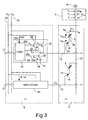
- Figure 3 shows in greater detail a PCM cell 3 selected for reading by the corresponding selection transistor 15, bit line 12, and word line 13; moreover, in figure 3 a portion of the row driver stage 6 coupled to the selected PCM cell 3 is illustrated and the column decoder 4 is only schematically sketched.
- the bit line 12 coupled to the selected PCM cell 3 is connected to the supply line 9 through the column decoder 4, which is a three level PMOS decoder in the embodiment herein described.
- the column decoder 4 comprises a plurality of first level transistors 20, a plurality of second level transistors 21 and a plurality of third level transistors 22, all of a same type, in particular, of PMOS type; for the sake of simplicity, figure 3 shows only one first level transistor 20, one second level transistor 21 and one third level transistor 22, which are involved in selecting the bit line 12 coupled to the PCM cell 3 to be read.
- the bit line 12 is directly connected to the respective first level transistor 20.
- gate terminals of the first, second and third level transistors 20-22 receive respective address signals Y1, Y2, Y3 from an external address bus of a known type and not shown herein.
- the row driver stage 6 comprises a plurality of bias circuits 24, each coupled to a respective word line 13 ( figure 3 illustrates in detail only the bias circuit 24 involved in selecting the word line 13 connected to the PCM cell 3 to be read).
- each of the bias circuit 24 comprises a respective logic circuit 25 and a respective switching circuit 26, controlled by the logic circuit 25.
- the logic circuit 25 has a row select input, connected to a respective row select line 17 from the row decoder 5, and a R/W input 25a, receiving the read/write signal R/W from the control unit 10.
- a first, a second and a third voltage select output 25b, 25c, 25d of the logic circuit 25 are connected to the switching circuit 26 and supply a first, a second and a third voltage select signal S V1 , S V2 , S V3 , respectively.
- the switching circuit 26 comprises a read switch 28, a deselect switch 29, and a write switch 30.
- the read switch 28 and the deselect switch 29 are formed by PMOS transistors having gate terminals respectively connected to the first and second outputs 25b, 25c of the logic circuit 25, source terminals respectively connected to the read bias line 18 and to the deselect bias line 19, and common drain terminals connected to the corresponding word line 13;
- the write switch 30 is formed by a NMOS transistor having gate terminal connected to the third output 25d of the logic circuit 25, source terminal grounded and drain terminal connected to the corresponding word line 13.
- a ground line 33 is used as a write bias line.
- the logic circuit 25 is configured so as to turn on one of the switches 28-30 and to deactivate the others, depending on the activation state of the corresponding row select line 17 and the read/write signal R/W.
- the logic circuit 25 turns on the deselect switch 29, thereby providing the deselect voltage V SB to the corresponding word line 13 (which is deselected).
- the logic circuit 25 alternatively turns on the read switch 28 or the write switch 30, depending on the read/write signal R/W being set at the read logic level or at the write logic level, respectively.
- the selected word line 13 is biased at appropriate voltage either for reading (word line read voltage V WL ) or writing (ground). Due to a voltage drop V SW across the source and drain terminals of the read switch 28 of the bias circuit 24, in a reading configuration of the phase change memory device 1 a word line read voltage V WL on the selected word line 13 is slightly higher than the read bias voltage V RD .
- the bit lines 12 tend to be charged at the deselect voltage V SB , on account of leakage currents flowing through the selection transistors 15.
- the phase change memory device 1 is configured for reading upon receipt of a read request.
- the control unit 10 sets the read/write signal R/W at the read logic level and the charge control activation signal S Q at the activation value, so that the charge control circuit 8 drives the bit lines 12 to the charge control voltage V x .
- the column decoder 4 selects one of the bit lines 12 corresponding to a PCM cell 3 to be read, for connection to the supply line 9; accordingly, the selected bit line 12 and the first terminals 3a of the PCM cells 3 connected thereto, in particular the selected PCM cell 3, are biased substantially at the supply voltage V DD .
- a bit line voltage V BL on the selected bit line 12 is slightly lower than the supply voltage V DD , owing to a small voltage drop V CD across the active first, second and third level transistors 20-22 of the column decoder 4.
- the row driver stage 6 supplies the read bias voltage V RD to a word line 13 selected by the row decoder 5 and corresponding to the PCM cell 3 to be read, and the deselect bias voltage V SB to the other word lines 13 of the array 2.
- a cell current I CELL flows through the selected PCM cell 3 and the respective selection transistor 15; the value of the cell current I CELL is determined by the state of the chalcogenic material of the PCM cell 3.
- the read bias voltage V RD and the word line read voltage V WL are non-zero (positive) voltages such that a suitable cell voltage V CELL drops across the selected PCM cell 3 and phase transition are prevented.
- the cell voltage V CELL is lower than the phase change voltage V PHC , and preferably lower also than the hold voltage V H .
- V BE is a conduction base-emitter voltage of the selection transistors 15.
- the charge control voltage V x is a non-zero (positive) voltage and has to be as low as required to keep in cut-off condition the selection transistors 15 coupled to deselected bit lines 12.
- the charge control voltage V x is a positive voltage complying also with the following condition: V X ⁇ V RD + V BE + V SW or V X ⁇ V WL + V BE (according to the above example, V X ⁇ 3 V). Since the voltage on the bit lines 12 is initially close to the deselect voltage V SB , the charge control transistors 32 are on, so that charge is drawn from the bit lines 12.
- the charge control activating circuit 31 selectively activates the charge control transistors 32, so that the bit lines 12 are controllably discharged only to the charge control voltage V x , before reading.
- the bit lines may be controllably discharged to a pre-determined non-zero voltage, instead of being grounded (i.e. completely discharged). Accordingly, on the one side, parasitic power consumption is significantly reduced (up to 80%), since only a small amount of charge is removed before each reading operation (and later restored by the leakage currents); of course, the greater is the charge control voltage V x , the greater is the reduction in power consumption. On the other side, the discharge transient is shorter, so that the bit lines are soon ready for reading and the reading operation is faster. Moreover, since the selected bit line is biased close to the supply voltage directly through the column decoder, a dedicated voltage regulator is no longer required. Hence, bias voltage supplied to the bit lines is stable and the need for natural transistors is overcome also in the case of low supply voltage devices.
- the phase change memory device according to the invention is simpler and cheaper to produce, compared to known memories.
- a phase change memory device 100 comprises the array 2 of PCM cells 3, the column decoder 4, the row decoder 5, the row driver stage 6, the R/W generator 7), the charge control circuit 8 and the control unit 10.
- the phase change memory device 100 further includes a charge pump 101, a voltage regulator 102 and an internal supply line 109.
- the charge pump 101 is connected to an external power source 111, for receiving an external supply voltage Vpp, and to the voltage regulator 102.
- the column decoder 4 is connected to the voltage regulator 102 over the internal supply line 109.
- the charge pump 101 co-operates with the voltage regulator 102 for supplying a regulated boosted voltage V BOOST on the internal supply line 109.
- the read bias voltage V RD and the word line read voltage V WL are non-zero (positive) voltages such that a suitable cell voltage V CELL drops across the selected PCM cell 3 and phase transition are prevented.
- the word line read voltage V WL is 4.85 V and the read bias voltage V RD is 4.75 V.
- the charge control voltage V x is determined according to equation (6), hence V x ⁇ 5.55 V.
- a phase change memory device 1' has a dual structure with respect to the phase change memory device 1 of figure 1 .
- the phase change memory device 1' comprises the array 2 of PCM cells 3, a column decoder 4', a R/W generator 7', a charge control circuit 8', and selecting transistors 15', coupled to respective PCM cells 3.
- the phase change memory device 1' includes a negative voltage supply line 9' connectable to an external power source 11' providing a negative supply voltage Vss.
- the selecting transistors 15' are NPN bipolar transistors, having emitter terminals connected to respective PCM cells 3, drain terminals connected to the supply line 9', and base terminals connected to respective word lines 13.
- the column decoder 4' is a three level NMOS decoder comprising first, second and third level transistors 20', 21', 22', and is configured for selectively connecting a bit line 12 to the negative voltage supply line 9'.
- the R/W generator 7' provides a read bias voltage V RD ' and a write bias voltage V WR on a read bias line 18' and on a write bias line 19', respectively; in this case, the ground line 33 is used as a deselect bias line.
- a read switch 28' and a write switch 29' are formed by PMOS transistors coupled to the read bias line 18' and, respectively, to the write bias line 19'; and a deselect switch 30' is formed by a NMOS transistor having a source terminal grounded. Due to a voltage drop V SW ' across the source and drain terminals of the read switch 28' of the bias circuit 24, in a reading configuration of the phase change memory device 1' a word line read voltage V WL ' on the selected word line 13 is slightly lower than the read bias voltage V RD ' (however, the absolute value of the word line read voltage V WL ' is greater than the absolute value of the read bias voltage V RD '). The read bias voltage V RD ' and the word line read voltage V WL ' are non-zero (negative) voltages such that a suitable cell voltage V CELL drops across the selected PCM cell 3 and phase transition are prevented.
- the charge control circuit 8' is connected to the bit lines 12 and is configured to controllably charge the bit lines 12 at a predetermined charge control voltage V x '.
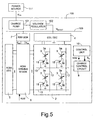
- System 200 may be used in wireless devices such as, for example, a personal digital assistant (PDA), a laptop or portable computer with wireless capability, a web tablet, a wireless telephone, a pager, an instant messaging device, a digital music player, a digital camera, or other devices that may be adapted to transmit and/or receive information wirelessly.
- PDA personal digital assistant
- System 200 may be used in any of the following systems: a wireless local area network (WLAN) system, a wireless personal area network (WPAN) system, or a cellular network, although the scope of the present invention is not limited in this respect.
- WLAN wireless local area network
- WPAN wireless personal area network
- cellular network although the scope of the present invention is not limited in this respect.
- System 200 may include a controller 210, an input/output (I/O) device 220 (e.g. a keypad, display), the phase change memory device 1, a wireless interface 240, and a static random access memory (SRAM) 260 and coupled to each other via a bus 250.
- the system 200 further includes the power source 11, which supplies power to the controller 210, the I/O device 220, the phase change memory device 1, the wireless interface 240 and the static random access memory 260.
- the power source 11 includes a battery in one embodiment. It should be noted that the scope of the present invention is not limited to embodiments having any or all of these components.
- Controller 210 may comprise, for example, one or more microprocessors, digital signal processors, micro-controllers, or the like.
- the phase change memory device 1 may be used to store messages transmitted to or by system 200.
- the phase change memory device 1 may also optionally be used to store instructions that are executed by controller 210 during the operation of system 200, and may be used to store user data.
- the instructions may be stored as digital information and the user data, as disclosed herein, may be stored in one section of the memory as digital data and in another section as analog memory. As another example, a given section at one time may be labeled as such and store digital information, and then later may be relabeled and reconfigured to store analog information.
- the I/O device 220 may be used to generate a message.
- the system 200 may use the wireless interface 240 to transmit and receive messages to and from a wireless communication network with a radio frequency (RF) signal.
- RF radio frequency
- Examples of the wireless interface 240 may include an antenna, or a wireless transceiver, such as a dipole antenna, although the scope of the present invention is not limited in this respect.
- the I/O device 220 may deliver a voltage reflecting what is stored as either a digital output (if digital information was stored), or as analog information (if analog information was stored).
- the memory device could be of a different type as well, in particular a ferroelectric memory device.
- the column decoder may have different structure, in particular a different number of decoding levels.
- the bias circuits 24 may have different structure. Read voltages and deselect voltages may be provided by an external source, instead of being generated by the internal R/W generator 7. Control signals may be supplied by an external control unit as well.
- the array 2 may be divided in sectors which are selectively activated. In this case, each sector is provided with a charge control circuit or, alternatively, an addressable charge control circuit is selectively coupled only to the bit lines of the sector to be read.
Landscapes
- Chemical & Material Sciences (AREA)
- Crystallography & Structural Chemistry (AREA)
- Engineering & Computer Science (AREA)
- Microelectronics & Electronic Packaging (AREA)
- Semiconductor Memories (AREA)
- Read Only Memory (AREA)
Claims (20)
- Phasenänderungsspeicherbauelement mit einer Lesekonfiguration, das Folgendes umfasst:mehrere in Reihen und Spalten angeordnete Speicherzellen (3), wobei jeweilige erste Anschlüsse (3a) von in derselben Spalte angeordneten Speicherzellen (3) mit derselben Bitleitung (12) verbunden sind und jeweilige zweite Anschlüsse (3b) von in derselben Reihe angeordneten Speicherzellen (3) mit derselben Wortleitung (13) verbunden sind;eine Speiseleitung (9; 109; 9'), die eine Speisespannung (VDD; VBOOST; VSS) zuführt;eine Spaltenadressierschaltung (4; 4') und eine Reihenadressierschaltung (5) zum jeweiligen Adressieren einer Bitleitung (12) und einer Wortleitung (13) entsprechend einer zum Lesen in der genannten Lesekonfiguration selektierten Speicherzelle (3);dadurch gekennzeichnet, dass die genannte Spaltenadressierschaltung (4; 4') so konfiguriert ist, dass sie die genannte adressierte Bitleitung (12) entsprechend der genannten selektierten Speicherzelle (3) im Wesentlichen mit der genannten Speisespannung (VDD; VBOOST; VSS) in der genannten Lesekonfiguration vorspannt, und dadurch, dass das Speicherbauelement eine Reihenansteuerungsschaltung (6) zum Vorspannen der genannten adressierten Wortleitung (13) entsprechend der genannten selektierten Speicherzelle (3) mit einer Wortleitungslesespannung (VWL; VWL') von ungleich null aufweist, so dass eine vorbestimmte Zellenspannung (VCELL), die niedriger ist als eine Phasenänderungsspannung (VPHC), zwischen den genannten ersten Anschluss (3a) und den genannten zweiten Anschluss (3b) der genannten selektierten Speicherzelle (3) in der genannten Lesekonfiguration angelegt wird.
- Speicherbauelement nach Anspruch 1, wobei die genannte Spaltenadressierschaltung (4) mehrere Adressierelemente (20-22; 20'-22') umfasst, alle vom selben Typ, und die genannte adressierte Bitleitung (12), die der zu leseneden Speicherzelle (3) entspricht, direkt mit einem jeweiligen genannten Adressierelement (20; 20') verbunden ist.
- Speicherbauelement nach Anspruch 1 oder 2, wobei die genannte Reihenansteuerungsschaltung (6) mehrere Vorspannungsschaltungen (24) umfasst, die mit jeweiligen Wortleitungen (13) gekoppelt sind, um selektiv eine Lesevorspannung (VRD) an die genannte adressierte Wortleitung (13) und eine Deselektiervorspannung (VSB) an die anderen Wortleitungen (13) anzulegen.
- Speicherbauelement nach einem der vorherigen Ansprüche, die eine mit den genannten Bitleitungen (12) gekoppelte Ladungsregelschaltung (8; 8') umfasst, um die genannten Bitleitungen regelbar auf eine vorbestimmte Ladungsregelspannung (VX; VX') anzusteuern, wobei die genannte Ladungsregelspannung (VX; VX') eine Nicht-Null-Spannung mit einem Absolutwert ist, der geringer ist als ein Absolutwert der genannten Wortleitungslesespannung (VWL; VWL').
- Speicherbauelement nach Anspruch 4, wobei die genannte Ladungsregelschaltung (8) mehrere Ladungsziehelemente (32), die jeweils mit einer jeweiligen Bitleitung (12) gekoppelt sind, und eine Aktivierungsschaltung (31) zum selektiven Aktivieren der genannten Ladungsziehelemente (32) umfasst.
- Speicherbauelement nach einem der vorherigen Ansprüche, das mehrere Selektierelemente (15; 15') umfasst, die jeweils mit einer jeweiligen Speicherzelle (3) gekoppelt sind.
- Speicherbauelement nach Anspruch 6, wobei jedes der genannten Selektierelemente (15; 15') einen mit einer jeweiligen Wortleitung (12) verbundenen Steueranschluss und einen mit der jeweiligen Speicherzelle (3) verbundenen Leitungsanschluss hat.
- Speicherbauelement nach Anspruch 7, wobei die genannten Selektierelemente (15) bipolare PNP-Transistoren sind.
- Speicherbauelement nach Anspruch 8, wie an Anspruch 4 angehängt, wobei die genannte Ladungsregelspannung (VX) eine positive Spannung ist, und

wobei VX die genannte Ladungsregelspannung, VWL eine Wortleitungsspannung auf der genannten selektierten Wortleitung (13) und VBE eine Basis-Emitter-Leitungsspannung des genannten, mit der genannten zu lesenden selektierten Speicherzelle (3) gekoppelten Selektierelement (15) sind. - Speicherbauelement nach einem der vorherigen Ansprüche, wobei die genannten Speicherzellen (3) Phasenänderungsspeicherzellen sind.
- Speicherbauelement nach einem der vorherigen Ansprüche, wobei die genannte Speiseleitung (9; 9') mit einer externen Stromquelle (11; 11') verbunden werden kann, um die genannte Speisespannung (VDD; VSS) zu empfangen.
- Speicherbauelement nach einem der Ansprüche 1-10, das ferner eine Spannungshochtreibschaltung (101, 102) umfasst, die mit einer externen Stromquelle (111) verbunden werden kann, um eine externe Spannung (VPP) zu empfangen und die genannte Speisespannung (VBOOST) anzulegen, wobei die genannte Speisespannung (VBOOST) eine überhöhte Spannung ist, die höher ist als die genannte externe Spannung (VPP).
- System (200), das Folgendes umfasst:eine Verarbeitungseinheit (210);eine mit der genannten Verarbeitungseinheit gekoppelte Schnittstelle (240); undein nichtflüchtiges Phasenänderungsspeicherbauelement (1; 100; 1') nach einem der vorherigen Ansprüche, das mit der genannten Verarbeitungseinheit gekoppelt ist.
- System nach Anspruch 13, wobei die genannte Schnittstelle (240) eine drahtlose Schnittstelle ist.
- Verfahren zum Lesen eines Phasenänderungsspeicherbauelementes (1; 100; 1') mit mehreren in Reihen und Spalten angeordneten Speicherzellen (3), wobei jeweilige erste Anschlüsse (3a) von in derselben Spalte angeordneten Speicherzellen (3) mit derselben Bitleitung (12) verbunden sind und jeweilige zweite Anschlüsse (3b) von in derselben Reihe angeordneten Speicherzellen (3) mit derselben Wortleitung (13) verbunden sind;
wobei das Verfahren die folgenden Schritte beinhaltet:Zuführen einer konstanten Speisespannung (VDD; VBOOST; VSS);Adressieren einer Bitleitung (12) und einer Wortleitung (13) zum Selektieren einer zu lesenden Speicherzelle (3);dadurch gekennzeichnet, dass der genannte Schritt des Adressierens einer Bitleitung (12) und einer Wortleitung das Vorspannen der genannten adressierten Bitleitung (12) entsprechend der selektierten Speicherzelle (3) im Wesentlichen mit der genannten Speisespannung (VDD; VBOOST; VSS) und das Vorspannen der genannten adressierten Wortleitung (13) entsprechend der genannten selektierten Speicherzelle (3) mit einer Wortleitungslesespannung (VWL; VWL') von ungleich null umfasst, so dass eine vorbestimmte Zellenspannung (VCELL), die niedriger ist als eine Phasenänderungsspannung (VPHC), zwischen den genannten ersten Anschluss (3a) und den genannten zweiten Anschluss (3b) der genannten selektierten Speicherzelle (3) angelegt wird. - Verfahren nach Anspruch 15, wobei die genannten Bitleitungen (12) vor dem genannten Schritt des Adressierens einer Bitleitung (12) und einer Wortleitung (13) regelbar auf eine vorbestimmte Ladungsregelspannung (VX; VX') angesteuert werden.
- Verfahren nach Anspruch 16, wobei die genannte Ladungsregelspannung (VX) eine positive Spannung ist.
- Verfahren nach einem der Ansprüche 15-17, wobei die genannten Speicherzellen (3) Phasenänderungsspeicherzellen sind.
- Verfahren nach einem der Ansprüche 15-18, wobei die genannte Speisespannung (VDD; VSS) von einer externen Stromquelle (11; 11') bereitgestellt wird.
- Verfahren nach einem der Ansprüche 15-18, wobei der genannte Schritt des Zuführens einer konstanten Speisespannung (VDD; VBOOST; VSS) ferner die Schritte des Empfangens einer externen Spannung (VPP) und des Hochtreibens der genannten externen Spannung (VPP) beinhaltet, und wobei die genannte Speisespannung (VBOOST) eine überhöhte Spannung ist, die höher ist als die genannte externe Spannung (VPP).
Priority Applications (1)
| Application Number | Priority Date | Filing Date | Title |
|---|---|---|---|
| EP04106858A EP1548745B1 (de) | 2003-12-23 | 2004-12-22 | Speicheranordnung mit schneller Leseoperation und niedrigerem Stromverbrauch sowie entsprechendes Leseverfahren |
Applications Claiming Priority (3)
| Application Number | Priority Date | Filing Date | Title |
|---|---|---|---|
| EP03425820A EP1548744A1 (de) | 2003-12-23 | 2003-12-23 | Speicheranordnung mit schneller Leseoperation und niedrigerem Stromverbrauch sowie entsprechendes Leseverfahren |
| EP03425820 | 2003-12-23 | ||
| EP04106858A EP1548745B1 (de) | 2003-12-23 | 2004-12-22 | Speicheranordnung mit schneller Leseoperation und niedrigerem Stromverbrauch sowie entsprechendes Leseverfahren |
Publications (2)
| Publication Number | Publication Date |
|---|---|
| EP1548745A1 EP1548745A1 (de) | 2005-06-29 |
| EP1548745B1 true EP1548745B1 (de) | 2008-10-22 |
Family
ID=34553671
Family Applications (1)
| Application Number | Title | Priority Date | Filing Date |
|---|---|---|---|
| EP04106858A Expired - Lifetime EP1548745B1 (de) | 2003-12-23 | 2004-12-22 | Speicheranordnung mit schneller Leseoperation und niedrigerem Stromverbrauch sowie entsprechendes Leseverfahren |
Country Status (1)
| Country | Link |
|---|---|
| EP (1) | EP1548745B1 (de) |
Families Citing this family (3)
| Publication number | Priority date | Publication date | Assignee | Title |
|---|---|---|---|---|
| KR100674983B1 (ko) * | 2005-07-13 | 2007-01-29 | 삼성전자주식회사 | 구동전압 레벨을 변경할 수 있는 상 변화 메모리 장치 |
| US7692975B2 (en) | 2008-05-09 | 2010-04-06 | Micron Technology, Inc. | System and method for mitigating reverse bias leakage |
| IT1393995B1 (it) * | 2008-09-16 | 2012-05-17 | St Microelectronics Rousset | Dispositivo di memoria a cambiamento di fase con scarica di correnti di perdita in linee di bit deselezionate e metodo per scaricare correnti di perdita in linee di bit deselezionate di un dispositivo di memoria a cambiamento di fase |
Family Cites Families (3)
| Publication number | Priority date | Publication date | Assignee | Title |
|---|---|---|---|---|
| US5883827A (en) * | 1996-08-26 | 1999-03-16 | Micron Technology, Inc. | Method and apparatus for reading/writing data in a memory system including programmable resistors |
| US6590807B2 (en) * | 2001-08-02 | 2003-07-08 | Intel Corporation | Method for reading a structural phase-change memory |
| EP1326258B1 (de) * | 2001-12-27 | 2016-03-23 | STMicroelectronics Srl | Nichtflüchtiger Phasenänderungsspeicher mit nur einer Speisespannung, Kaskoden-Spaltenauswahl und gleichzeitigen Wortlese- und -schreiboperationen |
-
2004
- 2004-12-22 EP EP04106858A patent/EP1548745B1/de not_active Expired - Lifetime
Also Published As
| Publication number | Publication date |
|---|---|
| EP1548745A1 (de) | 2005-06-29 |
Similar Documents
| Publication | Publication Date | Title |
|---|---|---|
| US7203087B2 (en) | Fast reading, low consumption memory device and reading method thereof | |
| US7577024B2 (en) | Streaming mode programming in phase change memories | |
| US7359231B2 (en) | Providing current for phase change memories | |
| US7099180B1 (en) | Phase change memory bits reset through a series of pulses of increasing amplitude | |
| US7471557B2 (en) | Reading phase change memories to reduce read disturbs | |
| US7590918B2 (en) | Using a phase change memory as a high volume memory | |
| US9418739B2 (en) | Memory devices and methods of operating the same | |
| US10373682B2 (en) | Write set operation for memory device with bit line capacitor drive | |
| JP5052805B2 (ja) | メモリを読み出すためのビット特定基準レベルの使用 | |
| US8279664B2 (en) | Phase change memory device, memory system, and programming method using variable verification pulses | |
| US20110103134A1 (en) | Resistance random access memory having common source line | |
| US8018763B2 (en) | Adaptive wordline programming bias of a phase change memory | |
| US8064265B2 (en) | Programming bit alterable memories | |
| TWM480148U (zh) | 相變記憶體再新技術 | |
| US6985389B2 (en) | Phase change based memory device and method for operating same | |
| US20070171705A1 (en) | Writing phase change memories | |
| US7869267B2 (en) | Method for low power accessing a phase change memory device | |
| US20060056251A1 (en) | Using a phase change memory as a replacement for a dynamic random access memory | |
| US7269080B2 (en) | Nonvolatile phase change memory device and biasing method therefor | |
| EP1548745B1 (de) | Speicheranordnung mit schneller Leseoperation und niedrigerem Stromverbrauch sowie entsprechendes Leseverfahren |
Legal Events
| Date | Code | Title | Description |
|---|---|---|---|
| PUAI | Public reference made under article 153(3) epc to a published international application that has entered the european phase |
Free format text: ORIGINAL CODE: 0009012 |
|
| AK | Designated contracting states |
Kind code of ref document: A1 Designated state(s): AT BE BG CH CY CZ DE DK EE ES FI FR GB GR HU IE IS IT LI LT LU MC NL PL PT RO SE SI SK TR |
|
| AX | Request for extension of the european patent |
Extension state: AL BA HR LV MK YU |
|
| 17P | Request for examination filed |
Effective date: 20051221 |
|
| AKX | Designation fees paid |
Designated state(s): DE FR GB IT |
|
| 17Q | First examination report despatched |
Effective date: 20061031 |
|
| GRAP | Despatch of communication of intention to grant a patent |
Free format text: ORIGINAL CODE: EPIDOSNIGR1 |
|
| GRAS | Grant fee paid |
Free format text: ORIGINAL CODE: EPIDOSNIGR3 |
|
| GRAA | (expected) grant |
Free format text: ORIGINAL CODE: 0009210 |
|
| AK | Designated contracting states |
Kind code of ref document: B1 Designated state(s): DE FR GB IT |
|
| REG | Reference to a national code |
Ref country code: GB Ref legal event code: FG4D |
|
| REF | Corresponds to: |
Ref document number: 602004017270 Country of ref document: DE Date of ref document: 20081204 Kind code of ref document: P |
|
| PLBE | No opposition filed within time limit |
Free format text: ORIGINAL CODE: 0009261 |
|
| STAA | Information on the status of an ep patent application or granted ep patent |
Free format text: STATUS: NO OPPOSITION FILED WITHIN TIME LIMIT |
|
| PG25 | Lapsed in a contracting state [announced via postgrant information from national office to epo] |
Ref country code: IT Free format text: LAPSE BECAUSE OF FAILURE TO SUBMIT A TRANSLATION OF THE DESCRIPTION OR TO PAY THE FEE WITHIN THE PRESCRIBED TIME-LIMIT Effective date: 20081022 |
|
| PGFP | Annual fee paid to national office [announced via postgrant information from national office to epo] |
Ref country code: FR Payment date: 20090527 Year of fee payment: 5 |
|
| 26N | No opposition filed |
Effective date: 20090723 |
|
| PGFP | Annual fee paid to national office [announced via postgrant information from national office to epo] |
Ref country code: GB Payment date: 20090526 Year of fee payment: 5 |
|
| GBPC | Gb: european patent ceased through non-payment of renewal fee |
Effective date: 20091222 |
|
| REG | Reference to a national code |
Ref country code: FR Ref legal event code: ST Effective date: 20100831 |
|
| PG25 | Lapsed in a contracting state [announced via postgrant information from national office to epo] |
Ref country code: FR Free format text: LAPSE BECAUSE OF NON-PAYMENT OF DUE FEES Effective date: 20091231 |
|
| PG25 | Lapsed in a contracting state [announced via postgrant information from national office to epo] |
Ref country code: GB Free format text: LAPSE BECAUSE OF NON-PAYMENT OF DUE FEES Effective date: 20091222 |
|
| REG | Reference to a national code |
Ref country code: DE Ref legal event code: R082 Ref document number: 602004017270 Country of ref document: DE Representative=s name: VON KREISLER SELTING WERNER, DE |
|
| REG | Reference to a national code |
Ref country code: DE Ref legal event code: R081 Ref document number: 602004017270 Country of ref document: DE Owner name: OVONYX INC., US Free format text: FORMER OWNER: STMICROELECTRONICS S.R.L., OVONYX INC., , US Effective date: 20131206 Ref country code: DE Ref legal event code: R081 Ref document number: 602004017270 Country of ref document: DE Owner name: MICRON TECHNOLOGY, INC., US Free format text: FORMER OWNER: STMICROELECTRONICS S.R.L., OVONYX INC., , US Effective date: 20131206 Ref country code: DE Ref legal event code: R082 Ref document number: 602004017270 Country of ref document: DE Representative=s name: VON KREISLER SELTING WERNER, DE Effective date: 20131206 Ref country code: DE Ref legal event code: R082 Ref document number: 602004017270 Country of ref document: DE Representative=s name: VON KREISLER SELTING WERNER - PARTNERSCHAFT VO, DE Effective date: 20131206 Ref country code: DE Ref legal event code: R081 Ref document number: 602004017270 Country of ref document: DE Owner name: MICRON TECHNOLOGY, INC., BOISE, US Free format text: FORMER OWNER: STMICROELECTRONICS S.R.L., OVONYX INC., , US Effective date: 20131206 Ref country code: DE Ref legal event code: R081 Ref document number: 602004017270 Country of ref document: DE Owner name: OVONYX INC., ROCHESTER HILLS, US Free format text: FORMER OWNER: STMICROELECTRONICS S.R.L., OVONYX INC., , US Effective date: 20131206 Ref country code: DE Ref legal event code: R081 Ref document number: 602004017270 Country of ref document: DE Owner name: OVONYX INC., ROCHESTER HILLS, US Free format text: FORMER OWNERS: STMICROELECTRONICS S.R.L., AGRATE BRIANZA, MAILAND/MILANO, IT; OVONYX INC., ROCHESTER HILLS, MICH., US Effective date: 20131206 Ref country code: DE Ref legal event code: R081 Ref document number: 602004017270 Country of ref document: DE Owner name: MICRON TECHNOLOGY, INC., BOISE, US Free format text: FORMER OWNERS: STMICROELECTRONICS S.R.L., AGRATE BRIANZA, MAILAND/MILANO, IT; OVONYX INC., ROCHESTER HILLS, MICH., US Effective date: 20131206 Ref country code: DE Ref legal event code: R081 Ref document number: 602004017270 Country of ref document: DE Owner name: MICRON TECHNOLOGY, INC., BOISE, US Free format text: FORMER OWNERS: STMICROELECTRONICS S.R.L., AGRATE BRIANZA, IT; OVONYX INC., ROCHESTER HILLS, MICH., US Effective date: 20131206 Ref country code: DE Ref legal event code: R081 Ref document number: 602004017270 Country of ref document: DE Owner name: OVONYX INC., ROCHESTER HILLS, US Free format text: FORMER OWNERS: STMICROELECTRONICS S.R.L., AGRATE BRIANZA, IT; OVONYX INC., ROCHESTER HILLS, MICH., US Effective date: 20131206 Ref country code: DE Ref legal event code: R082 Ref document number: 602004017270 Country of ref document: DE Representative=s name: DOMPATENT VON KREISLER SELTING WERNER - PARTNE, DE Effective date: 20131206 |
|
| PGFP | Annual fee paid to national office [announced via postgrant information from national office to epo] |
Ref country code: DE Payment date: 20221228 Year of fee payment: 19 |
|
| REG | Reference to a national code |
Ref country code: DE Ref legal event code: R119 Ref document number: 602004017270 Country of ref document: DE |
|
| PG25 | Lapsed in a contracting state [announced via postgrant information from national office to epo] |
Ref country code: DE Free format text: LAPSE BECAUSE OF NON-PAYMENT OF DUE FEES Effective date: 20240702 |
|
| PG25 | Lapsed in a contracting state [announced via postgrant information from national office to epo] |
Ref country code: DE Free format text: LAPSE BECAUSE OF NON-PAYMENT OF DUE FEES Effective date: 20240702 |