EP1548639B1 - Wireless IC tag, and method and apparatus for manufacturing the same - Google Patents
Wireless IC tag, and method and apparatus for manufacturing the same Download PDFInfo
- Publication number
- EP1548639B1 EP1548639B1 EP04030165A EP04030165A EP1548639B1 EP 1548639 B1 EP1548639 B1 EP 1548639B1 EP 04030165 A EP04030165 A EP 04030165A EP 04030165 A EP04030165 A EP 04030165A EP 1548639 B1 EP1548639 B1 EP 1548639B1
- Authority
- EP
- European Patent Office
- Prior art keywords
- antenna
- tag
- spacer
- wireless
- plate
- Prior art date
- Legal status (The legal status is an assumption and is not a legal conclusion. Google has not performed a legal analysis and makes no representation as to the accuracy of the status listed.)
- Expired - Lifetime
Links
Images


Classifications
-
- G—PHYSICS
- G06—COMPUTING OR CALCULATING; COUNTING
- G06K—GRAPHICAL DATA READING; PRESENTATION OF DATA; RECORD CARRIERS; HANDLING RECORD CARRIERS
- G06K19/00—Record carriers for use with machines and with at least a part designed to carry digital markings
- G06K19/06—Record carriers for use with machines and with at least a part designed to carry digital markings characterised by the kind of the digital marking, e.g. shape, nature, code
- G06K19/067—Record carriers with conductive marks, printed circuits or semiconductor circuit elements, e.g. credit or identity cards also with resonating or responding marks without active components
- G06K19/07—Record carriers with conductive marks, printed circuits or semiconductor circuit elements, e.g. credit or identity cards also with resonating or responding marks without active components with integrated circuit chips
- G06K19/077—Constructional details, e.g. mounting of circuits in the carrier
- G06K19/07749—Constructional details, e.g. mounting of circuits in the carrier the record carrier being capable of non-contact communication, e.g. constructional details of the antenna of a non-contact smart card
-
- G—PHYSICS
- G06—COMPUTING OR CALCULATING; COUNTING
- G06K—GRAPHICAL DATA READING; PRESENTATION OF DATA; RECORD CARRIERS; HANDLING RECORD CARRIERS
- G06K19/00—Record carriers for use with machines and with at least a part designed to carry digital markings
-
- G—PHYSICS
- G06—COMPUTING OR CALCULATING; COUNTING
- G06K—GRAPHICAL DATA READING; PRESENTATION OF DATA; RECORD CARRIERS; HANDLING RECORD CARRIERS
- G06K19/00—Record carriers for use with machines and with at least a part designed to carry digital markings
- G06K19/06—Record carriers for use with machines and with at least a part designed to carry digital markings characterised by the kind of the digital marking, e.g. shape, nature, code
- G06K19/067—Record carriers with conductive marks, printed circuits or semiconductor circuit elements, e.g. credit or identity cards also with resonating or responding marks without active components
- G06K19/07—Record carriers with conductive marks, printed circuits or semiconductor circuit elements, e.g. credit or identity cards also with resonating or responding marks without active components with integrated circuit chips
- G06K19/077—Constructional details, e.g. mounting of circuits in the carrier
- G06K19/07749—Constructional details, e.g. mounting of circuits in the carrier the record carrier being capable of non-contact communication, e.g. constructional details of the antenna of a non-contact smart card
- G06K19/0775—Constructional details, e.g. mounting of circuits in the carrier the record carrier being capable of non-contact communication, e.g. constructional details of the antenna of a non-contact smart card arrangements for connecting the integrated circuit to the antenna
- G06K19/07756—Constructional details, e.g. mounting of circuits in the carrier the record carrier being capable of non-contact communication, e.g. constructional details of the antenna of a non-contact smart card arrangements for connecting the integrated circuit to the antenna the connection being non-galvanic, e.g. capacitive
-
- G—PHYSICS
- G06—COMPUTING OR CALCULATING; COUNTING
- G06K—GRAPHICAL DATA READING; PRESENTATION OF DATA; RECORD CARRIERS; HANDLING RECORD CARRIERS
- G06K19/00—Record carriers for use with machines and with at least a part designed to carry digital markings
- G06K19/06—Record carriers for use with machines and with at least a part designed to carry digital markings characterised by the kind of the digital marking, e.g. shape, nature, code
- G06K19/067—Record carriers with conductive marks, printed circuits or semiconductor circuit elements, e.g. credit or identity cards also with resonating or responding marks without active components
- G06K19/07—Record carriers with conductive marks, printed circuits or semiconductor circuit elements, e.g. credit or identity cards also with resonating or responding marks without active components with integrated circuit chips
- G06K19/077—Constructional details, e.g. mounting of circuits in the carrier
- G06K19/07749—Constructional details, e.g. mounting of circuits in the carrier the record carrier being capable of non-contact communication, e.g. constructional details of the antenna of a non-contact smart card
- G06K19/07766—Constructional details, e.g. mounting of circuits in the carrier the record carrier being capable of non-contact communication, e.g. constructional details of the antenna of a non-contact smart card comprising at least a second communication arrangement in addition to a first non-contact communication arrangement
- G06K19/07767—Constructional details, e.g. mounting of circuits in the carrier the record carrier being capable of non-contact communication, e.g. constructional details of the antenna of a non-contact smart card comprising at least a second communication arrangement in addition to a first non-contact communication arrangement the first and second communication means being two different antennas types, e.g. dipole and coil type, or two antennas of the same kind but operating at different frequencies
-
- G—PHYSICS
- G06—COMPUTING OR CALCULATING; COUNTING
- G06K—GRAPHICAL DATA READING; PRESENTATION OF DATA; RECORD CARRIERS; HANDLING RECORD CARRIERS
- G06K19/00—Record carriers for use with machines and with at least a part designed to carry digital markings
- G06K19/06—Record carriers for use with machines and with at least a part designed to carry digital markings characterised by the kind of the digital marking, e.g. shape, nature, code
- G06K19/067—Record carriers with conductive marks, printed circuits or semiconductor circuit elements, e.g. credit or identity cards also with resonating or responding marks without active components
- G06K19/07—Record carriers with conductive marks, printed circuits or semiconductor circuit elements, e.g. credit or identity cards also with resonating or responding marks without active components with integrated circuit chips
- G06K19/077—Constructional details, e.g. mounting of circuits in the carrier
- G06K19/07749—Constructional details, e.g. mounting of circuits in the carrier the record carrier being capable of non-contact communication, e.g. constructional details of the antenna of a non-contact smart card
- G06K19/07771—Constructional details, e.g. mounting of circuits in the carrier the record carrier being capable of non-contact communication, e.g. constructional details of the antenna of a non-contact smart card the record carrier comprising means for minimising adverse effects on the data communication capability of the record carrier, e.g. minimising Eddy currents induced in a proximate metal or otherwise electromagnetically interfering object
-
- G—PHYSICS
- G06—COMPUTING OR CALCULATING; COUNTING
- G06K—GRAPHICAL DATA READING; PRESENTATION OF DATA; RECORD CARRIERS; HANDLING RECORD CARRIERS
- G06K7/00—Methods or arrangements for sensing record carriers, e.g. for reading patterns
- G06K7/10—Methods or arrangements for sensing record carriers, e.g. for reading patterns by electromagnetic radiation, e.g. optical sensing; by corpuscular radiation
- G06K7/10009—Methods or arrangements for sensing record carriers, e.g. for reading patterns by electromagnetic radiation, e.g. optical sensing; by corpuscular radiation sensing by radiation using wavelengths larger than 0.1 mm, e.g. radio-waves or microwaves
- G06K7/10158—Methods or arrangements for sensing record carriers, e.g. for reading patterns by electromagnetic radiation, e.g. optical sensing; by corpuscular radiation sensing by radiation using wavelengths larger than 0.1 mm, e.g. radio-waves or microwaves methods and means used by the interrogation device for reliably powering the wireless record carriers using an electromagnetic interrogation field
- G06K7/10178—Methods or arrangements for sensing record carriers, e.g. for reading patterns by electromagnetic radiation, e.g. optical sensing; by corpuscular radiation sensing by radiation using wavelengths larger than 0.1 mm, e.g. radio-waves or microwaves methods and means used by the interrogation device for reliably powering the wireless record carriers using an electromagnetic interrogation field including auxiliary means for focusing, repeating or boosting the electromagnetic interrogation field
-
- G—PHYSICS
- G08—SIGNALLING
- G08B—SIGNALLING SYSTEMS, e.g. PERSONAL CALLING SYSTEMS; ORDER TELEGRAPHS; ALARM SYSTEMS
- G08B13/00—Burglar, theft or intruder alarms
- G08B13/22—Electrical actuation
- G08B13/24—Electrical actuation by interference with electromagnetic field distribution
- G08B13/2402—Electronic Article Surveillance [EAS], i.e. systems using tags for detecting removal of a tagged item from a secure area, e.g. tags for detecting shoplifting
- G08B13/2405—Electronic Article Surveillance [EAS], i.e. systems using tags for detecting removal of a tagged item from a secure area, e.g. tags for detecting shoplifting characterised by the tag technology used
- G08B13/2414—Electronic Article Surveillance [EAS], i.e. systems using tags for detecting removal of a tagged item from a secure area, e.g. tags for detecting shoplifting characterised by the tag technology used using inductive tags
- G08B13/2417—Electronic Article Surveillance [EAS], i.e. systems using tags for detecting removal of a tagged item from a secure area, e.g. tags for detecting shoplifting characterised by the tag technology used using inductive tags having a radio frequency identification chip
-
- G—PHYSICS
- G08—SIGNALLING
- G08B—SIGNALLING SYSTEMS, e.g. PERSONAL CALLING SYSTEMS; ORDER TELEGRAPHS; ALARM SYSTEMS
- G08B13/00—Burglar, theft or intruder alarms
- G08B13/22—Electrical actuation
- G08B13/24—Electrical actuation by interference with electromagnetic field distribution
- G08B13/2402—Electronic Article Surveillance [EAS], i.e. systems using tags for detecting removal of a tagged item from a secure area, e.g. tags for detecting shoplifting
- G08B13/2428—Tag details
- G08B13/2437—Tag layered structure, processes for making layered tags
- G08B13/2445—Tag integrated into item to be protected, e.g. source tagging
-
- H—ELECTRICITY
- H01—ELECTRIC ELEMENTS
- H01Q—ANTENNAS, i.e. RADIO AERIALS
- H01Q1/00—Details of, or arrangements associated with, antennas
- H01Q1/12—Supports; Mounting means
- H01Q1/22—Supports; Mounting means by structural association with other equipment or articles
- H01Q1/2208—Supports; Mounting means by structural association with other equipment or articles associated with components used in interrogation type services, i.e. in systems for information exchange between an interrogator/reader and a tag/transponder, e.g. in Radio Frequency Identification [RFID] systems
- H01Q1/2225—Supports; Mounting means by structural association with other equipment or articles associated with components used in interrogation type services, i.e. in systems for information exchange between an interrogator/reader and a tag/transponder, e.g. in Radio Frequency Identification [RFID] systems used in active tags, i.e. provided with its own power source or in passive tags, i.e. deriving power from RF signal
-
- H—ELECTRICITY
- H01—ELECTRIC ELEMENTS
- H01Q—ANTENNAS, i.e. RADIO AERIALS
- H01Q1/00—Details of, or arrangements associated with, antennas
- H01Q1/36—Structural form of radiating elements, e.g. cone, spiral, umbrella; Particular materials used therewith
- H01Q1/38—Structural form of radiating elements, e.g. cone, spiral, umbrella; Particular materials used therewith formed by a conductive layer on an insulating support
-
- H—ELECTRICITY
- H01—ELECTRIC ELEMENTS
- H01Q—ANTENNAS, i.e. RADIO AERIALS
- H01Q19/00—Combinations of primary active antenna elements and units with secondary devices, e.g. with quasi-optical devices, for giving the antenna a desired directional characteristic
- H01Q19/22—Combinations of primary active antenna elements and units with secondary devices, e.g. with quasi-optical devices, for giving the antenna a desired directional characteristic using a secondary device in the form of a single substantially straight conductive element
- H01Q19/24—Combinations of primary active antenna elements and units with secondary devices, e.g. with quasi-optical devices, for giving the antenna a desired directional characteristic using a secondary device in the form of a single substantially straight conductive element the primary active element being centre-fed and substantially straight, e.g. H-antenna
-
- H—ELECTRICITY
- H01—ELECTRIC ELEMENTS
- H01Q—ANTENNAS, i.e. RADIO AERIALS
- H01Q9/00—Electrically-short antennas having dimensions not more than twice the operating wavelength and consisting of conductive active radiating elements
- H01Q9/04—Resonant antennas
- H01Q9/16—Resonant antennas with feed intermediate between the extremities of the antenna, e.g. centre-fed dipole
-
- H—ELECTRICITY
- H01—ELECTRIC ELEMENTS
- H01B—CABLES; CONDUCTORS; INSULATORS; SELECTION OF MATERIALS FOR THEIR CONDUCTIVE, INSULATING OR DIELECTRIC PROPERTIES
- H01B17/00—Insulators or insulating bodies characterised by their form
- H01B17/34—Insulators containing liquid, e.g. oil
Definitions
- the present invention relates to wireless IC tags suitable for mounting on a member having a large dielectric constant, and methods and apparatuses for manufacturing the wireless IC tags; and in particular, to a wireless IC tag suitable for mounting on a power cable, a communication cable or the like, and a method and apparatus for manufacturing the wireless IC tags.
- JP-A-11-339142 discloses a tag which comprises a resonance circuit including a conductor functioning as an antenna and an insulating substrate sheet as a spacer, in place of a prior art wireless tag used for the purpose of theft prevention.
- a radio wave having a predetermined frequency is transmitted to the aforementioned wireless tag (referred to as "tag for preventing theft” in the JP-A-11-339142 ), and the tag for receiving and detecting the radio wave is used to monitor the article having the tag attached thereto for theft prevention.
- the wireless tag is featured in a high sensitivity. In other words, the wireless tag has a >long detectable distance.
- JP-A-2003-203527 is a technique for reading cable information including the manufacturer, manufactured date, specifications, length, etc. of a cable such as a power cable or a communication cable, on the surface or in the outer layer of which a wireless IC tag is mounted.
- a cable such as a power cable or a communication cable
- the wireless IC tag is mounted at intervals of a predetermined length on the cable, cable information can be read not only at the terminal of the buried cable but also at an a given position thereon.
- WO 031 07 292 discloses a tag with two coplanar antennas.
- the aforementioned wireless tag has a problem that, when the wireless tag is bonded to a metallic article, a radio wave received by the wireless tag is absorbed in the metallic article, which results in that the intensity of radio wave to be transmitted from the wireless tag becomes weak and thus its detectable distance becomes short.
- the wireless IC tag is made up of a base material, an antenna as a metallic foil formed on the base material, an IC chip provided on the antenna and having information previously written therein, and a spacer disposed between the base material and the article.
- a radio wave having a predetermined frequency is transmitted from an external antenna to the wireless IC tag; the tag produces an operating power from the radio wave received from the antenna to operate the IC chip, reads out the information previously written in the IC chip, and transmits the information from the antenna. The information is received by the external antenna.
- the wireless IC tag When the wireless IC tag is used to be bonded to the metallic article or the like, the radio wave received by the wireless IC tag is absorbed in the metallic article. Thus, the tag cannot obtain a sufficient operating power, eventually leading to the fact that the tag cannot operate the IC chip to read the information, nor transmit the information as far as a position away by a necessary distance.
- the spacer is required to be made thick. Since the thick spacer leads to an increase in the size of the wireless IC tag (an increase in the thickness in this example), this method cannot be easily employed.
- FIG. 6 is a graph showing a communication distance characteristic when the thickness of the spacer in the aforementioned prior art wireless IC tag is varied.
- a communication distance is as short as about 10mm.
- a spacer is required to have a thickness not smaller than 15mm. In this case, however, the antenna is assumed to have a length of 53mm.
- the spacer thickness When the spacer thickness is increased in this manner, the communication distance can be made longer. However, when the spacer thickness is increased to obtain a long communication distance, this involves a large-sized wireless IC tag. As a result, its application field is limited as a big hindrance. Even when such a large tag is actually used, the tag may be possibly peeled off by the person's or object's contact with the tag, with a bad handleability.
- the communication distance of the tag is remarkably reduced, because the interior of the cable may be a metallic conductor such as copper or a metallic shield layer may be applied to the inside of an outer layer thereof.
- the tag may be easily dismounted.
- the wireless IC tag is buried in the interior of the cable, the substrate of the tag cannot withstand a high temperature when the cable is molded. In this way, the problem with the bad handleability when the wireless IC tag is used for the cable, is not solved still.
- the present invention has been made in view of such a problem, and it is an object of the invention to provide a wireless IC tag which can have a small thickness and a long communication distance even when mounted in the vicinity of a metallic part and which can have less likelihood of being dismounted or destroyed by a high temperature even when mounted to a cable or the like, and also to provide a method and apparatus for manufacturing the wireless IC tag.
- a wireless IC tag in accordance with the present invention includes a first antenna and a first spacer.
- the tag produces an operating power from a radio wave having a predetermined frequency and received at the first antenna to operate an IC chip, reads out and transmit identification information stored in the chip.
- the tag also includes a second antenna having a predetermined length and having an auxiliary function of resonating to a radio wave having a predetermined frequency and strengthening an radio wave to be transmitted from the first antenna, and a second spacer disposed between the first and second antennas for holding a distance between the both antennas.
- a heat resistance substrate made of glass epoxy, ceramic or fluorine resin is used as the second spacer to withstand a high temperature when a cable is molded.
- the first and second antennas are made in the form of thin films by metallic deposition on both sides of the second spacer, and an auxiliary function of strengthening the radio wave to be transmitted from the first antenna is provided to the second antenna.
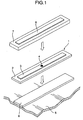
- FIG. 1 shows a structure of a wireless IC tag in accordance with an embodiment 1.
- FIG. 2B is a cross-sectional view of the wireless IC tag of FIG. 1 when taken in its width direction
- FIG. 2A is a cross-sectional view of the wireless IC tag of FIG. 1 when taken in its length direction.
- a base material 2 an antenna (first antenna) 3, and an IC chip 4 form a plate shape, and are collectively called "inlet 1".
- Reference numeral 5 denotes a member on which the wireless IC tag is mounted.
- the wireless IC tag according to embodiment 1 includes the inlet 1 having the first antenna 3 mounted on the base material 2 to be connected to the IC chip 4 having ID information stored therein, a first spacer 6 mounted on a lower surface of the inlet 1 (e.g., on the side of the inlet opposed to the metallic member 5), a second spacer 7 mounted on an upper side of the inlet 1 (on the side of the inlet opposed to the metallic member 5), and a second antenna 8 mounted on the second spacer 7 for acting as a resonator.
- the inlet 1 itself has a structure wherein, for example, the first antenna 3 of a copper foil, which is plated with tin as well as the IC chip 4 having an ID code of 128 bits at the most previously written therein, are arranged on the base material 2 made of polyimide resin.
- the thickness of the first spacer 6 located on the lower surface of the inlet 1 is set at 0.1mm in the example of FIG. 2B , and the material of the first spacer is a foam material having a dielectric constant close to 1. More specifically, the material of the first spacer material is suitably selected from urethane-based, acryl-based or synthetic rubber-based material, considering cost, durability, and adhesivity. No restriction is specifically imposed on the dimensions of the first spacer 6 in its width and length directions.
- the inlet 1 itself is already known. More specifically, for example, 10,000 of the first antennas 3 connected to the respective IC chips 4 are arranged in their width direction in the form of rectangular strips on a plate-shaped base material (meaning a plate material before cut into the base materials 2 having the width dimension, one of which is shown in FIG. 1 ), and then wound into a roll to form a package (which is generally called TCP (tape carrier package) inlet). Or a sheet-like inlet is already known as an inlet material.
- a plate-shaped base material meaning a plate material before cut into the base materials 2 having the width dimension, one of which is shown in FIG. 1
- TCP tape carrier package
- a sheet-like inlet is already known as an inlet material.
- the material of the second spacer 7 mounted on the upper surface of the inlet 1 is an insulating material such as a foam material or a rubber having a dielectric constant close to 1 including a urethane-based, acryl-based or synthetic rubber-based material.
- the thickness of the second spacer 7 is set at 0.3mm. However, no restriction is specifically imposed even on the width or length dimensions of the second spacer 7, and thus such dimensions may be determined from the viewpoint of easy manufacturing.
- the second antenna 8 mounted on the second spacer 7 is formed as a copper foil similarly to the first antenna 3.
- the second antenna 8 is not specifically restricted to the example, but may be formed as an aluminum foil, a conductive ink (a mixture of ink in which carbon resin is incorporated in ink), or the like.
- the thickness of the second antenna is set, for example, at about 0.02mm and the length thereof is set at 53mm from the reason which will be explained later.
- the width dimension of the second antenna 8 is not specifically limited.
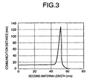
- FIG. 3 is a graph showing a experimental result of a measured communication distance with respect to the length of the second antenna 8 when the insulating material of the second spacer 7 has a constant dielectric constant.
- the communication distance is as constant as about 12mm for the lengths of the second antenna 8 of about 45mm or less.
- the communication distance becomes abruptly long for the lengths of the second antenna exceeding 45mm.
- the second antenna length is 53mm, the communication distance becomes about 130mm.
- the length of the second antenna 8 is further increased, the communication distance becomes abruptly short to the contrary.
- no communication state (communication distance of zero) is established.
- the length of the second antenna 8 is set at 53mm where the communication distance becomes longest.
- the insulating material of the second spacer 7 having a small dielectric constant is advantageous.
- the insulating material of the first spacer 6 and the insulating material of the second spacer 7 may be the same or different from each other.
- the insulating material of the second spacer 7 exerts more influence upon the communication distance than the insulating material of the first spacer 6.
- the first spacer 6 is made of a foam material having a dielectric constant close to air and when the second spacer 7 is made of rubber, the communication distance becomes short because the material of the second spacer 7 has a large dielectric constant.
- the length of the second antenna 8 when the length of the second antenna 8 is set at 1/2 of the wavelength of a radio wave having a predetermined frequency (2.45GHz) to read out information from the wireless IC tag, the communication distance becomes longest.
- the second antenna length varies with the dielectric constant, etc. of the second spacer 7.
- the second spacer 7 is made of an insulating material having a large dielectric constant, the length of the second antenna 8 can be short.
- chloroprene rubber is employed as the insulating material of the second spacer 7, the length of the second antenna 8 can be shortened from 53mm in the above case to 45mm, though its experimental result is not shown.
- the communication distance and the length of the second antenna 8 have a tradeoff relation with respect to the dielectric constant of the employed insulating material of the second spacer 7.
- an insulating material having a suitable dielectric constant is selected; there is realized a wireless IC tag which can make its size small due to addition of the second spacer 7 and the second antenna 8, can shorten its length-directional dimension due to a shortened antenna length, and can secure a relatively long communication distance.
- the length of the first antenna 3 can have the same length as the second antenna 8, that is, be made to be 45mm; the wireless IC tag can be made thin, shorten its length-directional dimension, and be made small in size.
- Table 1 shows an example of the wireless IC tag when the thicknesses of the first and second spacers 6 and 7 are varied.
- the inlet 1 has the same thickness as the second antenna 8.
- Table 1 Example 1
- Example 2 Example 3 Second antenna thickness About 0.02 About 0.02 About 0.02 Second spacer thickness 0.3 0.6 0.6 Inlet (TCP) thickness About 0.1 About 0.1 About 0.1 First spacer thickness 0.1 0.4 1.0 Entire wireless IC tag thickness About 0.5 About 1.1 About 1.7 Unit: mm
- Example 1 when a structure of Example 1 is employed, the wireless IC tag can be made thinnest. For example, when the thickness of the wireless IC tag is preferential, such a wireless IC tag as shown in Example 1 can be used.
- Example 1 is compared with Examples 2 and 3, however, the length of the second antenna 8 is required to have such an accuracy as to be adjusted to a prescribed length depending on a material of the first spacer 6. If the accuracy requirement is not satisfied, then the wireless IC tag varies in communication distance.
- Example 1 corresponds to the wireless IC tag according to the embodiment 1 shown in FIG. 2B .
- the tag is thicker than the wireless IC tag of Example 1.
- the length of the second antenna 8 is not required to have an accuracy as high as Example 1 to be adjusted to the prescribed length.
- the wireless IC tag can secure a communication distance stabler than in the wireless IC tag of Example 1.
- this tag can be used when the thin-dimension requirement of the wireless IC tag is not necessarily preferential and when it is desired to reduce its manufacturing cost by decreasing the number of adjusting steps.
- a wireless IC tag of Example 3 is thicker than the wireless IC tag of Example 2. However, as will be seen from FIG. 6 , the communication distance can be made long by increasing the thickness of the first spacer 6. Thus the tag of Example 3 can be used depending on its application.
- FIG. 4 shows an arrangement of an IC tag system.
- the IC tag system includes a wireless IC tag, an external antenna 30 for transmitting and receiving a radio wave having a predetermined frequency to and from the wireless IC tag, a reader 31 for controlling the transmission and reception of the radio wave at the external antenna 30, and a host computer 32 for instructing the reader 31 to read an ID code stored in the wireless IC tag.
- An RF (radio frequency) transmitter/receiver 311 in the reader 31 outputs/inputs and modulates/demodulates a signal to be transmitted/received; while a controller 312 therein performs communication with the host computer 32 and performs signal transfer to and from the RF transmitter/receiver 311.
- RF radio frequency
- the wireless IC tag produces an operating power larger than the prior art, operates the IC chip 4 with the operating power, reads out the previously-written ID code from the chip, and then transmits the code to the external antenna 30.
- the reader 31 receives the ID code from the wireless IC tag via the external antenna 30; and the controller 312 receives the received ID code from the RF transmitter/receiver 311 and transmits it to the host computer 32.
- the host computer 32 receives and uses the ID code, for example, as information about the member 5 having the wireless IC tag mounted thereon.
- the communication distance of the prior art wireless IC tag is merely 10mm, whereas the communication distance of the wireless IC tag of the embodiment 1 can be made to be 130mm as mentioned above.
- a distance between the wireless IC tag and the external antenna 30 in FIG. 4 can be made to be 130mm.
- an exclusive external antenna enabling a short communication distance
- the present invention can use a general external antenna commonly used because the communication distance can be made long as mentioned above.
- the member 5, on which the wireless IC tag of the embodiment 1 can be suitably mounted may be made of not only the metallic material as mentioned above but also a glass member containing water or a material such as animal body containing much water and having a large dielectric constant, as an example.
- the communication distance for the predetermined frequency was able to be made about 13 times longer than the communication distance of the prior art wireless IC tag, while suppressing the entire thickness of the wireless IC tag.
- the first and second spacers 6 and 7 are made of an insulating material and the thickness of the second spacer 7 is made larger than that of the first spacer 6, a more effective wireless IC tag can be realized by increasing the communication distance.
- an adhesive can be employed for the purpose of joining the antennas and the spacers in the wireless IC tag.
- FIG. 5 schematically shows a structure of an apparatus for manufacturing such a wireless IC tag (as having the structure shown in FIG. 1 ). Constituent elements having the same functions or structures as in FIG. 1 are denoted by the same reference numerals.
- diagrams shown as surrounded by respective circles in the vicinity of an inlet material 11, a first spacer material 12, a second spacer material 13 and a second antenna material 14, to be explained later, are views when parts of the respective materials are viewed from their planes.
- a diagram shown as surrounded by a circle in the lower right side of FIG. 5 is a perspective view of the wireless IC tag (having a structure similar to that of FIG. 1 ) manufactured by the wireless IC tag manufacturing apparatus.
- reference numeral 11 denotes the first antenna material (more specifically, the inlet material).
- the first antenna material more specifically, the inlet material.
- the first spacer material as a foam material (meaning a plate material before cut into strips of the width dimension of the first spacer 6 in FIG. 1 ).
- a double-coated tape is applied onto one surface of the first spacer material 12 as an adhesive surface, under which condition the first spacer material is wound into a roll.
- Numeral 13 denotes the second spacer material as a foam material (meaning a plate material before cut into strips of the width dimension of the second spacer 7 in FIG. 1 ).
- a double-coated tape is applied to both sides of the second spacer material, under which condition the second spacer material is wound into a roll.
- Numeral 14 denotes the second antenna material on which, for example, 10,000 of the second antennas 8 are arranged in their width direction in the form of strips with a protective film as a base material, under which condition the second antenna material is wound into a roll.
- the shape of the second antenna material 14 is not limited to the strip but a plate material such as a copper plate may be sometimes used. In the latter case, as will be explained later, the plate material is cut into pieces of a width dimension similar to the first or second spacer 6 or 7, and eventually manufactured as wireless IC tags.
- Numeral 15 denotes a roller provided with a sprocket which engages with, e.g., holes (not shown) made in both ends of the inlet material 11 being fed out by a not-shown drive source to be spaced at equal intervals.
- Numeral 16 denotes a first feeding roller which compresses the coming first antenna material 11 and the first spacer material 12 being fed by a not-shown drive source, and feeds out the compressed material forward (in an arrow direction).
- Numeral 17 denotes a second feeding member which further compresses the plate materials being compressed and fed by the first feeding roller 16 together with the second spacer material 13 being fed by a not-shown drive source, and feeds out the compressed materials forward (in an arrow direction).
- Numeral 18 denotes a third feeding member which further compresses the plate materials being compressed and fed out by the second feeding member 17 together with the second antenna material 14 being fed out by a not-shown drive source, and feeds out the compressed materials forward (in an arrow direction).
- Numeral 19 denotes a position detector which generates a signal to control the timing of feeding out the second antenna material 14. The position detector 19 becomes necessary when the second antennas 8 are parallelly arranged in their width direction in the form of strips as shown in FIG. 5 .
- Numeral 20 denotes a position detector which generates a signal to control the timing of cutting the wireless IC tag material being fed out by the third feeding member 18 with use of a cutter 21.
- Numeral 22 denotes a fixing base which is used as a base when the wireless IC tag material is cut by the cutter 21 and also as a base on which one wireless IC tag shown in FIG. 1 is mounted.
- the first spacer material 12 is guided by a not-shown drive source, e.g., along a guide rail for restricting its width-directional position, and then fed out to the first feeding roller 16.
- the first antenna material 11 is guided by the not-shown drive source, e.g., along a guide rail for restricting its width-direction position, and then fed out until the not-shown holes made in the both ends of the inlet material engages with the sprocket of the roller 15. The engaged inlet material is then fed out toward the first feeding roller 16.
- the second spacer material 13 is also guided by the not-shown drive source along a guide rail for restricting its width-directional position and fed out toward the second feeding member 17.
- a cover covering one surface of the second spacer material 13 is peeled off as shown by a dashed line (simultaneously is subjected to antistatic treatment), and fed out toward the second feeding member 17.
- the plate material being fed out by the first feeding roller 16 reaches the position of the second feeding member 17, the plate material is bonded to one surface of the second spacer material 13 and compressed together, and then fed out toward the third feeding member 18.
- the other surface of the second spacer material 13 is also an adhesive surface.
- the second antenna material 14 is also guided by the not-shown drive source, e.g., along a rail guide for restricting its width-directional position, and then fed out toward the third feeding member 18.
- the plate material having the three-layer structure being fed out from the second feeding member 17 reaches the position of the third feeding member 18, the plate material is bonded to the other adhesive surface of the second spacer material 13, compressed together, and then fed out toward the cutter 21 as a wireless IC tag material having a four-layer structure.
- the second antenna material 14 is made up of a predetermined number of such second antennas 8 as shown in FIG. 5 arranged parallelly in their width direction in the form of strips, it becomes necessary to control the timing of feeding out the second antenna material 14 in such a manner that, upon the compression of the third feeding member 18, the position of one of the second antennas 8 coincides with the position of one of the first antennas 3 of the first antenna material 11.
- the position detector 19 generates its timing signal. That is, on the basis of a signal from the position detector 19, the driving of the not-shown drive source for feeding out the second antenna material 14 is controlled.
- the second antenna material 14 is a plate-shaped material like the first or second spacer material 12 or 13, however, the second antenna material is required to be cut into strips having the same width when the first spacer 6 and the second spacer 7 are cut. For this reason, the control of the feeding-out timing by the position detector 19 becomes unnecessary, which will be explained later.
- the position detector 20 When the wireless IC tag material of the four-layer structure is fed out from the third feeding member 18 and reaches the position of the cutter 21, the tag material is sequentially cut into strips having such a width dimension as shown in FIG. 1 . In this manner, a wireless IC tag having a structure similar to in FIG. 1 is manufactured.
- the position detector 20 For the above cutting timing, the position detector 20 generates a timing signal as mentioned above. In other words, the cutter 21 is operated on the basis of a signal from the position detector 20.
- the cutting timing is set at a time point when the position detector 20 detects a marking position indicative of the cutting position previously marked at a width-directional end of the first antenna material 11 (more specifically, the plate-shaped base material 2A).
- the cutting timing is not limited to the above example.
- the width dimension of the second antenna 8 is not the same as the width of the second antenna 8 shown in FIG. 1 , and the second antenna material is cut into strips having a width dimension similar to the first or second spacer 6 or 7.
- the material having the four-layer structure is cut off into individual wireless IC tag strips, after-treatment of such tags becomes troublesome (the wireless IC tags are randomly oriented on the fixing base 22). For this reason, it is desirable to cut the second antenna material 14, the second spacer material 13, and the first antenna material 11 in the tag material; but to perforate the first spacer material 12 as the lowermost layer. As a result, the manufactured wireless IC tags can be also partly uncut and thus be arranged on the fixing base 22.
- the adhesive surfaces are exposed to the cut surfaces thereof.
- it is necessary to remove the adhesion of the adhesive surface for example, by sprinkling power thereover and by removing unnecessary remained powder or by other suitable means.
- a wireless IC tag using a first antenna, a first spacer, a second antenna, and a second spacer can be manufactured.
- a plate-shaped first antenna, a plate-shaped first spacer, a plate-shaped second antenna, and a plate-shaped second spacer can be used.
- the followings may be used: a first antenna material, a plate-shaped first spacer material, a plate-shaped second spacer material, a plate-shaped second spacer material, and a plate-shaped second antenna material wherein a predetermined number of second antennas are arranged in their width direction in the form of strips.
- an apparatus for manufacturing a wireless IC tag can be realized with use of the plate-shaped first antenna material, the plate-shaped first spacer material, the plate-shaped second antenna material, and the plate-shaped second spacer material.
- the followings may be used to realize an apparatus for manufacturing a wireless IC tag: a plate-shaped first antenna material, a plate-shaped first spacer material, a predetermined member of plate-shaped second spacer material, a second antenna material wherein a predetermined number of plate-shaped second antennas are arranged in their width direction in the form of strips.
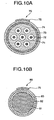
- FIGS. 10A and 10B show a conceptual view of a condition when a wireless IC tag is mounted onto a cable in the prior art, wherein FIG. 10A is a condition when the tag is mounted to a multicore cable, and FIG. 10B is a condition when the tag is mounted onto a single core cable. As shown in FIG. 10A is a condition when the tag is mounted to a multicore cable, and FIG. 10B is a condition when the tag is mounted onto a single core cable. As shown in FIG.
- a multicore cable 70 used as a communication cable a plurality of internal conductors 72 as multiple cores each coated with single core envelope 71 are surrounded by a shield layer 73, which in turn is further covered with a cable enclosure 74. And a wireless IC tag 75 is bonded onto the surface of the cable enclosure 74 with an adhesive or the like.
- an internal conductor 81 is covered with a single core envelope 82, which in turn is coated with a cable enclosure 83.
- a wireless IC tag 75 is bonded onto the surface of the cable enclosure 83 with an adhesive or the like.
- the wireless IC tag 75 is generally made of an antenna and an IC chip mounted on a rectangular substrate having a desired small dielectric constant.
- a plurality of such wireless IC tags 75 are bonded onto the multicore cable 70 or the single core cable 80 along its length direction at intervals of, e.g., 1m.
- wireless IC tags 75 tend to be easily peeled off from the cable enclosure 74 (or the cable enclosure 83) because the tags are merely bonded thereon with the adhesive or the like. Further, the communication distance is prevented from being reduced by increasing a spacing between the wireless IC tag 75 and a metallic part (i.e., the shield layer 73 in FIG. 10A or the internal conductor 81 in FIG. 10B ) within the cable depending on the thickness of the cable enclosure 74 (or the cable enclosure 83). However, the thickness of the cable enclosure 74 (or the cable enclosure 83) is determined by cable specifications. Thus when the thickness is not sufficient, the communication distance between the wireless IC tag 75 and a reader (not shown) become short.
- the cable enclosure 74 (or the cable enclosure 83) is also heated to a high temperature.
- the wireless IC tag 75 is mounted in the interior of the cable enclosure 74 during its manufacturing steps, the tag is thermally destroyed, disabling mounting of the tag in the cable enclosure. For this reason, a step of bonding the wireless IC tag 75 after completion of the manufacturing steps is required to be added, which leads to the fact that the cable manufacturing cost becomes high.
- a glass epoxy substrate or the like having a high heat resistance is used as a tag base material (i.e., a second spacer), an antenna electrode is deposited on the front or back surfaces of the substrate to form a wireless IC tag.
- the wireless IC tag is buried in the interior of the cable enclosure. As a result, it can be avoided that high temperature during the cable molding cause deterioration of the tag base material and malfunction of the tag. During handling of the cable, further, the wireless IC tag can be prevented from being peeled off from the cable.
- the antenna electrodes formed on the front and back surface of the tag base material are used as first and second antennas, it can be avoided that the communication distance of the wireless IC tag be undesirably reduced under the influence of the metallic part (i.e., shield layer or internal conductor) of the cable, as mentioned in connection with the embodiment 1.
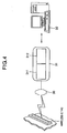
- FIGS. 7A and 7B show a conceptual view of a wireless IC tag employed in an embodiment 5, wherein FIG. 7A is a perspective view of the tag and FIG. 7B is a cross-sectional view when taken line A-A in FIG. 7A .
- a thin film metallic antenna is deposited on a surface of a heat-resistance second spacer 7a of a glass epoxy material having a desired dielectric constant to form a first antenna 3a.
- a thin film metallic antenna is deposited on the rear surface of the second spacer 7a at a location opposed to the first antenna 3a to form a second antenna 8a.
- An IC chip 4 is mounted on the first antenna 3a nearly in the center thereof.
- the second antenna 8a functions as an auxiliary antenna for resonating to a desired frequency of a radio wave radiated from the first antenna 3a to strengthen the intensity of the radio wave. Accordingly, even when a metallic member is provided in the vicinity of the first antenna 3a, the intensity of the radio wave of the first antenna 3a can be prevented from being made weak thereby, which has already been explained in detail in the foregoing embodiment 1 and thus explanation thereof is omitted herein.
- the size, thickness, etc. of the second spacer 7a, the first antenna 3a, and the second antenna 8a have been explained in the foregoing embodiment 1, and therefore explanation thereof is omitted. Since the wireless IC tag 25 thus formed has a small elongated shape, the tag can be easily buried within the cable enclosure along the length direction of the cable during the cable molding operation. Due to the action of the auxiliary antenna of the second antenna 8a, a radio wave can be transmitted from the first antenna 3a without being weakened by the internal conductor (i.e., metal) of the cable. Since the second spacer 7a is made of a glass epoxy material, the spacer can sufficiently withstand a temperature as high as about 200-300°C during the cable molding. In this connection, the IC chip 4 has a thermal breakdown temperature not lower than 300°C.
- FIGS. 8A and 8B show a conceptual view of a condition when a wireless IC tag is mounted to a cable, wherein FIG. 8A is a condition when the tag is mounted in a multicore cable and FIG. 8B is a condition when the tag is mounted in a power cable.
- FIG. 8A in a multicore cable 40 used as a communication cable, a plurality of internal conductors 42 each covered with a single core envelope 41 are surrounded by a shield layer 43, which in turn is covered with a cable enclosure 44.
- the wireless IC tag 25 mounted during its molding is buried in the interior of the cable enclosure 44.
- an internal conductor 51 is covered with a single core envelope 52, which in turn is covered with a cable enclosure 53.
- the wireless IC tag 25 mounted during the molding is buried in the interior of the cable enclosure 53.
- Such wireless IC tags 25 are buried along the length direction of the multicore cable 40 or the single core cable 50 at intervals of, e.g., 1m.
- the wireless IC tag 25 can be mounted in the cable enclosure 44 or the cable enclosure 53 without being thermally destroyed, and it can be avoided that the wireless IC tag 25 be peeled off from the multicore cable 40 or the single core cable 50 during cable handling.
- the wireless IC tag 25 since the first antenna 3a and the second antenna 8a as the auxiliary antenna are formed on the front and back surface of the second spacer as shown in FIGS. 7A and 7B , it can be avoided that radio wave be adversely influenced by the shield layer 43 in the multicore cable 40 or by the metallic layer of the internal conductor 51 in the single core cable 50. Accordingly, the wireless IC tag 25 can secure a sufficient communication distance.
- the provision of the first and second antennas 3a and 8a enables prevention of reduction of the communication distance caused by the metallic layer, which has already been explained in the embodiment 1 and explanation thereof is omitted.
- the cable enclosure 44 (or the cable enclosure 53) is used as a first spacer. Therefore, the cable enclosure 44 (or the cable enclosure 53) is required to be controlled to have a desired thickness.
- FIGS. 9A to 9D show steps of manufacturing a wireless IC tag to be buried in a cable enclosure in the present embodiment.
- a first step of FIG. 9A aluminum, copper or similar substance are deposited at an equal pitch intervals on the surface of a glass epoxy substrate 61 to form a multiplicity of first antennas 3a as thin films.
- aluminum, copper or similar substance is deposited on the rear surface of the glass epoxy substrate 61 at positions opposed to the first antennas 3a to form a multiplicity of second antennas 8a.
- the first antennas 3a and the second antennas 8a may be formed as thin films on the front and back surface of the glass epoxy substrate 61 by an etching process.
- a second step of FIG. 9B next, an IC chip 4 is mounted nearly in the center of each of the multiplicity of first antennas 3a, and terminals of the IC chips 4 are connected to the respective first antennas 3a.
- the substrate is cut along cutout lines previously made in the glass epoxy substrate 61 into a multiplicity of individual wireless IC tags.
- a wireless IC tag 25 that the first antenna 3a and the IC chip 4 are positioned on one surface of the second spacer 7a of a glass epoxy substrate and the second antenna 8a, is positioned on the other surface thereof as shown in FIGS. 7A and 7B can be manufactured.
- a single wireless IC tag 25 is buried in the interior of a cable enclosure 66 at a predetermined position during cable molding in steps of manufacturing a cable 65 (single core cable).
- such wireless IC tags 25 are buried in the cable enclosure 66, for example, along the length direction of the cable 65 at interval of 1m and simultaneously molded.
- the thickness of the cable enclosure 66 is not sufficient, as shown in FIG. 9D , a part of the cable enclosure where the wireless IC tag 25 is to be mounted is raised, the tag 25 is buried in the raised part to be spaced by a predetermined distance from the internal conductor 51.
- the wireless IC tag 25 can be prevented from coming off from the cable 65, can secure a desired communication distance, and can be prevented from being thermally destroyed during the cable molding. That is, since the wireless IC tag can withstand such a high temperature during the cable molding, the tag can be mounted in the cable enclosure. Whereby the wireless IC tag can be avoided from coming off from the cable, and its communication distance can be made long.
- the present invention is not limited to the above examples but the invention can be implemented in the form of another embodiment.
- the wireless IC tag is considered to have a multi-layered structure of spacers and antennas, as by further laminating a third spacer and a third antenna on the second antenna and laminating a fourth spacer and a fourth antenna on the third antenna, and so on.
- the frequency of radio wave is also not limited to 2.45GHz mentioned above but the invention can be realized in another frequency.
- the present invention can be realized, for example, even when a heat resistance substrate made of ceramic or fluorine resin (e.g., Teflon (registered trademark)) is used as the second spacer.
- a heat resistance substrate made of ceramic or fluorine resin e.g., Teflon (registered trademark)
Landscapes
- Physics & Mathematics (AREA)
- Engineering & Computer Science (AREA)
- General Physics & Mathematics (AREA)
- Electromagnetism (AREA)
- Theoretical Computer Science (AREA)
- Microelectronics & Electronic Packaging (AREA)
- Computer Hardware Design (AREA)
- Automation & Control Theory (AREA)
- Computer Security & Cryptography (AREA)
- Health & Medical Sciences (AREA)
- Toxicology (AREA)
- Computer Networks & Wireless Communication (AREA)
- General Health & Medical Sciences (AREA)
- Artificial Intelligence (AREA)
- Computer Vision & Pattern Recognition (AREA)
- Details Of Aerials (AREA)
- Burglar Alarm Systems (AREA)
- Insulated Conductors (AREA)
- Aerials With Secondary Devices (AREA)
Description
- The present invention relates to wireless IC tags suitable for mounting on a member having a large dielectric constant, and methods and apparatuses for manufacturing the wireless IC tags; and in particular, to a wireless IC tag suitable for mounting on a power cable, a communication cable or the like, and a method and apparatus for manufacturing the wireless IC tags.
- For the purpose of article management, theft or fake prevention; a wireless tag for obtaining information on an article in a non-contact manner has been developed and put to practical use. For example,
JP-A-11-339142 JP-A-11-339142 - Also disclosed in
JP-A-2003-203527 -
WO 031 07 292 - The aforementioned wireless tag, however, has a problem that, when the wireless tag is bonded to a metallic article, a radio wave received by the wireless tag is absorbed in the metallic article, which results in that the intensity of radio wave to be transmitted from the wireless tag becomes weak and thus its detectable distance becomes short.
- This problem similarly arises even in the wireless IC tag having an IC chip added to the wireless tag. The wireless IC tag is made up of a base material, an antenna as a metallic foil formed on the base material, an IC chip provided on the antenna and having information previously written therein, and a spacer disposed between the base material and the article. A radio wave having a predetermined frequency is transmitted from an external antenna to the wireless IC tag; the tag produces an operating power from the radio wave received from the antenna to operate the IC chip, reads out the information previously written in the IC chip, and transmits the information from the antenna. The information is received by the external antenna. When the wireless IC tag is used to be bonded to the metallic article or the like, the radio wave received by the wireless IC tag is absorbed in the metallic article. Thus, the tag cannot obtain a sufficient operating power, eventually leading to the fact that the tag cannot operate the IC chip to read the information, nor transmit the information as far as a position away by a necessary distance.
- In order to solve the problem, the spacer is required to be made thick. Since the thick spacer leads to an increase in the size of the wireless IC tag (an increase in the thickness in this example), this method cannot be easily employed.
-
FIG. 6 is a graph showing a communication distance characteristic when the thickness of the spacer in the aforementioned prior art wireless IC tag is varied. When the spacer thickness is 1mm, a communication distance is as short as about 10mm. On the contrary, in order to make the communication distance longest (about 150mm), a spacer is required to have a thickness not smaller than 15mm. In this case, however, the antenna is assumed to have a length of 53mm. - When the spacer thickness is increased in this manner, the communication distance can be made longer. However, when the spacer thickness is increased to obtain a long communication distance, this involves a large-sized wireless IC tag. As a result, its application field is limited as a big hindrance. Even when such a large tag is actually used, the tag may be possibly peeled off by the person's or object's contact with the tag, with a bad handleability.
- Even when such a tag is mounted to a cable, the communication distance of the tag is remarkably reduced, because the interior of the cable may be a metallic conductor such as copper or a metallic shield layer may be applied to the inside of an outer layer thereof. Further, when the wireless IC tag is bonded and mounted onto the surface of the cable, the tag may be easily dismounted. In addition, when the wireless IC tag is buried in the interior of the cable, the substrate of the tag cannot withstand a high temperature when the cable is molded. In this way, the problem with the bad handleability when the wireless IC tag is used for the cable, is not solved still.
- The present invention has been made in view of such a problem, and it is an object of the invention to provide a wireless IC tag which can have a small thickness and a long communication distance even when mounted in the vicinity of a metallic part and which can have less likelihood of being dismounted or destroyed by a high temperature even when mounted to a cable or the like, and also to provide a method and apparatus for manufacturing the wireless IC tag.
- In order to solve the aforementioned problem, a wireless IC tag in accordance with the present invention includes a first antenna and a first spacer. The tag produces an operating power from a radio wave having a predetermined frequency and received at the first antenna to operate an IC chip, reads out and transmit identification information stored in the chip. The tag also includes a second antenna having a predetermined length and having an auxiliary function of resonating to a radio wave having a predetermined frequency and strengthening an radio wave to be transmitted from the first antenna, and a second spacer disposed between the first and second antennas for holding a distance between the both antennas.
- In the present invention, further, a heat resistance substrate made of glass epoxy, ceramic or fluorine resin is used as the second spacer to withstand a high temperature when a cable is molded. In order to secure a desired communication distance even when a metallic conductor or a shield layer is present in the interior of the cable, the first and second antennas are made in the form of thin films by metallic deposition on both sides of the second spacer, and an auxiliary function of strengthening the radio wave to be transmitted from the first antenna is provided to the second antenna.
- Other objects, features and advantages of the invention will become apparent from the following description of the embodiments of the invention taken in conjunction with the accompanying drawings.
-
-
FIG. 1 is a perspective view showing a structure of a wireless IC tag in accordance with anembodiment 1; -
FIG. 2A is a cross-sectional view of the wireless IC tag of theembodiment 1 when taken in its width direction; -
FIG. 2B is a cross-sectional view of the wireless IC tag of theembodiment 1 when taken in its length direction; -
FIG. 3 is a graph showing a communication distance characteristic with respect to the length of a second antenna of the wireless IC tag of theembodiment 1; -
FIG. 4 is an arrangement of an IC tag system including the wireless IC tag of theembodiment 1, a reader for transmitting a radio wave having a predetermined frequency to the wireless IC tag, an external antenna, and a host computer; -
FIG. 5 is a structure of an apparatus for manufacturing a wireless IC tag in accordance with anembodiment 2; -
FIG. 6 is a graph showing a communication distance characteristic with respect to the thickness of a first spacer in a prior art wireless IC tag; -
FIG. 7A is a perspective view showing a structure of a wireless IC tag when applied as anembodiment 3; -
FIG. 7B shows a cross-sectional view ofFIG. 7A when taken along line A-A; -
FIG. 8A shows a state of a mounting step when the wireless IC tag is mounted in a multicore cable; -
FIG. 8B shows a state of a mounting step when the wireless IC tag is mounted in a single core cable; -
FIG. 9A shows one of steps of manufacturing the wireless IC tag to be buried in an outer layer or enclosure of a cable in the present invention; -
FIG. 9B shows one of steps of manufacturing the wireless IC tag to be buried in the enclosure of the cable in the present invention; -
FIG. 9C shows one of steps of manufacturing the wireless IC tag to be buried in the enclosure of the cable in the present invention; -
FIG. 9D shows one of steps of manufacturing the wireless IC tag to be buried in the enclosure of the cable in the present invention; -
FIG. 10A shows a state of a mounting step when a wireless IC tag is mounted onto a multicore cable in a prior art; and -
Fig. 10B shows a state of a mounting step when the wireless IC tag is mounted onto a single core cable in the prior art. - Embodiments of the present invention will be explained in detail with reference to accompanying drawings.
-
FIG. 1 shows a structure of a wireless IC tag in accordance with anembodiment 1.FIG. 2B is a cross-sectional view of the wireless IC tag ofFIG. 1 when taken in its width direction, andFIG. 2A is a cross-sectional view of the wireless IC tag ofFIG. 1 when taken in its length direction. Among members of the wireless IC tag shown inFIG. 1 ; abase material 2, an antenna (first antenna) 3, and anIC chip 4 form a plate shape, and are collectively called "inlet 1".Reference numeral 5 denotes a member on which the wireless IC tag is mounted. The wireless IC tag according toembodiment 1 includes theinlet 1 having thefirst antenna 3 mounted on thebase material 2 to be connected to theIC chip 4 having ID information stored therein, afirst spacer 6 mounted on a lower surface of the inlet 1 (e.g., on the side of the inlet opposed to the metallic member 5), asecond spacer 7 mounted on an upper side of the inlet 1 (on the side of the inlet opposed to the metallic member 5), and asecond antenna 8 mounted on thesecond spacer 7 for acting as a resonator. - The
inlet 1 itself has a structure wherein, for example, thefirst antenna 3 of a copper foil, which is plated with tin as well as theIC chip 4 having an ID code of 128 bits at the most previously written therein, are arranged on thebase material 2 made of polyimide resin. The thickness of thefirst spacer 6 located on the lower surface of theinlet 1 is set at 0.1mm in the example ofFIG. 2B , and the material of the first spacer is a foam material having a dielectric constant close to 1. More specifically, the material of the first spacer material is suitably selected from urethane-based, acryl-based or synthetic rubber-based material, considering cost, durability, and adhesivity. No restriction is specifically imposed on the dimensions of thefirst spacer 6 in its width and length directions. - The
inlet 1 itself is already known. More specifically, for example, 10,000 of thefirst antennas 3 connected to therespective IC chips 4 are arranged in their width direction in the form of rectangular strips on a plate-shaped base material (meaning a plate material before cut into thebase materials 2 having the width dimension, one of which is shown inFIG. 1 ), and then wound into a roll to form a package (which is generally called TCP (tape carrier package) inlet). Or a sheet-like inlet is already known as an inlet material. - The material of the
second spacer 7 mounted on the upper surface of theinlet 1 is an insulating material such as a foam material or a rubber having a dielectric constant close to 1 including a urethane-based, acryl-based or synthetic rubber-based material. In the example ofFIG. 2B , the thickness of thesecond spacer 7 is set at 0.3mm. However, no restriction is specifically imposed even on the width or length dimensions of thesecond spacer 7, and thus such dimensions may be determined from the viewpoint of easy manufacturing. - The
second antenna 8 mounted on thesecond spacer 7 is formed as a copper foil similarly to thefirst antenna 3. However, thesecond antenna 8 is not specifically restricted to the example, but may be formed as an aluminum foil, a conductive ink (a mixture of ink in which carbon resin is incorporated in ink), or the like. The thickness of the second antenna is set, for example, at about 0.02mm and the length thereof is set at 53mm from the reason which will be explained later. The width dimension of thesecond antenna 8 is not specifically limited. -
FIG. 3 is a graph showing a experimental result of a measured communication distance with respect to the length of thesecond antenna 8 when the insulating material of thesecond spacer 7 has a constant dielectric constant. As shown inFIG. 3 , the communication distance is as constant as about 12mm for the lengths of thesecond antenna 8 of about 45mm or less. However, as the length of thesecond antenna 8 is increased, the communication distance becomes abruptly long for the lengths of the second antenna exceeding 45mm. When the second antenna length is 53mm, the communication distance becomes about 130mm. As the length of thesecond antenna 8 is further increased, the communication distance becomes abruptly short to the contrary. And when the length of the second antenna reaches about 60mm, no communication state (communication distance of zero) is established. In theembodiment 1, on the basis of this experimental result, the length of thesecond antenna 8 is set at 53mm where the communication distance becomes longest. - In order to make the communication distance long, the insulating material of the
second spacer 7 having a small dielectric constant is advantageous. Further, the insulating material of thefirst spacer 6 and the insulating material of thesecond spacer 7 may be the same or different from each other. However, it is known that the insulating material of thesecond spacer 7 exerts more influence upon the communication distance than the insulating material of thefirst spacer 6. For example, when thefirst spacer 6 is made of a foam material having a dielectric constant close to air and when thesecond spacer 7 is made of rubber, the communication distance becomes short because the material of thesecond spacer 7 has a large dielectric constant. - It is theoretically known that, when the length of the
second antenna 8 is set at 1/2 of the wavelength of a radio wave having a predetermined frequency (2.45GHz) to read out information from the wireless IC tag, the communication distance becomes longest. However, the second antenna length varies with the dielectric constant, etc. of thesecond spacer 7. When thesecond spacer 7 is made of an insulating material having a large dielectric constant, the length of thesecond antenna 8 can be short. For example, it is known that, when chloroprene rubber is employed as the insulating material of thesecond spacer 7, the length of thesecond antenna 8 can be shortened from 53mm in the above case to 45mm, though its experimental result is not shown. - In this way, the communication distance and the length of the
second antenna 8 have a tradeoff relation with respect to the dielectric constant of the employed insulating material of thesecond spacer 7. For this reason, when an insulating material having a suitable dielectric constant is selected; there is realized a wireless IC tag which can make its size small due to addition of thesecond spacer 7 and thesecond antenna 8, can shorten its length-directional dimension due to a shortened antenna length, and can secure a relatively long communication distance. In the aforementioned example, since the length of thefirst antenna 3 can have the same length as thesecond antenna 8, that is, be made to be 45mm; the wireless IC tag can be made thin, shorten its length-directional dimension, and be made small in size. - Table 1 shows an example of the wireless IC tag when the thicknesses of the first and
second spacers inlet 1 has the same thickness as thesecond antenna 8.Table 1 Example 1 Example 2 Example 3 Second antenna thickness About 0.02 About 0.02 About 0.02 Second spacer thickness 0.3 0.6 0.6 Inlet (TCP) thickness About 0.1 About 0.1 About 0.1 First spacer thickness 0.1 0.4 1.0 Entire wireless IC tag thickness About 0.5 About 1.1 About 1.7 Unit: mm - As shown in Table 1, when a structure of Example 1 is employed, the wireless IC tag can be made thinnest. For example, when the thickness of the wireless IC tag is preferential, such a wireless IC tag as shown in Example 1 can be used. When Example 1 is compared with Examples 2 and 3, however, the length of the
second antenna 8 is required to have such an accuracy as to be adjusted to a prescribed length depending on a material of thefirst spacer 6. If the accuracy requirement is not satisfied, then the wireless IC tag varies in communication distance. Example 1 corresponds to the wireless IC tag according to theembodiment 1 shown inFIG. 2B . - In the case of a wireless IC tag of Example 2, the tag is thicker than the wireless IC tag of Example 1. However, the length of the
second antenna 8 is not required to have an accuracy as high as Example 1 to be adjusted to the prescribed length. And even when the accuracy requirement is not satisfied, the wireless IC tag can secure a communication distance stabler than in the wireless IC tag of Example 1. For example, this tag can be used when the thin-dimension requirement of the wireless IC tag is not necessarily preferential and when it is desired to reduce its manufacturing cost by decreasing the number of adjusting steps. - As shown even in Examples 1, 2 and 3, for the purpose of increasing the communication distance, it is desirable to make the
second spacer 7 thicker than thefirst spacer 6. - A wireless IC tag of Example 3 is thicker than the wireless IC tag of Example 2. However, as will be seen from
FIG. 6 , the communication distance can be made long by increasing the thickness of thefirst spacer 6. Thus the tag of Example 3 can be used depending on its application. - Explanation will next be made as to the operation of a system using the wireless IC tag (sometimes by referring to
FIG. 1 ). -
FIG. 4 shows an arrangement of an IC tag system. The IC tag system includes a wireless IC tag, anexternal antenna 30 for transmitting and receiving a radio wave having a predetermined frequency to and from the wireless IC tag, areader 31 for controlling the transmission and reception of the radio wave at theexternal antenna 30, and ahost computer 32 for instructing thereader 31 to read an ID code stored in the wireless IC tag. An RF (radio frequency) transmitter/receiver 311 in thereader 31 outputs/inputs and modulates/demodulates a signal to be transmitted/received; while acontroller 312 therein performs communication with thehost computer 32 and performs signal transfer to and from the RF transmitter/receiver 311. - Explanation will be made in connection with an example when the ID code stored in the wireless IC tag mounted on the
metallic member 5 is read out. When thecontroller 312 in thereader 31 receives an instruction from thehost computer 32 to read the ID code stored in the wireless IC tag, the controller controls the RF transmitter/receiver 311 to transmit a radio wave having a predetermined frequency (2.45GHz) from theexternal antenna 30 to the wireless IC tag. Thesecond antenna 8 on the side of the wireless IC tag when receiving the radio wave resonates to thefirst antenna 3 when receiving the wave similarly. As a result, the wireless IC tag produces an operating power larger than the prior art, operates theIC chip 4 with the operating power, reads out the previously-written ID code from the chip, and then transmits the code to theexternal antenna 30. Thereader 31 receives the ID code from the wireless IC tag via theexternal antenna 30; and thecontroller 312 receives the received ID code from the RF transmitter/receiver 311 and transmits it to thehost computer 32. Thehost computer 32 receives and uses the ID code, for example, as information about themember 5 having the wireless IC tag mounted thereon. - The communication distance of the prior art wireless IC tag is merely 10mm, whereas the communication distance of the wireless IC tag of the
embodiment 1 can be made to be 130mm as mentioned above. Thus, a distance between the wireless IC tag and theexternal antenna 30 inFIG. 4 can be made to be 130mm. As a result, although an exclusive external antenna (enabling a short communication distance) suitable for such a member having a large dielectric constant as themetallic member 5 has been required to be used as theexternal antenna 30 in the prior art, the present invention can use a general external antenna commonly used because the communication distance can be made long as mentioned above. - In this connection, the
member 5, on which the wireless IC tag of theembodiment 1 can be suitably mounted, may be made of not only the metallic material as mentioned above but also a glass member containing water or a material such as animal body containing much water and having a large dielectric constant, as an example. - In the
embodiment 1, the communication distance for the predetermined frequency was able to be made about 13 times longer than the communication distance of the prior art wireless IC tag, while suppressing the entire thickness of the wireless IC tag. When the first andsecond spacers second spacer 7 is made larger than that of thefirst spacer 6, a more effective wireless IC tag can be realized by increasing the communication distance. In this connection, for the purpose of joining the antennas and the spacers in the wireless IC tag, an adhesive can be employed. -
FIG. 5 schematically shows a structure of an apparatus for manufacturing such a wireless IC tag (as having the structure shown inFIG. 1 ). Constituent elements having the same functions or structures as inFIG. 1 are denoted by the same reference numerals. InFIG. 5 , diagrams shown as surrounded by respective circles in the vicinity of aninlet material 11, afirst spacer material 12, asecond spacer material 13 and asecond antenna material 14, to be explained later, are views when parts of the respective materials are viewed from their planes. A diagram shown as surrounded by a circle in the lower right side ofFIG. 5 is a perspective view of the wireless IC tag (having a structure similar to that ofFIG. 1 ) manufactured by the wireless IC tag manufacturing apparatus. - In
FIG. 5 ,reference numeral 11 denotes the first antenna material (more specifically, the inlet material). As already explained earlier, it is already known that, for example, 10,000 of thefirst antennas 3 connected with the IC chips 4 inFIG. 1 are arranged in their width direction in the form of rectangular strips on a plate-shapedbase material 2A, and then wound to form a TCP inlet. Such an inlet can be used as it is.Numeral 12 denotes the first spacer material as a foam material (meaning a plate material before cut into strips of the width dimension of thefirst spacer 6 inFIG. 1 ). For example, a double-coated tape is applied onto one surface of thefirst spacer material 12 as an adhesive surface, under which condition the first spacer material is wound into a roll.Numeral 13 denotes the second spacer material as a foam material (meaning a plate material before cut into strips of the width dimension of thesecond spacer 7 inFIG. 1 ). For example, a double-coated tape is applied to both sides of the second spacer material, under which condition the second spacer material is wound into a roll.Numeral 14 denotes the second antenna material on which, for example, 10,000 of thesecond antennas 8 are arranged in their width direction in the form of strips with a protective film as a base material, under which condition the second antenna material is wound into a roll. The shape of thesecond antenna material 14 is not limited to the strip but a plate material such as a copper plate may be sometimes used. In the latter case, as will be explained later, the plate material is cut into pieces of a width dimension similar to the first orsecond spacer -
Numeral 15 denotes a roller provided with a sprocket which engages with, e.g., holes (not shown) made in both ends of theinlet material 11 being fed out by a not-shown drive source to be spaced at equal intervals.Numeral 16 denotes a first feeding roller which compresses the comingfirst antenna material 11 and thefirst spacer material 12 being fed by a not-shown drive source, and feeds out the compressed material forward (in an arrow direction).Numeral 17 denotes a second feeding member which further compresses the plate materials being compressed and fed by thefirst feeding roller 16 together with thesecond spacer material 13 being fed by a not-shown drive source, and feeds out the compressed materials forward (in an arrow direction).Numeral 18 denotes a third feeding member which further compresses the plate materials being compressed and fed out by thesecond feeding member 17 together with thesecond antenna material 14 being fed out by a not-shown drive source, and feeds out the compressed materials forward (in an arrow direction). -
Numeral 19 denotes a position detector which generates a signal to control the timing of feeding out thesecond antenna material 14. Theposition detector 19 becomes necessary when thesecond antennas 8 are parallelly arranged in their width direction in the form of strips as shown inFIG. 5 .Numeral 20 denotes a position detector which generates a signal to control the timing of cutting the wireless IC tag material being fed out by thethird feeding member 18 with use of acutter 21.Numeral 22 denotes a fixing base which is used as a base when the wireless IC tag material is cut by thecutter 21 and also as a base on which one wireless IC tag shown inFIG. 1 is mounted. - Steps of manufacturing the wireless IC tag with use of the wireless IC tag manufacturing apparatus will be explained by referring to
FIG. 5 . First of all, thefirst spacer material 12 is guided by a not-shown drive source, e.g., along a guide rail for restricting its width-directional position, and then fed out to thefirst feeding roller 16. Simultaneously with the above operation, thefirst antenna material 11 is guided by the not-shown drive source, e.g., along a guide rail for restricting its width-direction position, and then fed out until the not-shown holes made in the both ends of the inlet material engages with the sprocket of theroller 15. The engaged inlet material is then fed out toward thefirst feeding roller 16. When thefirst spacer material 12 is fed out, a cover covering the adhesive surface thereof is peeled off from the first spacer material as shown by a dashed line (simultaneously is subjected to antistatic treatment). Thus, after thefirst antenna material 11 passes the position of theroller 15, thefirst antenna material 11 is adhered to the adhesive surface of thefirst spacer material 12. Thereafter, the adhered plate materials are compressed by thefirst feeding roller 16, and fed out toward thesecond feeding member 17. - At the time point when the compressed plate material (having a two-layer structure of the
first spacer material 12 and the first antenna material 11) is fed out by thefirst feeding roller 16, thesecond spacer material 13 is also guided by the not-shown drive source along a guide rail for restricting its width-directional position and fed out toward thesecond feeding member 17. During the above operation, a cover covering one surface of thesecond spacer material 13 is peeled off as shown by a dashed line (simultaneously is subjected to antistatic treatment), and fed out toward thesecond feeding member 17. Accordingly, when the plate material being fed out by thefirst feeding roller 16 reaches the position of thesecond feeding member 17, the plate material is bonded to one surface of thesecond spacer material 13 and compressed together, and then fed out toward thethird feeding member 18. In this connection, as explained already above, the other surface of thesecond spacer material 13 is also an adhesive surface. - When the plate material (having a three-layer structure of the
first spacer material 12, thefirst antenna material 11 and the second spacer material 13) is fed out from thesecond feeding member 17, thesecond antenna material 14 is also guided by the not-shown drive source, e.g., along a rail guide for restricting its width-directional position, and then fed out toward thethird feeding member 18. Thus, when the plate material having the three-layer structure being fed out from thesecond feeding member 17 reaches the position of thethird feeding member 18, the plate material is bonded to the other adhesive surface of thesecond spacer material 13, compressed together, and then fed out toward thecutter 21 as a wireless IC tag material having a four-layer structure. - When the
second antenna material 14 is made up of a predetermined number of suchsecond antennas 8 as shown inFIG. 5 arranged parallelly in their width direction in the form of strips, it becomes necessary to control the timing of feeding out thesecond antenna material 14 in such a manner that, upon the compression of thethird feeding member 18, the position of one of thesecond antennas 8 coincides with the position of one of thefirst antennas 3 of thefirst antenna material 11. For this purpose, theposition detector 19 generates its timing signal. That is, on the basis of a signal from theposition detector 19, the driving of the not-shown drive source for feeding out thesecond antenna material 14 is controlled. - When the
second antenna material 14 is a plate-shaped material like the first orsecond spacer material first spacer 6 and thesecond spacer 7 are cut. For this reason, the control of the feeding-out timing by theposition detector 19 becomes unnecessary, which will be explained later. - When the wireless IC tag material of the four-layer structure is fed out from the
third feeding member 18 and reaches the position of thecutter 21, the tag material is sequentially cut into strips having such a width dimension as shown inFIG. 1 . In this manner, a wireless IC tag having a structure similar to inFIG. 1 is manufactured. For the above cutting timing, theposition detector 20 generates a timing signal as mentioned above. In other words, thecutter 21 is operated on the basis of a signal from theposition detector 20. The cutting timing is set at a time point when theposition detector 20 detects a marking position indicative of the cutting position previously marked at a width-directional end of the first antenna material 11 (more specifically, the plate-shapedbase material 2A). However, the cutting timing is not limited to the above example. - When the
second antenna material 14 is of a plate shape, the width dimension of thesecond antenna 8 is not the same as the width of thesecond antenna 8 shown inFIG. 1 , and the second antenna material is cut into strips having a width dimension similar to the first orsecond spacer - In the cutting, if the material having the four-layer structure is cut off into individual wireless IC tag strips, after-treatment of such tags becomes troublesome (the wireless IC tags are randomly oriented on the fixing base 22). For this reason, it is desirable to cut the
second antenna material 14, thesecond spacer material 13, and thefirst antenna material 11 in the tag material; but to perforate thefirst spacer material 12 as the lowermost layer. As a result, the manufactured wireless IC tags can be also partly uncut and thus be arranged on the fixingbase 22. - Further, when the wireless IC tag material is sequentially cut to manufacture wireless IC tags, the adhesive surfaces are exposed to the cut surfaces thereof. Thus it is necessary to remove the adhesion of the adhesive surface, for example, by sprinkling power thereover and by removing unnecessary remained powder or by other suitable means.
- In the
embodiment 2, a wireless IC tag using a first antenna, a first spacer, a second antenna, and a second spacer can be manufactured. Upon manufacturing the wireless IC tag; a plate-shaped first antenna, a plate-shaped first spacer, a plate-shaped second antenna, and a plate-shaped second spacer can be used. As other materials, the followings may be used: a first antenna material, a plate-shaped first spacer material, a plate-shaped second spacer material, a plate-shaped second spacer material, and a plate-shaped second antenna material wherein a predetermined number of second antennas are arranged in their width direction in the form of strips. - In the
embodiment 2, in addition, an apparatus for manufacturing a wireless IC tag can be realized with use of the plate-shaped first antenna material, the plate-shaped first spacer material, the plate-shaped second antenna material, and the plate-shaped second spacer material. As other materials, the followings may be used to realize an apparatus for manufacturing a wireless IC tag: a plate-shaped first antenna material, a plate-shaped first spacer material, a predetermined member of plate-shaped second spacer material, a second antenna material wherein a predetermined number of plate-shaped second antennas are arranged in their width direction in the form of strips. - Explanation will next be made in connection with an embodiment when a wireless IC tag is mounted to various types of cables including a communication cable and a power cable, by comparing it with a prior art.
FIGS. 10A and 10B show a conceptual view of a condition when a wireless IC tag is mounted onto a cable in the prior art, whereinFIG. 10A is a condition when the tag is mounted to a multicore cable, andFIG. 10B is a condition when the tag is mounted onto a single core cable. As shown inFIG. 10A , in amulticore cable 70 used as a communication cable, a plurality ofinternal conductors 72 as multiple cores each coated withsingle core envelope 71 are surrounded by ashield layer 73, which in turn is further covered with acable enclosure 74. And awireless IC tag 75 is bonded onto the surface of thecable enclosure 74 with an adhesive or the like. - As shown in
FIG. 10B , in asingle core cable 80 used as a power cable, aninternal conductor 81 is covered with asingle core envelope 82, which in turn is coated with acable enclosure 83. And awireless IC tag 75 is bonded onto the surface of thecable enclosure 83 with an adhesive or the like. In this connection, thewireless IC tag 75 is generally made of an antenna and an IC chip mounted on a rectangular substrate having a desired small dielectric constant. A plurality of such wireless IC tags 75 are bonded onto themulticore cable 70 or thesingle core cable 80 along its length direction at intervals of, e.g., 1m. - However, such wireless IC tags 75 tend to be easily peeled off from the cable enclosure 74 (or the cable enclosure 83) because the tags are merely bonded thereon with the adhesive or the like. Further, the communication distance is prevented from being reduced by increasing a spacing between the
wireless IC tag 75 and a metallic part (i.e., theshield layer 73 inFIG. 10A or theinternal conductor 81 inFIG. 10B ) within the cable depending on the thickness of the cable enclosure 74 (or the cable enclosure 83). However, the thickness of the cable enclosure 74 (or the cable enclosure 83) is determined by cable specifications. Thus when the thickness is not sufficient, the communication distance between thewireless IC tag 75 and a reader (not shown) become short. - Further, when the
multicore cable 70 or thesingle core cable 80 is molded, the cable enclosure 74 (or the cable enclosure 83) is also heated to a high temperature. Thus when thewireless IC tag 75 is mounted in the interior of thecable enclosure 74 during its manufacturing steps, the tag is thermally destroyed, disabling mounting of the tag in the cable enclosure. For this reason, a step of bonding thewireless IC tag 75 after completion of the manufacturing steps is required to be added, which leads to the fact that the cable manufacturing cost becomes high. - In the present embodiment, by utilizing the technique explained in the
embodiment 1, a glass epoxy substrate or the like having a high heat resistance is used as a tag base material (i.e., a second spacer), an antenna electrode is deposited on the front or back surfaces of the substrate to form a wireless IC tag. During the molding of the cable in the manufacturing steps, the wireless IC tag is buried in the interior of the cable enclosure. As a result, it can be avoided that high temperature during the cable molding cause deterioration of the tag base material and malfunction of the tag. During handling of the cable, further, the wireless IC tag can be prevented from being peeled off from the cable. In addition, since the antenna electrodes formed on the front and back surface of the tag base material (a second spacer) are used as first and second antennas, it can be avoided that the communication distance of the wireless IC tag be undesirably reduced under the influence of the metallic part (i.e., shield layer or internal conductor) of the cable, as mentioned in connection with theembodiment 1. -
FIGS. 7A and 7B show a conceptual view of a wireless IC tag employed in anembodiment 5, whereinFIG. 7A is a perspective view of the tag andFIG. 7B is a cross-sectional view when taken line A-A inFIG. 7A . As shown inFIGS. 7A and 7B , in awireless IC tag 25, a thin film metallic antenna is deposited on a surface of a heat-resistancesecond spacer 7a of a glass epoxy material having a desired dielectric constant to form afirst antenna 3a. A thin film metallic antenna is deposited on the rear surface of thesecond spacer 7a at a location opposed to thefirst antenna 3a to form asecond antenna 8a. AnIC chip 4 is mounted on thefirst antenna 3a nearly in the center thereof. Thesecond antenna 8a functions as an auxiliary antenna for resonating to a desired frequency of a radio wave radiated from thefirst antenna 3a to strengthen the intensity of the radio wave. Accordingly, even when a metallic member is provided in the vicinity of thefirst antenna 3a, the intensity of the radio wave of thefirst antenna 3a can be prevented from being made weak thereby, which has already been explained in detail in the foregoingembodiment 1 and thus explanation thereof is omitted herein. - Further, the size, thickness, etc. of the
second spacer 7a, thefirst antenna 3a, and thesecond antenna 8a have been explained in the foregoingembodiment 1, and therefore explanation thereof is omitted. Since thewireless IC tag 25 thus formed has a small elongated shape, the tag can be easily buried within the cable enclosure along the length direction of the cable during the cable molding operation. Due to the action of the auxiliary antenna of thesecond antenna 8a, a radio wave can be transmitted from thefirst antenna 3a without being weakened by the internal conductor (i.e., metal) of the cable. Since thesecond spacer 7a is made of a glass epoxy material, the spacer can sufficiently withstand a temperature as high as about 200-300°C during the cable molding. In this connection, theIC chip 4 has a thermal breakdown temperature not lower than 300°C. -
FIGS. 8A and 8B show a conceptual view of a condition when a wireless IC tag is mounted to a cable, whereinFIG. 8A is a condition when the tag is mounted in a multicore cable andFIG. 8B is a condition when the tag is mounted in a power cable. As shown inFIG. 8A , in amulticore cable 40 used as a communication cable, a plurality ofinternal conductors 42 each covered with asingle core envelope 41 are surrounded by ashield layer 43, which in turn is covered with acable enclosure 44. Thewireless IC tag 25 mounted during its molding is buried in the interior of thecable enclosure 44. - As shown in
FIG. 8B , in asingle core cable 50 used as a power cable, aninternal conductor 51 is covered with asingle core envelope 52, which in turn is covered with acable enclosure 53. Thewireless IC tag 25 mounted during the molding is buried in the interior of thecable enclosure 53. Such wireless IC tags 25 are buried along the length direction of themulticore cable 40 or thesingle core cable 50 at intervals of, e.g., 1m. - As a result, the
wireless IC tag 25 can be mounted in thecable enclosure 44 or thecable enclosure 53 without being thermally destroyed, and it can be avoided that thewireless IC tag 25 be peeled off from themulticore cable 40 or thesingle core cable 50 during cable handling. - In the
wireless IC tag 25, in addition, since thefirst antenna 3a and thesecond antenna 8a as the auxiliary antenna are formed on the front and back surface of the second spacer as shown inFIGS. 7A and 7B , it can be avoided that radio wave be adversely influenced by theshield layer 43 in themulticore cable 40 or by the metallic layer of theinternal conductor 51 in thesingle core cable 50. Accordingly, thewireless IC tag 25 can secure a sufficient communication distance. The provision of the first andsecond antennas embodiment 1 and explanation thereof is omitted. - When such a
wireless IC tag 25 as shown inFIGS. 7A and 7B is buried in the interior of the cable enclosure 44 (or the cable enclosure 53) as shown inFIGS. 8A and 8B , the cable enclosure 44 (or the cable enclosure 53) is used as a first spacer. Therefore, the cable enclosure 44 (or the cable enclosure 53) is required to be controlled to have a desired thickness. - Next explanation will be made as to a method for manufacturing a wireless IC tag to be buried in the cable enclosure.
FIGS. 9A to 9D show steps of manufacturing a wireless IC tag to be buried in a cable enclosure in the present embodiment. In a first step ofFIG. 9A ; aluminum, copper or similar substance are deposited at an equal pitch intervals on the surface of aglass epoxy substrate 61 to form a multiplicity offirst antennas 3a as thin films. Though not illustrated, aluminum, copper or similar substance is deposited on the rear surface of theglass epoxy substrate 61 at positions opposed to thefirst antennas 3a to form a multiplicity ofsecond antennas 8a. In this connection, thefirst antennas 3a and thesecond antennas 8a may be formed as thin films on the front and back surface of theglass epoxy substrate 61 by an etching process. - In a second step of
FIG. 9B , next, anIC chip 4 is mounted nearly in the center of each of the multiplicity offirst antennas 3a, and terminals of the IC chips 4 are connected to the respectivefirst antennas 3a. In a third step ofFIG. 9C , the substrate is cut along cutout lines previously made in theglass epoxy substrate 61 into a multiplicity of individual wireless IC tags. As a result, such awireless IC tag 25 that thefirst antenna 3a and theIC chip 4 are positioned on one surface of thesecond spacer 7a of a glass epoxy substrate and thesecond antenna 8a, is positioned on the other surface thereof as shown inFIGS. 7A and 7B can be manufactured. - In a fourth step of
FIG. 9D , next, a singlewireless IC tag 25 is buried in the interior of acable enclosure 66 at a predetermined position during cable molding in steps of manufacturing a cable 65 (single core cable). At this time, such wireless IC tags 25 are buried in thecable enclosure 66, for example, along the length direction of thecable 65 at interval of 1m and simultaneously molded. In this case, if the thickness of thecable enclosure 66 is not sufficient, as shown inFIG. 9D , a part of the cable enclosure where thewireless IC tag 25 is to be mounted is raised, thetag 25 is buried in the raised part to be spaced by a predetermined distance from theinternal conductor 51. The temperature, when butyl rubber or the like to be formed as thecable enclosure 66 is molded, is increased up to some 200-300°C, but thewireless IC tag 25 using the glass epoxy substrate will not be thermally destroyed by the molding temperature. When thewireless IC tag 25 is buried in thecable enclosure 66 in this manner, thewireless IC tag 25 can be prevented from coming off from thecable 65, can secure a desired communication distance, and can be prevented from being thermally destroyed during the cable molding. That is, since the wireless IC tag can withstand such a high temperature during the cable molding, the tag can be mounted in the cable enclosure. Whereby the wireless IC tag can be avoided from coming off from the cable, and its communication distance can be made long. - Although several of the embodiments have been explained, the present invention is not limited to the above examples but the invention can be implemented in the form of another embodiment. In the above respective embodiments, in particular, explanation has been made in connection with the arrangements where the second spacer and the second antenna are laminated on the conventional inlet, and the first and second antennas are provided on the both sides of the substrate as the second spacer. However, the wireless IC tag is considered to have a multi-layered structure of spacers and antennas, as by further laminating a third spacer and a third antenna on the second antenna and laminating a fourth spacer and a fourth antenna on the third antenna, and so on. The frequency of radio wave is also not limited to 2.45GHz mentioned above but the invention can be realized in another frequency.
- Though glass epoxy has been employed as the material of the second spacer in the wireless IC tag to be buried in the cable enclosure, the invention is not limited to the example. It goes without saying that the present invention can be realized, for example, even when a heat resistance substrate made of ceramic or fluorine resin (e.g., Teflon (registered trademark)) is used as the second spacer.
- It should be further understood by those skilled in the art that although the foregoing description has been made on embodiments of the invention, the invention is not limited thereto and various changes and modifications may be made without departing from the invention and the scope of the appended claims.
Claims (13)
- A wireless IC tag which is mountable on a member (5), said IC tag comprising:an IC chip (4) having identification information stored therein;a first antenna (3; 3a) having a predetermined length and being connected to said IC chip;a first spacer (6) provided between the member (5) and said first antenna for holding a distance therebetween when said tag is mounted on said member;a plate-shaped second antenna (8; 8a) having a predetermined length for resonating to a radio wave having a predetermined frequency; anda second spacer (7; 7a) provided between said first antenna and said second antenna for holding a distance between said both antennas.
- The IC-tag of claim 1, wherein said IC chip transmits said identification information with use of an operating power generated from a radio wave having said predetermined frequency received via said first antenna (3; 3a).
- The IC tag of claim 1 or 2, wherein said first spacer (6) and said second spacer (7; 7a) are made of an insulating material, and the thickness of said second spacer is larger than the thickness of said first spacer.
- The IC tag of any of claims 1, 2, or 3, wherein said first spacer (6) and said first antenna (3; 3a), said first antenna and said second spacer (7; 7a), and said second spacer and said second antenna (8; 8a) are joined respectively with an adhesive.
- A method for manufacturing a wireless IC tag, comprising the steps of:mounting a first spacer (6) on one surface of a first antenna (3) for transmitting identification information stored in an IC chip (4);mounting a second spacer (7) on the other surface of said first antenna; andmounting a plate-shaped second antenna (8) for resonating to a radio wave having a predetermined frequency together with said first antenna on a surface of said second spacer opposed to said antenna mounted thereon.
- A method for manufacturing a wireless IC tag, comprising the steps of:mounting a first spacer material (12) on one surface of a first antenna material (11) on which a predetermined number of first antennas (3a) connected to IC chips (4) having identification information stored therein are arranged on a plate-shaped base material (2A) in their width direction in the form of strips, and feeding out said mounted material forward;mounting a plate-shaped second spacer material (13) on the other surface of said first antenna material being fed out, and feeding out said mounted material forward;mounting a plate-shaped antenna material on a surface of said coming second spacer material opposed to said first antenna material mounted thereon, and feeding out said mounted material forward as a wireless IC tag material; andsequentially cutting said wireless IC tag material being fed out to form wireless IC tags (25).
- The method of claim 6, wherein
said first spacer material (12) is plate-shaped, and
said plate-shaped material is a second antenna material (14), on which a predetermined number of second antennas (8a) are arranged in their width direction in the form of strips, and mounted on the surface of said second spacer material in such a manner that a width-directional position of said first antennas (3a) coincides with width-directional position of said second antenna (8a). - Use of an apparatus for manufacturing a wireless IC tag according to claim 1, comprising:a first feeder (16) for mounting a plate-shaped first spacer material (12) on one surface of a first antenna material (11) on which a predetermined number of first antennas (3a) connected to IC chips (4) having identification information stored therein are arranged on a plate-shaped base material (2A) in their width direction in the form of strips, and feeding out said mounted material forward;a second feeder (17) for mounting a plate-shaped second spacer material (13) on the other surface of said first antenna material being fed out, and feeding out the mounted material forward;a third feeder (18) for mounting as a wireless IC tag material a plate-shaped antenna material (14) on a surface of said coming second spacer material opposed to said first antenna material mounted thereon, and feeding out the mounted material forward; anda cutter (21) for sequentially cutting said wireless IC tag material being fed out to form wireless IC tags (25).
- The use of claim 8, wherein
a predetermined number of plate-shaped second antennas (8a) are arranged on said plate-shaped second antenna material (14) in their width direction in the form of strips, and
said first antenna material is mounted on said second spacer material in such a manner that a width-directional position of said first antennas (3a) coincides with width-directional position of said second antenna (8a). - The IC-tag of claim 1, wherein
the second spacer is a substrate (61) made of a heat-resistance insulating material;
the first antenna (3a) is formed on one surface of said substrate and has said IC chip mounted thereon for transmitting the identification information recorded in the IC chip; and
the second antenna (8a) is formed on the other surface of said substrate. - The IC tag (25) of claim 10, wherein said substrate is made of any of glass epoxy, ceramic, and fluorine resin.
- A cable (40, 50, 65, 70, 80) having an insulating enclosure (44, 53, 66) in which a wireless IC tag (25) is buried for wirelessly transmitting identification information recorded in an IC chip (4),
said wireless IC tag comprising:a second spacer (7a) made of a heat-resistance insulating material;a first antenna (3a) formed on one surface of said second spacer and having said IC chip mounted thereon for transmitting the identification information recorded in the IC chip; anda plate-shaped second antenna (8a) formed on the other surface of said second spacer for resonating to a radio wave having a predetermined frequency at said first antenna,wherein said insulating enclosure (44, 53, 66) functions as a first spacer for holding a distance between said first antenna and an internal conductor (42, 51, 72, 81) or a shield layer (43, 73) in an interior of said cable. - A method for manufacturing a cable (40, 50, 65, 70, 80) having an insulating enclosure (44, 53, 66) in which a wireless IC tag (25) is buried for wirelessly transmitting identification information recorded in an IC chip (4), said method comprising the steps of:forming a multiplicity of first antennas (3a) on a first surface of a glass epoxy substrate at equal pitch intervals;forming plate-shaped second antennas (8a) on a second surface of said glass epoxy substrate at respective positions opposed to said first antennas;individually mounting the IC chips (4) on the multiplicity of first antennas respectively in the center thereof to be connected thereto;cutting said glass epoxy substrate into separated wireless IC tags (25) including one of said first antennas on said first surface having one of said IC chips mounted thereon and including one of said second antennas on said second surface; andburying said wireless IC tag in said insulating enclosure (44, 53, 66) during molding of said cable in cable manufacturing steps.
Applications Claiming Priority (4)
| Application Number | Priority Date | Filing Date | Title |
|---|---|---|---|
| JP2003431025 | 2003-12-25 | ||
| JP2003431025 | 2003-12-25 | ||
| JP2004221926 | 2004-07-29 | ||
| JP2004221926A JP2005210676A (en) | 2003-12-25 | 2004-07-29 | Wireless IC tag, wireless IC tag manufacturing method, and wireless IC tag manufacturing apparatus |
Publications (2)
| Publication Number | Publication Date |
|---|---|
| EP1548639A1 EP1548639A1 (en) | 2005-06-29 |
| EP1548639B1 true EP1548639B1 (en) | 2009-06-24 |
Family
ID=34554870
Family Applications (1)
| Application Number | Title | Priority Date | Filing Date |
|---|---|---|---|
| EP04030165A Expired - Lifetime EP1548639B1 (en) | 2003-12-25 | 2004-12-20 | Wireless IC tag, and method and apparatus for manufacturing the same |
Country Status (7)
| Country | Link |
|---|---|
| US (1) | US7250867B2 (en) |
| EP (1) | EP1548639B1 (en) |
| JP (1) | JP2005210676A (en) |
| KR (1) | KR100796091B1 (en) |
| CN (1) | CN100458834C (en) |
| DE (1) | DE602004021668D1 (en) |
| TW (1) | TW200529085A (en) |
Cited By (2)
| Publication number | Priority date | Publication date | Assignee | Title |
|---|---|---|---|---|
| US8502678B2 (en) | 2006-06-16 | 2013-08-06 | Omni-Id Cayman Limited | Electromagnetic enhancement and decoupling |
| US9104952B2 (en) | 2005-06-25 | 2015-08-11 | Omni-Id Cayman Limited | Electromagnetic radiation decoupler |
Families Citing this family (184)
| Publication number | Priority date | Publication date | Assignee | Title |
|---|---|---|---|---|
| US7930815B2 (en) | 2003-04-11 | 2011-04-26 | Avery Dennison Corporation | Conductive pattern and method of making |
| WO2006009140A1 (en) * | 2004-07-20 | 2006-01-26 | Dai Nippon Printing Co., Ltd. | Wireless ic tag attached package |
| KR100933278B1 (en) | 2004-10-04 | 2009-12-22 | 에머슨 앤드 커밍 마이크로웨어 프로덕츠, 인코포레이티드 | Improved RFID Tag |
| WO2006044168A2 (en) * | 2004-10-04 | 2006-04-27 | Emerson & Cuming Microware Products, Inc. | Improved rfid tags |
| KR100767049B1 (en) | 2004-10-12 | 2007-10-17 | 한전케이디엔 주식회사 | Distribution Equipment Management System and Method Using RDF Tag |
| JP4541246B2 (en) * | 2004-12-24 | 2010-09-08 | トッパン・フォームズ株式会社 | Non-contact IC module |
| JP4834320B2 (en) * | 2005-03-25 | 2011-12-14 | 東芝テック株式会社 | Wireless tag package |
| CA2603639C (en) | 2005-04-07 | 2015-05-19 | Michael Daily | Self checkout kiosk and retail security system |
| JP4500214B2 (en) * | 2005-05-30 | 2010-07-14 | 株式会社日立製作所 | Wireless IC tag and method of manufacturing wireless IC tag |
| GB2429878B (en) * | 2005-06-25 | 2007-08-22 | Qinetiq Ltd | Electromagnetic radiation decoupler |
| WO2007000461A1 (en) * | 2005-06-27 | 2007-01-04 | Etilux S.A. | Unit comprising a metallic support and an emitter-receiver device |
| JP4571555B2 (en) * | 2005-08-25 | 2010-10-27 | 株式会社日立製作所 | Antenna device and reader / writer |
| JP4787572B2 (en) * | 2005-08-25 | 2011-10-05 | 株式会社日立製作所 | Wireless IC tag and method of manufacturing wireless IC tag |
| KR100686599B1 (en) | 2005-09-30 | 2007-02-26 | 주식회사 손텍 | Radio Frequency Identification Label with Fabric Antenna |
| KR100686598B1 (en) | 2005-09-30 | 2007-02-26 | 주식회사 손텍 | Radio Frequency Identification Label with Printed Antenna |
| WO2007058619A1 (en) * | 2005-11-19 | 2007-05-24 | Agency For Science, Technology And Research | Antenna for radio frequency identification system |
| KR100747508B1 (en) | 2005-12-23 | 2007-08-08 | 주식회사 에스원 | A system including the RF ID TA and its RF ID TA which can be recognized bidirectionally |
| JP2007174582A (en) * | 2005-12-26 | 2007-07-05 | Toshiba It & Control Systems Corp | Proximity antenna |
| US8317107B2 (en) | 2005-12-30 | 2012-11-27 | Intel Corporation | Chip-spacer integrated radio frequency ID tags, methods of making same, and systems containing same |
| US7519328B2 (en) | 2006-01-19 | 2009-04-14 | Murata Manufacturing Co., Ltd. | Wireless IC device and component for wireless IC device |
| EP1821242A1 (en) * | 2006-02-15 | 2007-08-22 | Assa Abloy Identification Technology Group AB | Contactless multi-frequency transponder unit, its electronic module and method for manufacturing the unit. |
| EP1821241A3 (en) * | 2006-02-15 | 2008-07-23 | Assa Abloy AB | Hybrid frequency contactless transponder unit, module for and method of manufacturing |
| JP4544181B2 (en) | 2006-03-03 | 2010-09-15 | セイコーエプソン株式会社 | Electronic substrate, semiconductor device and electronic equipment |
| KR100773817B1 (en) * | 2006-03-15 | 2007-11-09 | (주)스마트원 | RFID tag and RFID system having same |
| KR100764106B1 (en) | 2006-04-06 | 2007-10-09 | 주식회사 손텍 | Metal tag |
| DE112007000799B4 (en) | 2006-04-10 | 2013-10-10 | Murata Mfg. Co., Ltd. | Wireless IC device |
| EP1845481A1 (en) * | 2006-04-11 | 2007-10-17 | Siemens Aktiengesellschaft | Mobile data storage with band filter characteristics |
| EP2009736B1 (en) | 2006-04-14 | 2016-01-13 | Murata Manufacturing Co. Ltd. | Wireless ic device |
| EP2009738A4 (en) | 2006-04-14 | 2011-10-26 | Murata Manufacturing Co | Antenna |
| ATE539463T1 (en) | 2006-04-26 | 2012-01-15 | Murata Manufacturing Co | OBJECT PROVIDED WITH POWER CIRCUIT BOARD |
| US9064198B2 (en) | 2006-04-26 | 2015-06-23 | Murata Manufacturing Co., Ltd. | Electromagnetic-coupling-module-attached article |
| KR100801644B1 (en) | 2006-05-01 | 2008-02-11 | 주식회사 이씨글로벌 | WATCH WITH RF TAG ASSEMBLY |
| WO2007138919A1 (en) | 2006-05-26 | 2007-12-06 | Murata Manufacturing Co., Ltd. | Data coupler |
| JP2008040904A (en) * | 2006-08-08 | 2008-02-21 | Hitachi Ltd | RFID tag and reading method thereof |
| JP4681506B2 (en) * | 2006-05-30 | 2011-05-11 | 株式会社日立製作所 | IC tag |
| US7954722B2 (en) | 2006-05-30 | 2011-06-07 | Hitachi, Ltd. | IC tag and inlet for IC tag |
| WO2007138836A1 (en) * | 2006-05-30 | 2007-12-06 | Murata Manufacturing Co., Ltd. | Information terminal |
| CN101460964B (en) | 2006-06-01 | 2011-09-21 | 株式会社村田制作所 | Wireless IC device and wireless IC device composite component |
| KR100809028B1 (en) | 2006-06-07 | 2008-03-03 | (주)아이디밸리 | RF module for transportation card |
| WO2007145053A1 (en) | 2006-06-12 | 2007-12-21 | Murata Manufacturing Co., Ltd. | Electromagnetically coupled module, wireless ic device inspecting system, electromagnetically coupled module using the wireless ic device inspecting system, and wireless ic device manufacturing method |
| CN101467209B (en) | 2006-06-30 | 2012-03-21 | 株式会社村田制作所 | Optical disc |
| WO2008007606A1 (en) | 2006-07-11 | 2008-01-17 | Murata Manufacturing Co., Ltd. | Antenna and radio ic device |
| WO2008023636A1 (en) | 2006-08-24 | 2008-02-28 | Murata Manufacturing Co., Ltd. | Wireless ic device inspecting system and wireless ic device manufacturing method using the same |
| WO2008027702A1 (en) * | 2006-08-31 | 2008-03-06 | 3M Innovative Properties Company | Flame resistant rfid tag and method of making the same |
| DE112007002024B4 (en) | 2006-09-26 | 2010-06-10 | Murata Mfg. Co., Ltd., Nagaokakyo-shi | Inductively coupled module and element with inductively coupled module |
| JP2008092198A (en) * | 2006-09-29 | 2008-04-17 | Renesas Technology Corp | Rfid label tag, and its manufacturing method |
| US20080084312A1 (en) * | 2006-10-10 | 2008-04-10 | Daily Michael A | Radio frequency identification layered foam tag |
| KR100812061B1 (en) | 2006-10-11 | 2008-03-07 | 엘지이노텍 주식회사 | RF Antenna, RF Tag, and RF System |
| CN101523750B (en) | 2006-10-27 | 2016-08-31 | 株式会社村田制作所 | Items with electromagnetic coupling modules |
| JP5027481B2 (en) * | 2006-11-06 | 2012-09-19 | 株式会社日立製作所 | IC tag |
| JP4950627B2 (en) | 2006-11-10 | 2012-06-13 | 株式会社日立製作所 | RFIC tag and its use |
| JP4878266B2 (en) * | 2006-11-10 | 2012-02-15 | 株式会社日立製作所 | RFID tag |
| JP4847849B2 (en) * | 2006-11-22 | 2011-12-28 | 株式会社日立製作所 | RFID tag |
| US7526163B2 (en) * | 2006-11-30 | 2009-04-28 | Corning Cable Systems Llc | Locatable cables and cable components therefor |
| GB0624915D0 (en) | 2006-12-14 | 2007-01-24 | Qinetiq Ltd | Switchable radiation decoupling |
| GB0625342D0 (en) | 2006-12-20 | 2007-01-24 | Qinetiq Ltd | Radiation decoupling |
| WO2008077990A1 (en) * | 2006-12-22 | 2008-07-03 | Upm Raflatac Oy | A transponder tag and a system |
| WO2008086531A1 (en) * | 2007-01-11 | 2008-07-17 | Freedom Shopping, Inc. | Smart rfid checkout kiosk |
| USD589828S1 (en) * | 2007-01-15 | 2009-04-07 | Murata Manufacturing Co., Ltd. | IC tag inlet |
| WO2008090943A1 (en) | 2007-01-26 | 2008-07-31 | Murata Manufacturing Co., Ltd. | Container with electromagnetically coupling module |
| JP4888494B2 (en) | 2007-02-06 | 2012-02-29 | 株式会社村田製作所 | Packaging material with electromagnetic coupling module |
| EP2144328B1 (en) * | 2007-03-30 | 2017-11-01 | Nitta Corporation | Wireless communication improving sheet body, wireless ic tag and wireless communication system using the wireless communication improving sheet body and the wireless ic tag |
| US8009101B2 (en) | 2007-04-06 | 2011-08-30 | Murata Manufacturing Co., Ltd. | Wireless IC device |
| JP5024372B2 (en) | 2007-04-06 | 2012-09-12 | 株式会社村田製作所 | Wireless IC device |
| JP4697332B2 (en) | 2007-04-09 | 2011-06-08 | 株式会社村田製作所 | Wireless IC device |
| DE102007017965A1 (en) | 2007-04-10 | 2008-11-06 | Lapp Engineering & Co. | electric wire |
| DE102007017964A1 (en) * | 2007-04-10 | 2008-10-23 | Lapp Engineering & Co. | electric wire |
| DE102007017967A1 (en) | 2007-04-10 | 2008-10-16 | Lapp Engineering & Co. | electric wire |
| JP4839257B2 (en) | 2007-04-11 | 2011-12-21 | 株式会社日立製作所 | RFID tag |
| US7762472B2 (en) | 2007-07-04 | 2010-07-27 | Murata Manufacturing Co., Ltd | Wireless IC device |
| US8235299B2 (en) | 2007-07-04 | 2012-08-07 | Murata Manufacturing Co., Ltd. | Wireless IC device and component for wireless IC device |
| US8181865B2 (en) | 2007-04-24 | 2012-05-22 | Freedom Shopping, Inc. | Radio frequency identification point of sale unassisted retail transaction and digital media kiosk |
| EP2138962B1 (en) | 2007-04-26 | 2012-01-04 | Murata Manufacturing Co. Ltd. | Wireless ic device |
| EP2140407A1 (en) | 2007-04-26 | 2010-01-06 | Confidex OY | Rfid tag |
| EP2141636B1 (en) * | 2007-04-27 | 2012-02-01 | Murata Manufacturing Co. Ltd. | Wireless ic device |
| EP2141769A4 (en) | 2007-04-27 | 2010-08-11 | Murata Manufacturing Co | Wireless ic device |
| DE102007022325A1 (en) | 2007-05-08 | 2008-11-13 | Lapp Engineering & Co. | electric wire |
| JP4525859B2 (en) | 2007-05-10 | 2010-08-18 | 株式会社村田製作所 | Wireless IC device |
| EP2148449B1 (en) | 2007-05-11 | 2012-12-12 | Murata Manufacturing Co., Ltd. | Wireless ic device |
| DE102007024212A1 (en) | 2007-05-15 | 2008-11-20 | Lapp Engineering & Co. | electric wire |
| EP2077602B1 (en) | 2007-06-27 | 2012-02-08 | Murata Manufacturing Co. Ltd. | Wireless ic device |
| WO2009008296A1 (en) | 2007-07-09 | 2009-01-15 | Murata Manufacturing Co., Ltd. | Wireless ic device |
| JP5167709B2 (en) * | 2007-07-17 | 2013-03-21 | 株式会社村田製作所 | Wireless IC device, inspection system thereof, and method of manufacturing wireless IC device using the inspection system |
| JP4873079B2 (en) | 2007-07-17 | 2012-02-08 | 株式会社村田製作所 | Wireless IC device and electronic apparatus |
| US7830311B2 (en) | 2007-07-18 | 2010-11-09 | Murata Manufacturing Co., Ltd. | Wireless IC device and electronic device |
| CN102915462B (en) | 2007-07-18 | 2017-03-01 | 株式会社村田制作所 | Wireless IC device |
| CN101578736B (en) * | 2007-07-18 | 2013-02-27 | 株式会社村田制作所 | Wireless ic device |
| EP2169594B1 (en) | 2007-07-18 | 2018-03-07 | Murata Manufacturing Co., Ltd. | Wireless ic device and method for manufacturing the same |
| US20090021352A1 (en) | 2007-07-18 | 2009-01-22 | Murata Manufacturing Co., Ltd. | Radio frequency ic device and electronic apparatus |
| DE102007036948A1 (en) | 2007-07-19 | 2009-01-22 | Lapp Engineering & Co. | Cable receiving unit |
| US9317798B2 (en) * | 2007-08-29 | 2016-04-19 | Intelleflex Corporation | Inverted F antenna system and RFID device having same |
| DE102007041751B4 (en) * | 2007-09-04 | 2018-04-19 | Bielomatik Leuze Gmbh + Co. Kg | Method and device for producing an RFID tag |
| JP2009093339A (en) * | 2007-10-05 | 2009-04-30 | Fujitsu Ltd | RFID tag |
| WO2009057335A1 (en) | 2007-10-31 | 2009-05-07 | Nitta Corporation | Sheet material improved for wireless communication, wireless ic tag, and wireless communication system using the same material and tag |
| EP2221918A4 (en) * | 2007-10-31 | 2012-07-11 | Nitta Corp | Sheet material improved for wireless communication, wireless ic tag, and wireless communication system using the same material and tag |
| JP4462388B2 (en) | 2007-12-20 | 2010-05-12 | 株式会社村田製作所 | Wireless IC device |
| EP2207240B1 (en) | 2007-12-26 | 2013-08-21 | Murata Manufacturing Co., Ltd. | Antenna apparatus and wireless ic device |
| MX2010008213A (en) * | 2008-02-22 | 2010-09-30 | Toppan Printing Co Ltd | TRANSPONDER AND NOTEBOOK. |
| EP2251933A4 (en) | 2008-03-03 | 2012-09-12 | Murata Manufacturing Co | Composite antenna |
| WO2009110381A1 (en) | 2008-03-03 | 2009-09-11 | 株式会社村田製作所 | Wireless ic device and wireless communication system |
| US20110140866A1 (en) * | 2008-03-26 | 2011-06-16 | Paul Raymond Scheid | Wireless aircraft maintenance log |
| WO2009119548A1 (en) | 2008-03-26 | 2009-10-01 | 株式会社村田製作所 | Radio ic device |
| CN101953025A (en) | 2008-04-14 | 2011-01-19 | 株式会社村田制作所 | Wireless IC device, electronic equipment and method for adjusting resonance frequency of wireless IC device |
| US8308072B2 (en) | 2008-04-24 | 2012-11-13 | Toray Industries, Inc. | Non-contact IC tag |
| CN103295056B (en) | 2008-05-21 | 2016-12-28 | 株式会社村田制作所 | Wireless IC device |
| WO2009142068A1 (en) | 2008-05-22 | 2009-11-26 | 株式会社村田製作所 | Wireless ic device and method for manufacturing the same |
| WO2009145007A1 (en) | 2008-05-26 | 2009-12-03 | 株式会社村田製作所 | Wireless ic device system and method for authenticating wireless ic device |
| EP3509162A1 (en) | 2008-05-28 | 2019-07-10 | Murata Manufacturing Co., Ltd. | Wireless ic device and component for a wireless ic device |
| JP4557186B2 (en) | 2008-06-25 | 2010-10-06 | 株式会社村田製作所 | Wireless IC device and manufacturing method thereof |
| JP4671001B2 (en) | 2008-07-04 | 2011-04-13 | 株式会社村田製作所 | Wireless IC device |
| DE202008010294U1 (en) * | 2008-08-01 | 2008-10-16 | Flexo-Print Bedienfelder Gmbh | transponder |
| EP2320519B1 (en) | 2008-08-19 | 2017-04-12 | Murata Manufacturing Co., Ltd. | Wireless ic device and method for manufacturing same |
| US8794533B2 (en) | 2008-08-20 | 2014-08-05 | Omni-Id Cayman Limited | One and two-part printable EM tags |
| JPWO2010038813A1 (en) * | 2008-09-30 | 2012-03-01 | ニッタ株式会社 | Wireless communication improving sheet body, wireless communication IC tag, wireless communication IC tag manufacturing method, information transmission medium, and wireless communication system |
| JP5429182B2 (en) | 2008-10-24 | 2014-02-26 | 株式会社村田製作所 | Wireless IC device |
| CN102197537B (en) | 2008-10-29 | 2014-06-18 | 株式会社村田制作所 | Wireless IC device |
| WO2010055945A1 (en) | 2008-11-17 | 2010-05-20 | 株式会社村田製作所 | Antenna and wireless ic device |
| CN103500873B (en) | 2009-01-09 | 2016-08-31 | 株式会社村田制作所 | Wireless ic device and wireless ic module |
| WO2010082413A1 (en) | 2009-01-16 | 2010-07-22 | 株式会社村田製作所 | High frequency device and wireless ic device |
| CN102301528B (en) | 2009-01-30 | 2015-01-28 | 株式会社村田制作所 | Antenna and Wireless IC Devices |
| JP5510450B2 (en) | 2009-04-14 | 2014-06-04 | 株式会社村田製作所 | Wireless IC device |
| CN103022661B (en) | 2009-04-21 | 2014-12-03 | 株式会社村田制作所 | Antenna apparatus and resonant frequency setting method of same |
| JP5535752B2 (en) * | 2009-04-30 | 2014-07-02 | ニッタ株式会社 | Wireless communication improving sheet body, wireless tag with wireless communication improving sheet body, and wireless tag communication system |
| CN102449846B (en) | 2009-06-03 | 2015-02-04 | 株式会社村田制作所 | Wireless IC device and production method thereof |
| WO2010146944A1 (en) | 2009-06-19 | 2010-12-23 | 株式会社村田製作所 | Wireless ic device and method for coupling power supply circuit and radiating plates |
| JP4788850B2 (en) | 2009-07-03 | 2011-10-05 | 株式会社村田製作所 | Antenna module |
| JP5182431B2 (en) | 2009-09-28 | 2013-04-17 | 株式会社村田製作所 | Wireless IC device and environmental state detection method using the same |
| CN102577646B (en) | 2009-09-30 | 2015-03-04 | 株式会社村田制作所 | Circuit substrate and method of manufacture thereof |
| JP5304580B2 (en) | 2009-10-02 | 2013-10-02 | 株式会社村田製作所 | Wireless IC device |
| JP5522177B2 (en) | 2009-10-16 | 2014-06-18 | 株式会社村田製作所 | Antenna and wireless IC device |
| WO2011052310A1 (en) | 2009-10-27 | 2011-05-05 | 株式会社村田製作所 | Transmitting/receiving apparatus and wireless tag reader |
| CN102549838B (en) | 2009-11-04 | 2015-02-04 | 株式会社村田制作所 | Communication terminal and information processing system |
| EP2498207B1 (en) | 2009-11-04 | 2014-12-31 | Murata Manufacturing Co., Ltd. | Wireless ic tag, reader/writer, and information processing system |
| WO2011055701A1 (en) | 2009-11-04 | 2011-05-12 | 株式会社村田製作所 | Communication terminal and information processing system |
| WO2011062238A1 (en) | 2009-11-20 | 2011-05-26 | 株式会社村田製作所 | Antenna device and mobile communication terminal |
| JP5355472B2 (en) | 2009-12-10 | 2013-11-27 | ニッタ株式会社 | Information storage medium, managed article and management system |
| WO2011077877A1 (en) | 2009-12-24 | 2011-06-30 | 株式会社村田製作所 | Antenna and handheld terminal |
| WO2011108340A1 (en) | 2010-03-03 | 2011-09-09 | 株式会社村田製作所 | Wireless communication module and wireless communication device |
| JP5403146B2 (en) | 2010-03-03 | 2014-01-29 | 株式会社村田製作所 | Wireless communication device and wireless communication terminal |
| JP5358489B2 (en) * | 2010-03-11 | 2013-12-04 | 株式会社日立製作所 | RFID tag and manufacturing method thereof |
| JP5361075B2 (en) * | 2010-03-12 | 2013-12-04 | 日立電線株式会社 | Cable manufacturing apparatus, cable manufacturing method, and length measuring apparatus |
| JP5477459B2 (en) | 2010-03-12 | 2014-04-23 | 株式会社村田製作所 | Wireless communication device and metal article |
| JP5370581B2 (en) | 2010-03-24 | 2013-12-18 | 株式会社村田製作所 | RFID system |
| EP2372617A1 (en) * | 2010-03-30 | 2011-10-05 | Nitta Corporation | Information storage medium |
| WO2011122163A1 (en) | 2010-03-31 | 2011-10-06 | 株式会社村田製作所 | Antenna and wireless communication device |
| JP5170156B2 (en) | 2010-05-14 | 2013-03-27 | 株式会社村田製作所 | Wireless IC device |
| JP5299351B2 (en) | 2010-05-14 | 2013-09-25 | 株式会社村田製作所 | Wireless IC device |
| JP5376060B2 (en) | 2010-07-08 | 2013-12-25 | 株式会社村田製作所 | Antenna and RFID device |
| GB2537773A (en) | 2010-07-28 | 2016-10-26 | Murata Manufacturing Co | Antenna apparatus and communication terminal instrument |
| WO2012020748A1 (en) | 2010-08-10 | 2012-02-16 | 株式会社村田製作所 | Printed wire board and wireless communication system |
| JP5234071B2 (en) | 2010-09-03 | 2013-07-10 | 株式会社村田製作所 | RFIC module |
| WO2012043432A1 (en) | 2010-09-30 | 2012-04-05 | 株式会社村田製作所 | Wireless ic device |
| CN105226382B (en) | 2010-10-12 | 2019-06-11 | 株式会社村田制作所 | Antenna device and terminal device |
| CN102971909B (en) | 2010-10-21 | 2014-10-15 | 株式会社村田制作所 | Communication terminal device |
| JP5510560B2 (en) | 2011-01-05 | 2014-06-04 | 株式会社村田製作所 | Wireless communication device |
| JP5304956B2 (en) | 2011-01-14 | 2013-10-02 | 株式会社村田製作所 | RFID chip package and RFID tag |
| EP2492849A3 (en) * | 2011-02-22 | 2014-09-03 | United Technologies Corporation | Wireless aircraft maintenance log |
| JP5370616B2 (en) | 2011-02-28 | 2013-12-18 | 株式会社村田製作所 | Wireless communication device |
| JP5630566B2 (en) | 2011-03-08 | 2014-11-26 | 株式会社村田製作所 | Antenna device and communication terminal device |
| CN103081221B (en) | 2011-04-05 | 2016-06-08 | 株式会社村田制作所 | Wireless communication devices |
| WO2012141070A1 (en) | 2011-04-13 | 2012-10-18 | 株式会社村田製作所 | Wireless ic device and wireless communication terminal |
| JP5569648B2 (en) | 2011-05-16 | 2014-08-13 | 株式会社村田製作所 | Wireless IC device |
| WO2013008874A1 (en) | 2011-07-14 | 2013-01-17 | 株式会社村田製作所 | Wireless communication device |
| JP5333707B2 (en) | 2011-07-15 | 2013-11-06 | 株式会社村田製作所 | Wireless communication device |
| WO2013011865A1 (en) | 2011-07-19 | 2013-01-24 | 株式会社村田製作所 | Antenna module, antenna device, rfid tag, and communication terminal device |
| CN203553354U (en) | 2011-09-09 | 2014-04-16 | 株式会社村田制作所 | Antenna device and wireless device |
| JP5844472B2 (en) * | 2011-09-15 | 2016-01-20 | ケッサ・インコーポレーテッド | Wireless communication using dielectric media |
| JP5801697B2 (en) * | 2011-11-15 | 2015-10-28 | トッパン・フォームズ株式会社 | Non-contact type data receiving / transmitting body and method for manufacturing the same, resin molded body provided with non-contact type data receiving / transmitting body and method for manufacturing the same |
| JP5344108B1 (en) | 2011-12-01 | 2013-11-20 | 株式会社村田製作所 | Wireless IC device and manufacturing method thereof |
| WO2013115019A1 (en) | 2012-01-30 | 2013-08-08 | 株式会社村田製作所 | Wireless ic device |
| JP5464307B2 (en) | 2012-02-24 | 2014-04-09 | 株式会社村田製作所 | ANTENNA DEVICE AND WIRELESS COMMUNICATION DEVICE |
| CN104487985B (en) | 2012-04-13 | 2020-06-26 | 株式会社村田制作所 | RFID tag inspection method and inspection device |
| US9196958B2 (en) | 2012-07-26 | 2015-11-24 | Apple Inc. | Antenna structures and shield layers on packaged wireless circuits |
| JP2015008444A (en) * | 2013-06-26 | 2015-01-15 | 凸版印刷株式会社 | IC tag with booster |
| CN106557802B (en) | 2015-09-30 | 2019-08-30 | 东芝存储器株式会社 | Storage device and information processing system |
| JP6527065B2 (en) | 2015-10-02 | 2019-06-05 | 東芝メモリ株式会社 | Memory card slot device and electronic device |
| JP2017064320A (en) | 2015-10-02 | 2017-04-06 | 株式会社東芝 | Information processor and information processing system |
| JP6448566B2 (en) | 2016-02-09 | 2019-01-09 | 東芝メモリ株式会社 | Information processing system |
| JP6740161B2 (en) | 2017-03-24 | 2020-08-12 | キオクシア株式会社 | Storage device having non-volatile memory |
| JP2019045888A (en) | 2017-08-29 | 2019-03-22 | 東芝メモリ株式会社 | Storage device having nonvolatile memory and data management method thereof |
| JP6953557B2 (en) * | 2017-12-25 | 2021-10-27 | 京セラ株式会社 | RFID tag substrates, RFID tags and RFID systems |
| US10475298B1 (en) | 2018-07-10 | 2019-11-12 | International Business Machines Corporation | Assisting cable use by locating connector ends of the cable |
| TWI724656B (en) * | 2019-11-27 | 2021-04-11 | 正美企業股份有限公司 | Radio frequency identification device and manufacturing method of the same |
| JP7575305B2 (en) * | 2021-03-12 | 2024-10-29 | 大王製紙株式会社 | RFID tag and method for manufacturing the same |
Family Cites Families (16)
| Publication number | Priority date | Publication date | Assignee | Title |
|---|---|---|---|---|
| CA1294117C (en) * | 1986-09-29 | 1992-01-14 | S. Eugene Benge | Method of making deactivatable tags |
| JP3275632B2 (en) * | 1995-06-15 | 2002-04-15 | 株式会社村田製作所 | Wireless communication device |
| US6104311A (en) * | 1996-08-26 | 2000-08-15 | Addison Technologies | Information storage and identification tag |
| US6181287B1 (en) * | 1997-03-10 | 2001-01-30 | Precision Dynamics Corporation | Reactively coupled elements in circuits on flexible substrates |
| JPH11339142A (en) | 1998-05-22 | 1999-12-10 | Mitsubishi Materials Corp | Anti-theft tag |
| JP3319506B2 (en) * | 1998-06-12 | 2002-09-03 | 三菱マテリアル株式会社 | RFID element for metal body and apparatus for identifying metal body using the same |
| EP0977145A3 (en) * | 1998-07-28 | 2002-11-06 | Kabushiki Kaisha Toshiba | Radio IC card |
| US6480699B1 (en) * | 1998-08-28 | 2002-11-12 | Woodtoga Holdings Company | Stand-alone device for transmitting a wireless signal containing data from a memory or a sensor |
| DE69938929D1 (en) * | 1998-09-11 | 2008-07-31 | Motorola Inc | RFID LABELING DEVICE AND METHOD |
| JP4340929B2 (en) * | 1998-10-02 | 2009-10-07 | ソニー株式会社 | Memory IC tag device |
| US6424315B1 (en) * | 2000-08-02 | 2002-07-23 | Amkor Technology, Inc. | Semiconductor chip having a radio-frequency identification transceiver |
| US6486783B1 (en) * | 2000-09-19 | 2002-11-26 | Moore North America, Inc. | RFID composite for mounting on or adjacent metal objects |
| JP4747467B2 (en) | 2001-09-07 | 2011-08-17 | 大日本印刷株式会社 | Non-contact IC tag |
| JP2003203527A (en) | 2002-01-09 | 2003-07-18 | Hitachi Cable Ltd | Wires and cables with electronic identification function |
| JP3960523B2 (en) | 2002-02-13 | 2007-08-15 | 株式会社日立製作所 | Wireless tag, wireless tag bundle, and wireless tag mounting device |
| PT102793A (en) * | 2002-06-18 | 2003-12-31 | Gantle Trading & Services Ld | DEVICE FOR INDIVIDUALIZED IDENTIFICATION OF REMOTE ITEMS |
-
2004
- 2004-07-29 JP JP2004221926A patent/JP2005210676A/en active Pending
- 2004-12-08 TW TW093137951A patent/TW200529085A/en not_active IP Right Cessation
- 2004-12-20 DE DE602004021668T patent/DE602004021668D1/en not_active Expired - Lifetime
- 2004-12-20 EP EP04030165A patent/EP1548639B1/en not_active Expired - Lifetime
- 2004-12-23 US US11/019,364 patent/US7250867B2/en not_active Expired - Fee Related
- 2004-12-23 KR KR1020040110947A patent/KR100796091B1/en not_active Expired - Fee Related
- 2004-12-24 CN CNB200410104895XA patent/CN100458834C/en not_active Expired - Fee Related
Cited By (2)
| Publication number | Priority date | Publication date | Assignee | Title |
|---|---|---|---|---|
| US9104952B2 (en) | 2005-06-25 | 2015-08-11 | Omni-Id Cayman Limited | Electromagnetic radiation decoupler |
| US8502678B2 (en) | 2006-06-16 | 2013-08-06 | Omni-Id Cayman Limited | Electromagnetic enhancement and decoupling |
Also Published As
| Publication number | Publication date |
|---|---|
| US20050140512A1 (en) | 2005-06-30 |
| EP1548639A1 (en) | 2005-06-29 |
| TW200529085A (en) | 2005-09-01 |
| CN1684301A (en) | 2005-10-19 |
| KR100796091B1 (en) | 2008-01-21 |
| DE602004021668D1 (en) | 2009-08-06 |
| CN100458834C (en) | 2009-02-04 |
| JP2005210676A (en) | 2005-08-04 |
| TWI297129B (en) | 2008-05-21 |
| KR20050065374A (en) | 2005-06-29 |
| HK1084245A1 (en) | 2006-07-21 |
| US7250867B2 (en) | 2007-07-31 |
Similar Documents
| Publication | Publication Date | Title |
|---|---|---|
| EP1548639B1 (en) | Wireless IC tag, and method and apparatus for manufacturing the same | |
| JP4348395B2 (en) | Wireless IC tag and method for manufacturing wireless IC tag | |
| EP2221918A1 (en) | Sheet material improved for wireless communication, wireless ic tag, and wireless communication system using the same material and tag | |
| EP2144328A1 (en) | Wireless communication improving sheet body, wireless ic tag and wireless communication system using the wireless communication improving sheet body and the wireless ic tag | |
| USRE44631E1 (en) | Radio tag issuing apparatus and tag issuing method | |
| TWI423519B (en) | Radio frequency identification tag | |
| US11875210B2 (en) | Wireless communication device and method of manufacturing same | |
| US8308072B2 (en) | Non-contact IC tag | |
| CN101346852A (en) | Wireless IC Devices | |
| US7932730B2 (en) | System for inspecting electromagnetic coupling modules and radio IC devices and method for manufacturing electromagnetic coupling modules and radio IC devices using the system | |
| JP4433020B2 (en) | RFID tag and manufacturing method thereof | |
| HK1084245B (en) | Wireless ic tag, and method and apparatus for manufacturing the same | |
| CN101601056B (en) | Wireless ic device | |
| KR20180130646A (en) | Wireless chargng receiver module |
Legal Events
| Date | Code | Title | Description |
|---|---|---|---|
| PUAI | Public reference made under article 153(3) epc to a published international application that has entered the european phase |
Free format text: ORIGINAL CODE: 0009012 |
|
| AK | Designated contracting states |
Kind code of ref document: A1 Designated state(s): AT BE BG CH CY CZ DE DK EE ES FI FR GB GR HU IE IS IT LI LT LU MC NL PL PT RO SE SI SK TR |
|
| AX | Request for extension of the european patent |
Extension state: AL BA HR LV MK YU |
|
| 17P | Request for examination filed |
Effective date: 20051220 |
|
| AKX | Designation fees paid |
Designated state(s): DE FR GB |
|
| 17Q | First examination report despatched |
Effective date: 20060118 |
|
| GRAP | Despatch of communication of intention to grant a patent |
Free format text: ORIGINAL CODE: EPIDOSNIGR1 |
|
| RIN1 | Information on inventor provided before grant (corrected) |
Inventor name: ASHIZAWA, MINORU,C/O HITACHI, LTD. Inventor name: SAKAMA, ISAO,C/O HITACHI, LTD. |
|
| GRAS | Grant fee paid |
Free format text: ORIGINAL CODE: EPIDOSNIGR3 |
|
| GRAA | (expected) grant |
Free format text: ORIGINAL CODE: 0009210 |
|
| AK | Designated contracting states |
Kind code of ref document: B1 Designated state(s): DE FR GB |
|
| REG | Reference to a national code |
Ref country code: GB Ref legal event code: FG4D |
|
| REF | Corresponds to: |
Ref document number: 602004021668 Country of ref document: DE Date of ref document: 20090806 Kind code of ref document: P |
|
| PLBE | No opposition filed within time limit |
Free format text: ORIGINAL CODE: 0009261 |
|
| STAA | Information on the status of an ep patent application or granted ep patent |
Free format text: STATUS: NO OPPOSITION FILED WITHIN TIME LIMIT |
|
| 26N | No opposition filed |
Effective date: 20100325 |
|
| PGFP | Annual fee paid to national office [announced via postgrant information from national office to epo] |
Ref country code: DE Payment date: 20121213 Year of fee payment: 9 |
|
| PGFP | Annual fee paid to national office [announced via postgrant information from national office to epo] |
Ref country code: GB Payment date: 20121219 Year of fee payment: 9 |
|
| PGFP | Annual fee paid to national office [announced via postgrant information from national office to epo] |
Ref country code: FR Payment date: 20130107 Year of fee payment: 9 |
|
| REG | Reference to a national code |
Ref country code: DE Ref legal event code: R119 Ref document number: 602004021668 Country of ref document: DE |
|
| GBPC | Gb: european patent ceased through non-payment of renewal fee |
Effective date: 20131220 |
|
| REG | Reference to a national code |
Ref country code: DE Ref legal event code: R119 Ref document number: 602004021668 Country of ref document: DE Effective date: 20140701 |
|
| REG | Reference to a national code |
Ref country code: FR Ref legal event code: ST Effective date: 20140829 |
|
| PG25 | Lapsed in a contracting state [announced via postgrant information from national office to epo] |
Ref country code: DE Free format text: LAPSE BECAUSE OF NON-PAYMENT OF DUE FEES Effective date: 20140701 |
|
| PG25 | Lapsed in a contracting state [announced via postgrant information from national office to epo] |
Ref country code: GB Free format text: LAPSE BECAUSE OF NON-PAYMENT OF DUE FEES Effective date: 20131220 Ref country code: FR Free format text: LAPSE BECAUSE OF NON-PAYMENT OF DUE FEES Effective date: 20131231 |