EP1545030A2 - Optical channel equalisation - Google Patents
Optical channel equalisation Download PDFInfo
- Publication number
- EP1545030A2 EP1545030A2 EP04026611A EP04026611A EP1545030A2 EP 1545030 A2 EP1545030 A2 EP 1545030A2 EP 04026611 A EP04026611 A EP 04026611A EP 04026611 A EP04026611 A EP 04026611A EP 1545030 A2 EP1545030 A2 EP 1545030A2
- Authority
- EP
- European Patent Office
- Prior art keywords
- bandwidth
- continuous time
- signal
- filter
- time filter
- Prior art date
- Legal status (The legal status is an assumption and is not a legal conclusion. Google has not performed a legal analysis and makes no representation as to the accuracy of the status listed.)
- Granted
Links
Images


Classifications
-
- H—ELECTRICITY
- H04—ELECTRIC COMMUNICATION TECHNIQUE
- H04B—TRANSMISSION
- H04B10/00—Transmission systems employing electromagnetic waves other than radio-waves, e.g. infrared, visible or ultraviolet light, or employing corpuscular radiation, e.g. quantum communication
- H04B10/60—Receivers
- H04B10/66—Non-coherent receivers, e.g. using direct detection
-
- H—ELECTRICITY
- H04—ELECTRIC COMMUNICATION TECHNIQUE
- H04L—TRANSMISSION OF DIGITAL INFORMATION, e.g. TELEGRAPHIC COMMUNICATION
- H04L25/00—Baseband systems
- H04L25/02—Details ; arrangements for supplying electrical power along data transmission lines
- H04L25/03—Shaping networks in transmitter or receiver, e.g. adaptive shaping networks
- H04L25/03006—Arrangements for removing intersymbol interference
- H04L25/03012—Arrangements for removing intersymbol interference operating in the time domain
- H04L25/03019—Arrangements for removing intersymbol interference operating in the time domain adaptive, i.e. capable of adjustment during data reception
- H04L25/03038—Arrangements for removing intersymbol interference operating in the time domain adaptive, i.e. capable of adjustment during data reception with a non-recursive structure
-
- H—ELECTRICITY
- H04—ELECTRIC COMMUNICATION TECHNIQUE
- H04L—TRANSMISSION OF DIGITAL INFORMATION, e.g. TELEGRAPHIC COMMUNICATION
- H04L25/00—Baseband systems
- H04L25/02—Details ; arrangements for supplying electrical power along data transmission lines
- H04L25/03—Shaping networks in transmitter or receiver, e.g. adaptive shaping networks
- H04L25/03006—Arrangements for removing intersymbol interference
- H04L25/03012—Arrangements for removing intersymbol interference operating in the time domain
- H04L25/03019—Arrangements for removing intersymbol interference operating in the time domain adaptive, i.e. capable of adjustment during data reception
- H04L25/03057—Arrangements for removing intersymbol interference operating in the time domain adaptive, i.e. capable of adjustment during data reception with a recursive structure
-
- H—ELECTRICITY
- H04—ELECTRIC COMMUNICATION TECHNIQUE
- H04L—TRANSMISSION OF DIGITAL INFORMATION, e.g. TELEGRAPHIC COMMUNICATION
- H04L25/00—Baseband systems
- H04L25/02—Details ; arrangements for supplying electrical power along data transmission lines
- H04L25/03—Shaping networks in transmitter or receiver, e.g. adaptive shaping networks
- H04L25/03006—Arrangements for removing intersymbol interference
- H04L2025/03433—Arrangements for removing intersymbol interference characterised by equaliser structure
- H04L2025/03439—Fixed structures
- H04L2025/03445—Time domain
- H04L2025/03471—Tapped delay lines
- H04L2025/03484—Tapped delay lines time-recursive
- H04L2025/0349—Tapped delay lines time-recursive as a feedback filter
Definitions
- ISI inter-symbol interference
- chromatic dispersion and polarization mode dispersion which result from variation of light propagation speed as a function of wavelength and propagation axes may create high levels of ISI at high data rates or for long channel lengths.
- These bandwidth limitations of typical fiber optical cable tend to spread transmitted pulses. If the width of the spread pulse exceeds a symbol duration, overlap with neighboring pulses may occur, which may limit the achievable bit error rate of the communication system.
- a communication device in one aspect of the present invention includes a continuous time filter having an adjustable bandwidth that linearly equalizes an incoming data signal.
- the communication device further includes a decision feedback equalizer coupled to the continuous time filter for reducing inter-symbol interference in the filtered incoming data signal.
- a communication system in another aspect of the present invention includes a transmitter transmitting an information signal over a communication media and a receiver coupled to the communication media for receiving the transmitted information signal.
- the receiver includes a continuous time filter having an adjustable bandwidth that linearly equalizes a transmitted information signal as a function of the adjustable bandwidth of the continuous time filter.
- the receiver further includes a decision feedback equalizer coupled to the continuous time filter for reducing inter-symbol interference in the filtered information signal.
- an optical communication device comprises:
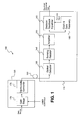
- the communication system 100 may comprise an optical communication system having an optical transmitter 120 that converts an electrical signal to an optical signal for transmission over an optical fiber network 130 to an optical receiver 110.
- the optical receiver converts the received optical signal to an electrical signal.
- the illustrated transmitter 120 includes, by way of example, one or more gain stage(s) 170 coupled to an electro-optic converter 175.
- the gain stage(s) amplify the incoming data signal and the amplified data signal in turn drives the electro-optic converter 175.
- an analog data source provides an analog data signal that modulates the output of the electro-optic converter 175.
- baseband digital modulation or frequency modulation may be used.
- the gain stage 170 may have multiple stages, and may receive one or more control signals for controlling various different parameters of the output of the electro-optic converter.
- the electro-optic converter may, for example, be a light emitting diode, a surface emitting laser or an edge emitting laser that operate at high speeds such as 10 Gigabits per second (Gbps) or higher.
- the illustrated receiver includes, by way of example, an optical detector 135, sensing resistor 140, one or more amplifier(s) 150, a clock and data recovery circuit 160, and an equalizer 165.
- the optical detector 135 can be any known prior art optical detector. Such prior art detectors convert incoming optical signals into corresponding electrical output signals that can be electronically monitored.
- One or more amplifier(s) 150 coupled to the sensing resistor amplify the sensed voltage signal.
- the amplified voltage signal drives a clock and data recovery circuit 160 that extracts a clock from the amplified voltage signal and recovers the transmitted data.
- typical high speed receivers may also include an adaptive equalizer 165, such as for example, a decision feedback equalizer that removes or reduces channel induced distortions in the received optical data.
- Decision feedback equalization techniques use feedback to cancel from the present symbol the interference from symbols which have already been detected.
- decision feedback equalization utilizes the known value of the current symbol(s) to determine and cancel the inter-symbol interference contributed by one or more prior symbol(s) in the present symbol by subtracting the previously detected symbol values with appropriate weighing.
- FIG. 2 is a simplified block diagram of a conventional one tap decision feedback equalizer 200 where a summer 210 combines incoming data 220 with a feedback signal 230.
- a slicer 240 converts the output of the summer (soft decision) to a binary signal.
- a flip flop 250 then recovers the data from the binary signal in response to an extracted clock 260.
- a multiplier 270 scales the recovered data by an equalization coefficient (g1) to generate the feedback signal 230 that is then combined with incoming data.
- the value of the equalization coefficient depends on the level of inter-symbol interference that is present in the incoming data. Typically the absolute value of the equalization coefficient (usually a negative number) increases with increasing inter-symbol interference.
- a real time optimization loop (not shown), such as a least mean square optimization loop, monitors the bit error rate of the incoming signal and adjusts the value of the equalization coefficient in response to changes in the bit error rate.
- Summer 210 then combines the equalized feedback signal 230 (typically a negative number) with the incoming data 220.
- the summer 210 therefore subtracts a scaled version of the previous symbol from a current symbol to reduce or eliminate channel induced distortion such as inter-symbol interference.
- decision feedback equalizers may not efficiently compensate for pre-cursor inter-symbol interference i.e. interference caused by symbols transmitted after the current symbol. Therefore, as illustrated in FIG. 3, current receivers 300 often include a feed-forward filter 310 and decision feedback equalizer 320 to fully compensate for both pre-cursor and post-cursor interference.
- the feed-forward filter comprises a multi-tap feed-forward equalizer with adjustable tap coefficients c 1 -c n .
- the time delay between taps may be as large as the symbol interval in which case the equalizer is a symbol-spaced equalizer.
- the equalizer is a fractionally spaced equalizer having a time delay between adjacent taps that is less than the symbol interval to avoid aliasing.
- the total delay of the feed-forward filter is typically chosen to be greater than or equal to the pre-cursor delay spread.
- the n-tap equalizer in FIG. 3 includes n multipliers 330(a)-330(n) and n-1 delay elements 340(a)-340(n-1), each of which delays a corresponding input signal by approximately one-half a symbol period.
- multipliers 330(a)-330(n) multiply the incoming data signal and delayed signals 350(a)-350(n-1) respectively by equalization coefficients c1-cn.
- Summer 360 then combines the feed forward output signals of multipliers 330(a)-330(n). The feed forward equalizer therefore subtracts scaled versions of previous symbols from a current symbol to reduce or eliminate channel induced pre-cursor inter-symbol interference.
- the output of the feed-forward equalizer is combined with the feedback signal 230 of the decision feedback equalizer.
- the decision feedback equalizer 320 functions to reduce or eliminate post-cursor inter-symbol interference as previously described with respect to FIG. 2.
- the feed forward equalizer and the decision feedback equalizer are both finite impulse response filters with adaptive coefficients that are adjusted by adaptation circuitry, such as, a least mean square calculation circuit (not shown).
- adaptation circuitry such as, a least mean square calculation circuit (not shown).
- the equalization coefficients of the feed forward equalizer and the decision feedback equalizer adapt to a filter response that matches the communication channel to reduce channel induced distortion.
- the feed forward equalizer and the decision feedback equalizer can each have any number of taps.
- the optimum number of taps is related to the amount of pulse broadening (level of distortion) incurred during transmission. Practically, higher levels of inter-symbol interference can be compensated by increasing the number of taps (i.e. the length) of the feed-forward equalizer and/or decision feedback equalizer.
- the feed forward multipliers 330(a)-330(n) consume significant die area and power as compared to the multipliers of the decision feedback equalizer.
- the decision feedback multiplier(s) is driven by a binary signal having a high or low value (i.e. one or minus one for a differential implementation). Therefore, in operation the output of the decision feedback multiplier(s) is simply the equalization coefficient or the negative value of the equalization coefficient.
- the multipliers 330(a)-330(n) of the feed forward equalizer multiply equalization coefficients c1-cn by incoming delayed analog voltage signals. The feed forward multipliers therefore require greater processing capability than the corresponding multipliers of the feedback equalizer.
- the design of a balanced receiver typically involves a tradeoff between processing complexity of the feed-forward filter and receiver sensitivity.
- the delay elements 340(a)-340(n-1) of the feed-forward filter may be implemented as dynamic sample and hold registers.
- implementations utilizing dynamic registers typically require additional clock recovery circuitry to generate n-1 extracted clock signals which can then be used to clock the delay elements 340(a)-340(n-1). Therefore, for ease of implementation, the delay cells often comprise a series of cascaded buffer stages that provide the desired delay.
- CMOS complementary metal oxide semiconductor
- each of the buffers generate inter-symbol interference that must be compensated for by the decision feedback equalizer.
- each half period delay cell should provide approximately 50ps of delay which typically requires three or more cascaded buffers each of which have a maximum of about 15-20ps of delay. Therefore a five tap 10Gbps feed forward equalizer typically needs on the order of about twelve cascaded high speed buffers.
- a receiver 400 constructed in accordance with one embodiment of the present invention may include a programmable continuous time filter 410 coupled with a decision feedback equalizer 420 to compensate for channel induced distortion in an incoming signal as illustrated in FIG. 4.
- the programmable continuous time filter 410 is an adaptive equalizer that compensates for pre-cursor distortions in the incoming signal.
- the continuous time filter 410 may serve to pre-distort the incoming signal to optimize the performance of the decision feedback equalizer.
- a bandwidth controller 430 adjusts the bandwidth of the continuous time filter 410 to tune the frequency response of the continuous time filter to approximate the inverse of at least a portion of the frequency response of the communication channel.
- FIG. 5 is a simplified block diagram of a high speed receiver 500 having an integrated continuous time filter 410 and decision feedback equalizer 420 in accordance with one embodiment of the present invention.
- the programmable continuous time filter 410 comprises one or more cascaded low pass filters 520(a-n) where the output of a first low pass filter (e.g. 520(a)) is coupled to the input of the next low pass filter (e.g. 520(b)).
- each of the low pass filters may have approximately the same frequency response.
- the bandwidth controller 430 generates, by way of example, a common control signal 430(a) that adjusts the bandwidth of each of the low pass filters 520(a-n) to reduce the level of pre-cursor ISI.
- the low pass filters 520(a-n) of the continuous time filter need not have the same frequency response. Rather, the frequency response of each of the individual filters may be unique and optimized for a particular application. In addition, the individual filters 520(a-n) need not be driven by a common control signal. Rather a real time closed loop optimizer, such as, for example, a least means square optimizer may individually adjust the bandwidth of the individual filters to compensate for the channel induced distortion.
- the low pass filters comprise, by way of example, a buffer stage with a variable capacitive load which is used to adjust the bandwidth of the device.
- FIG. 6 is a simplified circuit diagram of a single stage high speed buffer 600 for filtering the incoming data signal.
- a differential pair of inductively loaded transistors such as, for example, NMOS FETs M1 and M2 are coupled between a positive voltage source V DD and a bias current source I 1 .
- the use of inductive loads L 1 and L 2 tunes out the parasitic capacitive loading on the inputs of the buffer and increases the bandwidth of the device.
- the invention is equally applicable to single-ended or differential implementations.
- the transistors used in the low pass filter stages of the continuous time filter may or may not be the same size.
- uniformity of device size reduces process, offset, and temperature variation affects in the performance of the continuous time filter.
- NMOS FETs M1 and M2 of buffer stage 600 are driven by a complementary differential incoming signal such that when the drive signal for FET M1 is high the drive signal for FET M2 is low.
- variable capacitors C1 and C2 are coupled to the outputs of transistors M1 and M2 respectively.
- the value of variable capacitors C1 and C2 can be adjusted to compensate for pre-cursor distortions in the incoming signal or to pre-distort the incoming signal to optimize the performance of the decision feedback equalizer.
- reducing the bandwidth of the low pass filters may generate inter-symbol interference in the output signal of the continuous time filter that may then need to be compensated for by the decision feedback equalizer.
- FIG. 7 is a simplified block diagram of an exemplary bandwidth controller 430 integrated with the continuous time filter 410 and decision feedback equalizer 420 of FIG. 5.
- an analog to digital converter 710 converts the analog soft decision signal output by the summer 210 of the decision feedback equalizer to a digital signal.
- the analog to digital converter samples the analog soft decision at a relatively low rate in response to a low speed reference clock.
- the reference clock 720 may be, for example, a low-frequency signal generated by a stable oscillation source (e.g., a crystal).
- a delay lock loop (not shown) may be used to align the transition edges of the low frequency reference clock 720 with the transition edges of clock 260 which clocks the decision feedback equalizer flip flop 250 to ensure that the bandwidth controller 430 is properly synchronized with the decision feedback equalizer.
- a delay lock loop which is suitable for synchronizing the reference clock 720 and clock 260 is disclosed in commonly owned U.S. Provisional Patent Application Serial No. 60/531,095, entitled “HIGH FREQUENCY BINARY PHASE DETECTOR", filed December 19, 2003, the disclosure of which is incorporated herein by reference.
- a digital limiter 730 compares the quantized soft decision output by the analog to digital converter 710 with a threshold and generates a binary signal (e.g., one or minus one) having a low value if the quantized signal is less than the threshold and a high value if the quantized signal is greater than or equal to the threshold.
- a combiner 740 generates a bandwidth error signal 740(a) by subtracting the quantized soft decision 710(a) output by the analog to digital converter with the binary signal 730(a) output by the digital limiter.
- the bandwidth error signal 740(a) is squared and then accumulated to generate a sum square bandwidth error signal.
- an optimization algorithm may be used to reduce the value of the sum square bandwidth error signal as a function of the bandwidth of the low pass filters of the continuous time filter 410. For example, if the sum square error is reduced in response to a reduction in the bandwidth of the continuous time filter a control signal to further reduce the bandwidth of the continuous time filter is generated. Otherwise the bandwidth of the continuous time filter is increased. As discussed above in conjunction with FIG. 5, the bandwidth controller 430 then generates at least one control signal that controls the bandwidth of the continuous time filter 410.
- the continuous time filter and the decision feedback equalizer can each have any number of taps.
- the optimum number of taps is related to the amount of pulse broadening (level of distortion) incurred during transmission. Practically, higher levels of inter-symbol interference can be compensated by increasing the number of taps (i.e. the length) of the continuous time filter and or decision feedback equalizer.
- increasing the number of low pass filters in the continuous time filter increases the level of gain and improves the frequency response of the filter by decreasing the filter roll off as a function of frequency thereby reducing the level of precursor interference.
- increasing the number of filters also reduces the bandwidth of the continuous time filter with a corresponding increase in the level of inter-symbol interference created in the output of the continuous time filter.
- a high speed receiver includes a continuous time filter having six low pass filter elements integrated with a two tap decision feedback equalizer.
- the present invention is not limited to particular filter lengths. Rather the present invention may be realized with any number of low pass filters and or filter taps as may be required for a particular application.
Landscapes
- Engineering & Computer Science (AREA)
- Computer Networks & Wireless Communication (AREA)
- Signal Processing (AREA)
- Power Engineering (AREA)
- Physics & Mathematics (AREA)
- Electromagnetism (AREA)
- Cable Transmission Systems, Equalization Of Radio And Reduction Of Echo (AREA)
- Dc Digital Transmission (AREA)
Abstract
Description
According to an aspect of the invention, an optical communication device comprises:
Advantageously, the continuous time filter comprises at least one cascaded low pass filter.
Advantageously, each of the at least one low pass filter comprises a differential pair of transistors having adjustable capacitive loads coupled to outputs of the differential pair of transistors for adjusting the bandwidth of the low pass filter.
Advantageously, the decision feedback equalizer comprises a summer that generates a combined signals by combining an equalized feedback signal with the filtered incoming data signal to reduce the inter-symbol interference in the filtered incoming data signal.
Advantageously, the bandwidth controller comprises:
- an analog to digital converter, coupled to the summer, that digitizes the combined signal;
- a digital limiter, coupled to receive the digitized combined signal from the analog to digital converter, that generates a binary signal from the digitized combined signal; and
- a combiner that subtracts the digitized combined signal from the binary signal to generate a bandwidth error signal.
- a transmitter transmitting an information signal over a communication media; and
- a receiver coupled to the communication media for
receiving the transmitted information signal, wherein the
receiver comprises:
- a continuous time filter having an adjustable bandwidth, wherein the continuous time filter reduces channel induced distortion in a received information signal as a function of the adjustable bandwidth, wherein the continuous time filter generates a filtered information signal; and
- a decision feedback equalizer coupled to the continuous time filter for reducing inter-symbol interference in the filtered information signal.
Advantageously, the continuous time filter comprises at least one cascaded low pass filter.
Advantageously, each of the at least one low pass filter comprises a differential pair of transistors having adjustable capacitive loads coupled to outputs of the differential pair of transistors for adjusting the bandwidth of the low pass filter.
Advantageously, the decision feedback equalizer comprises a summer that generates a combined signal by combining an equalized feedback signal with the filtered information signal to reduce the inter-symbol interference in the filtered incoming data signal.
Advantageously, the bandwidth controller comprises:
- an analog to digital converter, coupled to the summer, that digitizes the combined signal;
- a digital limiter, coupled to receive the digitized combined signal from the analog to digital converter, that generates a binary signal from the digitized combined signal; and
- a combiner that subtracts the digitized combined signal from the binary signal to generate a bandwidth error signal.
According to an aspect of the invention, a communication system comprises:
- transmission means for transmitting an information signal over a communication media;
- receiver means coupled to the communication media for
receiving the transmitted information signal, wherein the
receiver means comprises:
- filter means for filtering the received information signal,
- bandwidth control means for adjusting the bandwidth of the filter means to reduce channel induced distortion in the received information signal, and
- equalizer means coupled to the filter means for reducing inter-symbol interference in the filtered information signal.
- filtering a first symbol of an information signal using a first filter bandwidth;
- equalizing the filtered information signal;
- generating a bandwidth error signal from at least the equalized signal; and
- filtering a second symbol of the information signal with a second filter bandwidth to reduce the bandwidth error signal.
- a continuous time filter having at least one cascaded low pass filter, each of the at least one cascaded low pass filter having an adjustable bandwidth, wherein the continuous time filter reduces channel induced distortion in an incoming data signal, wherein the continuous time filter generates a filtered incoming data signal; and
- a decision feedback equalizer coupled to the continuous time filter for reducing inter-symbol interference in the filtered incoming data signal.
Advantageously, each of the at least one low pass filter comprises a differential pair of transistors having adjustable capacitive loads coupled to outputs of the differential pair of transistors for adjusting the bandwidth of the low pass filter.
Advantageously, the decision feedback equalizer comprises a summer that combines an equalized feedback signal with the filtered incoming data signal to reduce the inter-symbol interference in the filtered incoming data signal.
Advantageously, the bandwidth controller comprises:
- an analog to digital converter, coupled to the summer, that digitizes the combined signal;
- a digital limiter, coupled to receive the digitized combined signal from the analog to digital converter, that generates a binary signal from the digitized combined signal; and
- a combiner that subtracts the digitized combined signal from the binary signal to generate a bandwidth error signal.
Claims (10)
- An optical communication device comprising:a continuous time filter having an adjustable bandwidth, wherein the continuous time filter reduces channel induced distortion in an incoming data signal, wherein the continuous time filter generates a filtered incoming data signal; anda decision feedback equalizer, coupled to the continuous time filter, for reducing inter-symbol interference in the filtered incoming data signal.
- The communication device of claim 1 further comprising a bandwidth controller that estimates bandwidth error of the continuous time filter and generates a control signal to adjust the bandwidth of the continuous time filter to reduce the bandwidth error.
- The communication device of claim 1 wherein the continuous time filter comprises at least one cascaded low pass filter.
- The communication device of claim 3 wherein each of the at least one low pass filter comprises a differential pair of transistors having adjustable capacitive loads coupled to outputs of the differential pair of transistors for adjusting the bandwidth of the low pass filter.
- A communication system comprising:a transmitter transmitting an information signal over a communication media; anda receiver coupled to the communication media for receiving the transmitted information signal, wherein the receiver comprises:a continuous time filter having an adjustable bandwidth, wherein the continuous time filter reduces channel induced distortion in a received information signal as a function of the adjustable bandwidth, wherein the continuous time filter generates a filtered information signal; anda decision feedback equalizer coupled to the continuous time filter for reducing inter-symbol interference in the filtered information signal.
- The communication system of claim 5 further comprising a bandwidth controller that estimates bandwidth error of the continuous time filter and generates a control signal to adjust the bandwidth of the continuous time filter to reduce the bandwidth error
- A communication system comprising:transmission means for transmitting an information signal over a communication media;receiver means coupled to the communication media for receiving the transmitted information signal, wherein the receiver means comprises:filter means for filtering the received information signal,bandwidth control means for adjusting the bandwidth of the filter means to reduce channel induced distortion in the received information signal, andequalizer means coupled to the filter means for reducing inter-symbol interference in the filtered information signal.
- A method for communicating an information signal, comprising:filtering a first symbol of an information signal using a first filter bandwidth;equalizing the filtered information signal;generating a bandwidth error signal from at least the equalized signal; andfiltering a second symbol of the information signal with a second filter bandwidth to reduce the bandwidth error signal.
- An optical communication device comprising:a continuous time filter having at least one cascaded low pass filter, each of the at least one cascaded low pass filter having an adjustable bandwidth, wherein the continuous time filter reduces channel induced distortion in an incoming data signal, wherein the continuous time filter generates a filtered incoming data signal; anda decision feedback equalizer coupled to the continuous time filter for reducing inter-symbol interference in the filtered incoming data signal.
- The communication device of claim 9 further comprising a bandwidth controller that estimates bandwidth error of the continuous time filter and generates at least one control signal to adjust the bandwidth of the at least one cascaded low pass filter to reduce the bandwidth error.
Applications Claiming Priority (8)
| Application Number | Priority Date | Filing Date | Title |
|---|---|---|---|
| US774724 | 1985-09-11 | ||
| US53140303P | 2003-12-19 | 2003-12-19 | |
| US53140203P | 2003-12-19 | 2003-12-19 | |
| US53096803P | 2003-12-19 | 2003-12-19 | |
| US530968P | 2003-12-19 | ||
| US531403P | 2003-12-19 | ||
| US531402P | 2003-12-19 | ||
| US10/774,724 US7522847B2 (en) | 2003-12-19 | 2004-02-09 | Continuous time filter-decision feedback equalizer architecture for optical channel equalization |
Publications (3)
| Publication Number | Publication Date |
|---|---|
| EP1545030A2 true EP1545030A2 (en) | 2005-06-22 |
| EP1545030A3 EP1545030A3 (en) | 2008-02-13 |
| EP1545030B1 EP1545030B1 (en) | 2012-09-19 |
Family
ID=34528252
Family Applications (1)
| Application Number | Title | Priority Date | Filing Date |
|---|---|---|---|
| EP04026611A Expired - Lifetime EP1545030B1 (en) | 2003-12-19 | 2004-11-09 | Optical channel equalisation |
Country Status (4)
| Country | Link |
|---|---|
| US (1) | US7522847B2 (en) |
| EP (1) | EP1545030B1 (en) |
| CN (1) | CN1655483B (en) |
| TW (1) | TWI259667B (en) |
Cited By (3)
| Publication number | Priority date | Publication date | Assignee | Title |
|---|---|---|---|---|
| EP1788734A1 (en) * | 2005-11-21 | 2007-05-23 | Alcatel Lucent | Method of transmitting an optical signal and transmission system |
| US8824540B2 (en) | 2012-08-22 | 2014-09-02 | International Business Machines Corporation | Decision feedback equalizers with high-order continuous time feedback |
| WO2019167275A1 (en) * | 2018-03-02 | 2019-09-06 | 株式会社日立製作所 | Decision feedback equalizer and receiver using same |
Families Citing this family (34)
| Publication number | Priority date | Publication date | Assignee | Title |
|---|---|---|---|---|
| US7822113B2 (en) * | 2003-12-19 | 2010-10-26 | Broadcom Corporation | Integrated decision feedback equalizer and clock and data recovery |
| US7623600B2 (en) | 2004-06-02 | 2009-11-24 | Broadcom Corporation | High speed receive equalizer architecture |
| US7697603B1 (en) * | 2004-10-18 | 2010-04-13 | Altera Corporation | Methods and apparatus for equalization in high-speed backplane data communication |
| US7236550B1 (en) * | 2004-11-01 | 2007-06-26 | Synopsys, Inc. | Method and apparatus for tail cancellation equalization |
| US8111986B1 (en) | 2004-12-22 | 2012-02-07 | Clariphy Communications, Inc. | Testing of transmitters for communication links by software simulation of reference channel and/or reference receiver |
| US7924910B2 (en) * | 2005-01-04 | 2011-04-12 | Vitesse Semiconductor Corporation | Adaptive equalization with group delay |
| US7853149B2 (en) * | 2005-03-08 | 2010-12-14 | Clariphy Communications, Inc. | Transmitter frequency peaking for optical fiber channels |
| ATE434299T1 (en) * | 2005-10-27 | 2009-07-15 | Alcatel Lucent | DEVICE FOR ADAPTIVE EQUALIZATION OF AN OPTICAL POLARIZATION ENCRYPTED SIGNAL |
| US8054876B2 (en) * | 2005-12-13 | 2011-11-08 | Infinera Corporation | Active delay line |
| WO2007114944A2 (en) | 2006-04-04 | 2007-10-11 | Rambus, Inc. | Phase control block for managing multiple clock domains in systems with frequency offsets |
| CN101207445A (en) * | 2006-12-21 | 2008-06-25 | 华为技术有限公司 | A dispersion compensation method and optical fiber transmission system |
| US8548110B2 (en) * | 2007-01-09 | 2013-10-01 | Rambus Inc. | Receiver with clock recovery circuit and adaptive sample and equalizer timing |
| US7983333B2 (en) | 2007-02-09 | 2011-07-19 | Broadcom Corporation | Non-linear analog decision feedback equalizer |
| US7869780B2 (en) * | 2007-04-19 | 2011-01-11 | Skyworks Solutions, Inc. | Phase-locked loop based controller for adjusting an adaptive continuous-time filter |
| JP4924276B2 (en) * | 2007-08-06 | 2012-04-25 | 住友電気工業株式会社 | Distributed equalization method, distributed equalization apparatus, and optical transceiver |
| US8989214B2 (en) * | 2007-12-17 | 2015-03-24 | Altera Corporation | High-speed serial data signal receiver circuitry |
| US8170829B1 (en) * | 2008-03-24 | 2012-05-01 | Cisco Technology, Inc. | Tester bundle |
| US7872823B2 (en) * | 2009-01-12 | 2011-01-18 | Lsi Corporation | AGC loop with weighted zero forcing and LMS error sources and methods for using such |
| US8675724B2 (en) | 2009-10-20 | 2014-03-18 | Taiwan Semiconductor Manufacturing Company, Ltd. | Decision feedback equalizers and operating methods thereof |
| CN102204132B (en) * | 2009-12-15 | 2014-10-15 | 穆尔蒂菲有限公司 | Method and system for coherently equalizing chromatic dispersion of an optical signal in an optical fiber |
| US8879616B2 (en) | 2011-10-31 | 2014-11-04 | Hewlett-Packard Development Company, L.P. | Receiver with decision feedback equalizer |
| US8963573B2 (en) | 2011-12-22 | 2015-02-24 | Cisco Technology, Inc. | Universal test system for testing electrical and optical hosts |
| US9025575B2 (en) | 2012-11-15 | 2015-05-05 | Telefonaktiebolaget Lm Ericsson (Publ) | Antenna array calibration using traffic signals |
| US10116389B2 (en) * | 2014-06-10 | 2018-10-30 | Telefonaktiebolaget Lm Ericsson (Publ) | Optical transceiver |
| CN107925641B (en) | 2015-10-15 | 2021-05-07 | 拉姆伯斯公司 | PAM-4DFE Architecture with DFE Tap Values Dependent on Sign Conversion |
| US10715261B2 (en) | 2016-05-24 | 2020-07-14 | Telefonaktiebolaget Lm Ericsson (Publ) | Method and apparatus for antenna array calibration using on-board receiver |
| CN106301229B (en) * | 2016-08-17 | 2018-12-14 | 灿芯半导体(上海)有限公司 | Data receiver circuit |
| US10496309B2 (en) * | 2016-11-13 | 2019-12-03 | Intel Corporation | Input/output (I/O) loopback function for I/O signaling testing |
| EP3679664B1 (en) | 2017-09-06 | 2021-11-03 | Telefonaktiebolaget LM Ericsson (publ) | Method and apparatus for antenna array calibration with interference reduction |
| EP3704820B1 (en) | 2017-10-31 | 2022-04-27 | Telefonaktiebolaget LM Ericsson (publ) | Orthogonal training signals for transmission in an antenna array |
| US20200076510A1 (en) * | 2018-08-30 | 2020-03-05 | Oe Solutions America, Inc. | Method and apparatus for designing matching network for eam for eml tosa |
| US20200162172A1 (en) * | 2018-11-21 | 2020-05-21 | Ciena Corporation | Physical-Layer Security for Coherent Communications System |
| CN113779744B (en) * | 2020-06-10 | 2023-07-18 | 英业达科技有限公司 | Method for determining continuous time linear equalizer settings |
| TWI763459B (en) * | 2021-04-23 | 2022-05-01 | 瑞昱半導體股份有限公司 | Switch device and signal adjusting method thereof |
Citations (2)
| Publication number | Priority date | Publication date | Assignee | Title |
|---|---|---|---|---|
| EP0808046A2 (en) | 1996-05-16 | 1997-11-19 | Symbios Logic Inc. | Digital signal processing apparatus and method |
| US5940441A (en) | 1996-10-29 | 1999-08-17 | International Business Machines Corporation | Integrated adaptive cable equalizer using a continuous-time filter |
Family Cites Families (18)
| Publication number | Priority date | Publication date | Assignee | Title |
|---|---|---|---|---|
| US5179302A (en) * | 1991-04-03 | 1993-01-12 | Loral Aerospace Corp. | Tunable data filter |
| US5671252A (en) * | 1994-09-21 | 1997-09-23 | Analog Devices, Inc. | Sampled data read channel utilizing charge-coupled devices |
| US5774505A (en) * | 1996-04-04 | 1998-06-30 | Hewlett-Packard Company | Intersymbol interference cancellation with reduced complexity |
| US6069522A (en) * | 1997-02-03 | 2000-05-30 | Texas Instruments Incorporated | Circuitry and method for providing boost and asymmetry in a continuous-time filter |
| US6285709B1 (en) * | 1997-10-31 | 2001-09-04 | 3 Com Corporation | Error filtering in a hybrid equalizer system |
| US6144697A (en) * | 1998-02-02 | 2000-11-07 | Purdue Research Foundation | Equalization techniques to reduce intersymbol interference |
| US6233107B1 (en) * | 1998-03-20 | 2001-05-15 | Seagate Technology Llc | Analog self-synchronization subsystem based on peak detection and post processing in a sampled channel of digital magnetic recording |
| GB9916907D0 (en) * | 1999-07-19 | 1999-09-22 | Cambridge Silicon Radio Ltd | Variable oscillator |
| US6968167B1 (en) * | 1999-10-21 | 2005-11-22 | Broadcom Corporation | Adaptive radio transceiver with calibration |
| ATE410842T1 (en) | 2000-07-21 | 2008-10-15 | Broadcom Corp | METHOD AND SYSTEM FOR DIGITAL PROCESSING OF OPTICAL DATA SIGNALS |
| US7054606B1 (en) * | 2001-09-21 | 2006-05-30 | Lsi Logic Corporation | Digitally calibrated narrowband filter with analog channel compensation |
| US7353245B2 (en) * | 2002-09-04 | 2008-04-01 | Agere Systems Inc. | Adaptive filter coefficient determination |
| US7830956B2 (en) * | 2003-02-05 | 2010-11-09 | Fujitsu Limited | Method and system for processing a sampled signal |
| US7016406B1 (en) * | 2003-04-29 | 2006-03-21 | Scintera Networks | Adaptation structure and methods for analog continuous time equalizers |
| US7471904B2 (en) * | 2003-07-25 | 2008-12-30 | Alcatel-Lucent Usa Inc. | Method and apparatus for electronic equalization in optical communication systems |
| TW589785B (en) * | 2003-08-01 | 2004-06-01 | Winbond Electronics Corp | Digitally controlled tuner circuit |
| US7302461B2 (en) * | 2003-11-26 | 2007-11-27 | Scintera Networks, Inc. | Analog delay elements |
| US7272178B2 (en) * | 2003-12-08 | 2007-09-18 | Freescale Semiconductor, Inc. | Method and apparatus for controlling the bandwidth frequency of an analog filter |
-
2004
- 2004-02-09 US US10/774,724 patent/US7522847B2/en not_active Expired - Fee Related
- 2004-11-09 EP EP04026611A patent/EP1545030B1/en not_active Expired - Lifetime
- 2004-12-10 TW TW093138406A patent/TWI259667B/en not_active IP Right Cessation
- 2004-12-13 CN CN2004101040623A patent/CN1655483B/en not_active Expired - Fee Related
Patent Citations (2)
| Publication number | Priority date | Publication date | Assignee | Title |
|---|---|---|---|---|
| EP0808046A2 (en) | 1996-05-16 | 1997-11-19 | Symbios Logic Inc. | Digital signal processing apparatus and method |
| US5940441A (en) | 1996-10-29 | 1999-08-17 | International Business Machines Corporation | Integrated adaptive cable equalizer using a continuous-time filter |
Cited By (4)
| Publication number | Priority date | Publication date | Assignee | Title |
|---|---|---|---|---|
| EP1788734A1 (en) * | 2005-11-21 | 2007-05-23 | Alcatel Lucent | Method of transmitting an optical signal and transmission system |
| US8824540B2 (en) | 2012-08-22 | 2014-09-02 | International Business Machines Corporation | Decision feedback equalizers with high-order continuous time feedback |
| US8842722B2 (en) | 2012-08-22 | 2014-09-23 | International Business Machines Corporation | Decision feedback equalizers with high-order continuous time feedback |
| WO2019167275A1 (en) * | 2018-03-02 | 2019-09-06 | 株式会社日立製作所 | Decision feedback equalizer and receiver using same |
Also Published As
| Publication number | Publication date |
|---|---|
| TWI259667B (en) | 2006-08-01 |
| TW200541235A (en) | 2005-12-16 |
| EP1545030B1 (en) | 2012-09-19 |
| US20050135475A1 (en) | 2005-06-23 |
| EP1545030A3 (en) | 2008-02-13 |
| CN1655483A (en) | 2005-08-17 |
| US7522847B2 (en) | 2009-04-21 |
| CN1655483B (en) | 2012-07-25 |
Similar Documents
| Publication | Publication Date | Title |
|---|---|---|
| EP1545030B1 (en) | Optical channel equalisation | |
| US7974337B2 (en) | High speed receive equalizer architecture | |
| EP1545043B1 (en) | Using clock and data recovery phase adjust to set loop delay of a decision feedback equalizer | |
| US8831142B2 (en) | Adaptive cancellation of voltage offset in a communication system | |
| US8964825B2 (en) | Analog signal current integrators with tunable peaking function | |
| US20150381393A1 (en) | Adaptive Cancellation of Voltage Offset in a Communication System | |
| US7130366B2 (en) | Compensation circuit and method for reducing intersymbol interference products caused by signal transmission via dispersive media | |
| US7471904B2 (en) | Method and apparatus for electronic equalization in optical communication systems | |
| US8385401B2 (en) | Equalizer and method for performing equalization | |
| CN110858824B (en) | Pre-compensator based quantization for clock recovery | |
| US8054876B2 (en) | Active delay line | |
| US20040012433A1 (en) | Adaptive noise filtering and equalization for optimal high speed multilevel signal decoding | |
| US20150110165A1 (en) | Transmitter Training Using Receiver Equalizer Coefficients | |
| US20120027418A1 (en) | Equalizer for an Optical Transmission System | |
| US7436882B2 (en) | Decision feedback equalizer and clock and data recovery circuit for high speed applications | |
| EP1545044B1 (en) | Decision feedback equalizer and clock and data recovery circuit for high-speed applications | |
| US7293057B2 (en) | Method and apparatus for cancelling inter-symbol interference (ISI) within a communication channel | |
| US20050254569A1 (en) | System and method for generating equalization coefficients | |
| US20020084870A1 (en) | Programmable driver/equalizer with alterable anlog finite impulse response (FIR) filter having low intersymbol interference & constant peak amplitude independent of coefficient settings | |
| CN114208065B (en) | Noise cancellation apparatus and method for receiver | |
| Carusone | Practical Challenges for Electronic Dispersion Compensation in CMOS | |
| WO2020064780A1 (en) | Cascadable filter architecture | |
| WO2003088478A1 (en) | Compensation circuit and method for reducing intersymbol interference products caused by signal transmission via dispersive media |
Legal Events
| Date | Code | Title | Description |
|---|---|---|---|
| PUAI | Public reference made under article 153(3) epc to a published international application that has entered the european phase |
Free format text: ORIGINAL CODE: 0009012 |
|
| AK | Designated contracting states |
Kind code of ref document: A2 Designated state(s): AT BE BG CH CY CZ DE DK EE ES FI FR GB GR HU IE IS IT LI LU MC NL PL PT RO SE SI SK TR |
|
| AX | Request for extension of the european patent |
Extension state: AL HR LT LV MK YU |
|
| RAP1 | Party data changed (applicant data changed or rights of an application transferred) |
Owner name: BROADCOM CORPORATION |
|
| PUAL | Search report despatched |
Free format text: ORIGINAL CODE: 0009013 |
|
| AK | Designated contracting states |
Kind code of ref document: A3 Designated state(s): AT BE BG CH CY CZ DE DK EE ES FI FR GB GR HU IE IS IT LI LU MC NL PL PT RO SE SI SK TR |
|
| AX | Request for extension of the european patent |
Extension state: AL HR LT LV MK YU |
|
| RIC1 | Information provided on ipc code assigned before grant |
Ipc: H04L 25/03 20060101ALI20080104BHEP Ipc: H04B 10/158 20060101AFI20080104BHEP |
|
| 17P | Request for examination filed |
Effective date: 20080813 |
|
| AKX | Designation fees paid |
Designated state(s): DE FR GB |
|
| 17Q | First examination report despatched |
Effective date: 20090514 |
|
| GRAP | Despatch of communication of intention to grant a patent |
Free format text: ORIGINAL CODE: EPIDOSNIGR1 |
|
| GRAS | Grant fee paid |
Free format text: ORIGINAL CODE: EPIDOSNIGR3 |
|
| GRAA | (expected) grant |
Free format text: ORIGINAL CODE: 0009210 |
|
| AK | Designated contracting states |
Kind code of ref document: B1 Designated state(s): DE FR GB |
|
| REG | Reference to a national code |
Ref country code: GB Ref legal event code: FG4D Ref country code: DE Ref legal event code: R081 Ref document number: 602004039347 Country of ref document: DE Owner name: AVAGO TECHNOLOGIES GENERAL IP (SINGAPORE) PTE., SG Free format text: FORMER OWNER: BROADCOM CORP., IRVINE, CALIF., US |
|
| REG | Reference to a national code |
Ref country code: DE Ref legal event code: R096 Ref document number: 602004039347 Country of ref document: DE Effective date: 20121115 |
|
| PLBE | No opposition filed within time limit |
Free format text: ORIGINAL CODE: 0009261 |
|
| STAA | Information on the status of an ep patent application or granted ep patent |
Free format text: STATUS: NO OPPOSITION FILED WITHIN TIME LIMIT |
|
| 26N | No opposition filed |
Effective date: 20130620 |
|
| REG | Reference to a national code |
Ref country code: DE Ref legal event code: R097 Ref document number: 602004039347 Country of ref document: DE Effective date: 20130620 |
|
| REG | Reference to a national code |
Ref country code: FR Ref legal event code: PLFP Year of fee payment: 12 |
|
| REG | Reference to a national code |
Ref country code: FR Ref legal event code: PLFP Year of fee payment: 13 |
|
| PGFP | Annual fee paid to national office [announced via postgrant information from national office to epo] |
Ref country code: GB Payment date: 20161128 Year of fee payment: 13 Ref country code: FR Payment date: 20161123 Year of fee payment: 13 |
|
| REG | Reference to a national code |
Ref country code: DE Ref legal event code: R082 Ref document number: 602004039347 Country of ref document: DE Representative=s name: BOSCH JEHLE PATENTANWALTSGESELLSCHAFT MBH, DE Ref country code: DE Ref legal event code: R081 Ref document number: 602004039347 Country of ref document: DE Owner name: AVAGO TECHNOLOGIES INTERNATIONAL SALES PTE. LT, SG Free format text: FORMER OWNER: BROADCOM CORPORATION, IRVINE, CALIF., US Ref country code: DE Ref legal event code: R081 Ref document number: 602004039347 Country of ref document: DE Owner name: AVAGO TECHNOLOGIES GENERAL IP (SINGAPORE) PTE., SG Free format text: FORMER OWNER: BROADCOM CORPORATION, IRVINE, CALIF., US |
|
| REG | Reference to a national code |
Ref country code: GB Ref legal event code: 732E Free format text: REGISTERED BETWEEN 20171005 AND 20171011 |
|
| REG | Reference to a national code |
Ref country code: FR Ref legal event code: TP Owner name: AVAGO TECHNOLOGIES GENERAL IP PTE. LTD., SG Effective date: 20180228 |
|
| GBPC | Gb: european patent ceased through non-payment of renewal fee |
Effective date: 20171109 |
|
| REG | Reference to a national code |
Ref country code: FR Ref legal event code: ST Effective date: 20180731 |
|
| REG | Reference to a national code |
Ref country code: DE Ref legal event code: R082 Ref document number: 602004039347 Country of ref document: DE Representative=s name: BOSCH JEHLE PATENTANWALTSGESELLSCHAFT MBH, DE Ref country code: DE Ref legal event code: R081 Ref document number: 602004039347 Country of ref document: DE Owner name: AVAGO TECHNOLOGIES INTERNATIONAL SALES PTE. LT, SG Free format text: FORMER OWNER: AVAGO TECHNOLOGIES GENERAL IP (SINGAPORE) PTE. LTD., SINGAPORE, SG |
|
| PG25 | Lapsed in a contracting state [announced via postgrant information from national office to epo] |
Ref country code: FR Free format text: LAPSE BECAUSE OF NON-PAYMENT OF DUE FEES Effective date: 20171130 |
|
| PG25 | Lapsed in a contracting state [announced via postgrant information from national office to epo] |
Ref country code: GB Free format text: LAPSE BECAUSE OF NON-PAYMENT OF DUE FEES Effective date: 20171109 |
|
| PGFP | Annual fee paid to national office [announced via postgrant information from national office to epo] |
Ref country code: DE Payment date: 20211110 Year of fee payment: 18 |
|
| REG | Reference to a national code |
Ref country code: DE Ref legal event code: R119 Ref document number: 602004039347 Country of ref document: DE |
|
| PG25 | Lapsed in a contracting state [announced via postgrant information from national office to epo] |
Ref country code: DE Free format text: LAPSE BECAUSE OF NON-PAYMENT OF DUE FEES Effective date: 20230601 |