EP1544941A1 - Angepasstes veränderbares Mikrowellendämpfungsglied - Google Patents
Angepasstes veränderbares Mikrowellendämpfungsglied Download PDFInfo
- Publication number
- EP1544941A1 EP1544941A1 EP03425804A EP03425804A EP1544941A1 EP 1544941 A1 EP1544941 A1 EP 1544941A1 EP 03425804 A EP03425804 A EP 03425804A EP 03425804 A EP03425804 A EP 03425804A EP 1544941 A1 EP1544941 A1 EP 1544941A1
- Authority
- EP
- European Patent Office
- Prior art keywords
- line section
- lin1
- lin2
- line
- attenuator
- Prior art date
- Legal status (The legal status is an assumption and is not a legal conclusion. Google has not performed a legal analysis and makes no representation as to the accuracy of the status listed.)
- Granted
Links
- 239000000758 substrate Substances 0.000 abstract description 8
- 230000005540 biological transmission Effects 0.000 abstract description 7
- 101000922137 Homo sapiens Peripheral plasma membrane protein CASK Proteins 0.000 description 13
- 102100031166 Peripheral plasma membrane protein CASK Human genes 0.000 description 13
- 102100027206 CD2 antigen cytoplasmic tail-binding protein 2 Human genes 0.000 description 10
- 101000914505 Homo sapiens CD2 antigen cytoplasmic tail-binding protein 2 Proteins 0.000 description 10
- 239000011159 matrix material Substances 0.000 description 10
- 238000003780 insertion Methods 0.000 description 6
- 230000037431 insertion Effects 0.000 description 6
- 210000004027 cell Anatomy 0.000 description 3
- 230000009466 transformation Effects 0.000 description 3
- 230000006978 adaptation Effects 0.000 description 2
- PNEYBMLMFCGWSK-UHFFFAOYSA-N aluminium oxide Inorganic materials [O-2].[O-2].[O-2].[Al+3].[Al+3] PNEYBMLMFCGWSK-UHFFFAOYSA-N 0.000 description 2
- 239000003990 capacitor Substances 0.000 description 2
- 230000000694 effects Effects 0.000 description 2
- 210000001744 T-lymphocyte Anatomy 0.000 description 1
- 230000007423 decrease Effects 0.000 description 1
- 230000003247 decreasing effect Effects 0.000 description 1
- 230000009977 dual effect Effects 0.000 description 1
- 238000005516 engineering process Methods 0.000 description 1
- 238000002955 isolation Methods 0.000 description 1
- 238000004519 manufacturing process Methods 0.000 description 1
- 230000007246 mechanism Effects 0.000 description 1
- 229910052751 metal Inorganic materials 0.000 description 1
- 239000002184 metal Substances 0.000 description 1
- 150000002739 metals Chemical class 0.000 description 1
- 238000000034 method Methods 0.000 description 1
- 230000004224 protection Effects 0.000 description 1
- 230000004044 response Effects 0.000 description 1
- 238000004544 sputter deposition Methods 0.000 description 1
Images

Classifications
-
- H—ELECTRICITY
- H01—ELECTRIC ELEMENTS
- H01P—WAVEGUIDES; RESONATORS, LINES, OR OTHER DEVICES OF THE WAVEGUIDE TYPE
- H01P1/00—Auxiliary devices
- H01P1/22—Attenuating devices
- H01P1/227—Strip line attenuators
Definitions
- the present invention relates to the field of microwave attenuator and more precisely to a matched microwave variable attenuator.
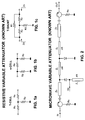
- Variable microwave attenuators based on pin diodes are well known in the art. These attenuators are derivable from canonical resistive structures such as the one depicted in Figure 1a , 1b , and 1c , for T -cell, ⁇ -cell, and T-shunt cell, respectively. Dual-port circuits of fig.1a and 1c can be mathematically described by an impedance matrix of the type: where: R 11 is the resistance seen at the 1-1 port, while R 21 is the 2 ⁇ 1 transfer resistances. Similar remarks, of course, apply to elements R 22 and R 12 .
- R G and R L the internal resistance of the generator and the load
- the maximum transfer of power from the generator to the load also corresponding to the minimum attenuation, takes place when R G and R L are matched to the resistance seen at the respective ports.
- Resistive attenuator starts attenuating as the match condition is left out.
- the desired attenuation is achieved by opportunely dimensioning the elements of the resistance matrix.
- a microwave variable attenuator is obtainable in line of principle by replacing one or more the resistances of the resistive attenuators with pin diodes having a resistance decreasing with the increase of the DC bias current flowing through them.
- pin diodes include unwanted reactive elements, such as: junction capacitance, case capacitance, and chip-to-case connection inductance, which limit their performances and call for an optimisation of the design inside the operation band.
- Two-port network including both dissipative and reactive elements are modelled by an impedance matrix Z whose elements [ z x , y ] include both resistance and reactance components, or by an admittance matrix Y whose elements [ y x,y ] include both admittance ad susceptance components.
- the unwanted reactive elements namely reactance or susceptance, limit the maximum attenuation (decoupling) on serial branches of the attenuator, whereas they increase the insertion loss on parallel branches.
- S scattering matrix
- apex - and + indicate signals outgoing from or incoming to two transmission lines respectively connected to the ports indicated by subscript 1 and 2 .
- S 11 is the reflection coefficient in the input line
- S 21 is the transmission coefficient into output line from input line. Similar remarks, of course, apply to elements S 22 and S 12 .
- the microwave attenuators described by matrix S can also attenuate by exploiting the mechanism of reflecting the waves towards the input port due to the various unmatching condition along the propagation path. In the latter case the attenuation can take place without or with partial power dissipation in the load.
- Preferred embodiments of pin diode attenuators are the ones having large attenuations and low insertion losses.
- the latter being defined as the ratio between the power delivered to the load before and after the insertion of the attenuator driven for null attenuation.
- the requisite of low insertion loss cannot leave out of consideration the frequency response of the microwave attenuators. In order to reach greater attenuations more attenuation cells can be cascaded to each other.
- the attenuator includes a configuration having two contiguous ⁇ /4 microstrip lines with characteristic impedance of Z T serially connected at the two ends with two respective microstrips of Z O , in their turn connected to the input and output ports of the attenuator.
- the anode of a first pin diode is connected between the ⁇ /4 microstrips while the cathode is grounded.
- the cathode of a second pin diode is connected between the two microstrips of different impedance, while the anode is connected to a third ⁇ /4 microstrip whose impedance is less than Z O .
- the two diodes are serially biased so that their resistances are the same.
- the attenuator of fig.2 seems to be inspired to some golden technical rules to achieve good designs with pin diode attenuators, in particular:
- the major drawback of the attenuator of the cited invention is that to be disadapted (unmatched) both at the input and the output ports, so that two circulators are needed, or equivalent devices, such as hybrids employed with balanced structures. Circulators and hybrids have manufacturing costs comparable if not greater than the cost of the attenuator. Furthermore the area of the complete circuit on the dielectric substrate is noticeable increased to the detriment of miniaturization requirements.
- microwave variable attenuators including pin diodes
- the main object of the present invention is that to indicate an alternative structure able to perform prevalently dissipative attenuation keeping the adaptation at both the input and output ports unchanged for all the values of the variable attenuation, without additional circulators, hybrids, or similar devices are needed.
- the invention achieves said object by providing a variable microwave attenuator, as disclosed in claim 1.
- variable attenuator consists of a dielectric substrate which supports a microstrip layout plus some discrete components mounted on it, including:
- the two line sections are parallel straight-lines.
- a ring configuration of the microstrip layout according to a second preferred embodiment allows to reduce the occupied surface on the substrate and increase the decoupling between the microstrips.
- the two pin diodes are serially biased to set equal values of their resistances.
- the one of the invention keeps as far as possible constant the adaptation at the input and output ports during the whole attenuation range. In any case, quite a different structure is disclosed indeed.
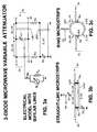
- an electrical model of the attenuator includes a first bifilar line LIN1 connected between the input and the output ports, and a second bifilar line LIN2 visible under the first one.
- the input and the output ports are not specifically indicated because the attenuator is symmetric.
- the two bifilar lines are unbalanced, having a wire connected to the ground.
- the second bifilar line LIN2 is ⁇ /2 long and presents a characteristic impedance Z, whose value is indifferent for the aim of the invention.
- the cathode of the second diode is connected to ground, while the anode is connected to the line LIN2, in such a way the second pin diode results biased in series with the first one.
- the series of the two pin diodes is fed by a current Idc, injected into the anode of the first diode by a current generator A l .
- a first microstrip embodiment of the electrical model of the attenuator of the preceding figure is shown.
- the metallic layout of the upper face of a dielectric alumina substrate is depicted.
- the bottom face of the substrate includes a metallized ground plane in correspondence of the upper layout for achieving microstrip lines.
- the metallic layout is lay down by means of well consolidated methods, for example sputtering.
- the thickness and the width of the lines LIN1 and LIN2 are calculated for obtaining the desired characteristic impedances Z O and Z, respectively. Connections to the ground plane are performed by metallized through holes.
- Elements other than microstrips are connected by advantageously employing known tools of the surface mount technology.
- the two resistors R O can be manufactured by laying down resistive metals.
- a second microstrip embodiment of the electrical model depicted in fig.3a is shown.
- the second embodiment differs from the preceding one by the only different shape of the metallic layout which is circular instead of rectangular but the electrical behaviour is the same.
- the ring configuration allows to save space on the upper face of the substrate of alumina.
- the inventors' intuitions of above have been taken into duly consideration to develop a design for obtaining the circuital structure (unknown) of a variable microwave attenuator.
- R1* R2
- the inventors have decided to act on the serial branch R1 of the T-shunt attenuator, maintaining as far as possible the equivalence of the remaining part. This choice is motivated by the fact of trying to remove the pin diode from the serial branch, according to the arguments raised in the introduction. Because of the symmetry of the T-shunt attenuator, two quarter wave line sections and a resistance Zo 2 / R2 shall be used, as shown in the upper part of fig.3b .
- Equality (7b) is valid on condition that the electrical equivalence during the passage from the purely resistive T-shunt of fig.1c to the microwave attenuator of fig.3b is kept unchanged. During this passage the effect of the phase offset of the signal across the various branches must be taken into account.
- the RF signal coming to the attenuator is split in two signals, a first one travels along the two contiguous ⁇ /4 tracts undergoing a ⁇ /2 phase offset at the output of the attenuator, the second one crosses the two resistors and leaves the attenuator with a phase offset which depends on the electrical length of the connection.
- Most critic conditions occur in case the two diodes are interrupted and R1*, R2 tend to ⁇ .
- a line section having an electrical length of ⁇ /2 shall be inserted in series with the two resistances Ro. This prevents the two resistors Ro being crossed by a current when the two diodes are interrupted, or a very low attenuation is set. In fact, phase offset across two whatever paths departing from the input and joining at the output of the attenuator is the same, in this circumstance the two ends of each resistor Ro are equipotential and the current is null. Furthermore, the insertion of the ⁇ /2 line section does not compromise the behaviour of the network.
- a ⁇ /2 transmission line has the property of reporting the impedance present at one end to the other end unchanged, independently of its characteristic impedance. The property is made immediately perceptible on the Smith's chart, where a ⁇ /2 impedance transformation corresponds to a complete turn terminating in the starting point.
- both the embodiments of figures 3b and 3c include microstrips LIN1 and LIN2 equal to each other; that is with the same electrical length and the same dimensional length, in this case the characteristic impedance Z of the microstrip LIN2 is equal to Zo of course. But this is not the rule because embodiments with LIN1 and LIN2 of the same electrical ⁇ /2 length and different dimensional lengths are possible; obviously, different shapes of the layout are resulting.
Landscapes
- Non-Reversible Transmitting Devices (AREA)
- Attenuators (AREA)
- Control Of Motors That Do Not Use Commutators (AREA)
- Toilet Supplies (AREA)
Priority Applications (3)
| Application Number | Priority Date | Filing Date | Title |
|---|---|---|---|
| EP03425804A EP1544941B1 (de) | 2003-12-17 | 2003-12-17 | Angepasstes veränderbares Mikrowellendämpfungsglied |
| DE60320271T DE60320271T2 (de) | 2003-12-17 | 2003-12-17 | Angepasstes veränderbares Mikrowellendämpfungsglied |
| AT03425804T ATE392022T1 (de) | 2003-12-17 | 2003-12-17 | Angepasstes veränderbares mikrowellendämpfungsglied |
Applications Claiming Priority (1)
| Application Number | Priority Date | Filing Date | Title |
|---|---|---|---|
| EP03425804A EP1544941B1 (de) | 2003-12-17 | 2003-12-17 | Angepasstes veränderbares Mikrowellendämpfungsglied |
Publications (2)
| Publication Number | Publication Date |
|---|---|
| EP1544941A1 true EP1544941A1 (de) | 2005-06-22 |
| EP1544941B1 EP1544941B1 (de) | 2008-04-09 |
Family
ID=34486569
Family Applications (1)
| Application Number | Title | Priority Date | Filing Date |
|---|---|---|---|
| EP03425804A Expired - Lifetime EP1544941B1 (de) | 2003-12-17 | 2003-12-17 | Angepasstes veränderbares Mikrowellendämpfungsglied |
Country Status (3)
| Country | Link |
|---|---|
| EP (1) | EP1544941B1 (de) |
| AT (1) | ATE392022T1 (de) |
| DE (1) | DE60320271T2 (de) |
Cited By (7)
| Publication number | Priority date | Publication date | Assignee | Title |
|---|---|---|---|---|
| RU2311704C1 (ru) * | 2006-03-13 | 2007-11-27 | Федеральное государственное унитарное предприятие "Научно-производственное предприятие "Исток" (ФГУП НПП "Исток") | Аттенюатор свч |
| RU2314603C2 (ru) * | 2006-02-10 | 2008-01-10 | Федеральное государственное унитарное предприятие "Научно-производственное предприятие "Исток" (ФГУП НПП "Исток") | Аттенюатор свч |
| RU2324265C2 (ru) * | 2006-05-22 | 2008-05-10 | Федеральное государственное унитарное предприятие "Научно-производственное предприятие "Исток" (ФГУП НПП "Исток") | Аттенюатор свч |
| RU2401491C1 (ru) * | 2009-11-09 | 2010-10-10 | Федеральное государственное унитарное предприятие "Научно-производственное предприятие "Исток" (ФГУП НПП "Исток") | Аттенюатор свч с непрерывным управлением |
| RU2421851C1 (ru) * | 2010-02-03 | 2011-06-20 | Михаил Сергеевич Афанасьев | Интегральный коммутатор свч-сигналов |
| US8279019B2 (en) | 2010-05-10 | 2012-10-02 | Mediatek Singapore Pte. Ltd. | Millimeter-wave switches and attenuators |
| RU2592717C1 (ru) * | 2015-04-09 | 2016-07-27 | Акционерное общество "Всероссийский научно-исследовательский институт "Градиент" | Микрополосковый корректор амплитудно-частотной характеристики |
Families Citing this family (5)
| Publication number | Priority date | Publication date | Assignee | Title |
|---|---|---|---|---|
| RU2340048C1 (ru) * | 2007-04-26 | 2008-11-27 | Федеральное государственное унитарное предприятие "Научно-производственное предприятие "Исток" (ФГУП НПП "Исток") | Аттенюатор свч |
| RU2420836C1 (ru) * | 2010-06-11 | 2011-06-10 | Федеральное государственное унитарное предприятие "Научно-производственное предприятие "Исток" (ФГУП НПП "Исток") | Аттенюатор свч |
| RU2435255C1 (ru) * | 2010-08-03 | 2011-11-27 | Федеральное государственное унитарное предприятие "Научно-производственное предприятие "Исток" (ФГУП "НПП "Исток") | Аттенюатор свч |
| RU2469443C1 (ru) * | 2011-06-16 | 2012-12-10 | Федеральное государственное унитарное предприятие "Научно-производственное предприятие "Исток" (ФГУП НПП "Исток") | Дискретный широкополосный аттенюатор свч |
| RU2461920C1 (ru) * | 2011-08-03 | 2012-09-20 | Федеральное государственное унитарное предприятие "Научно-производственное предприятие "Исток" (ФГУП НПП "Исток") | Широкополосный аттенюатор свч с непрерывным управлением |
Citations (1)
| Publication number | Priority date | Publication date | Assignee | Title |
|---|---|---|---|---|
| JP2002204138A (ja) * | 2000-12-28 | 2002-07-19 | Nec Eng Ltd | 可変減衰器 |
-
2003
- 2003-12-17 AT AT03425804T patent/ATE392022T1/de not_active IP Right Cessation
- 2003-12-17 DE DE60320271T patent/DE60320271T2/de not_active Expired - Lifetime
- 2003-12-17 EP EP03425804A patent/EP1544941B1/de not_active Expired - Lifetime
Patent Citations (1)
| Publication number | Priority date | Publication date | Assignee | Title |
|---|---|---|---|---|
| JP2002204138A (ja) * | 2000-12-28 | 2002-07-19 | Nec Eng Ltd | 可変減衰器 |
Non-Patent Citations (3)
| Title |
|---|
| KOBAYASHI K ET AL: "GaAs HBT PIN diode attenuators and switches", 14 June 1993, MICROWAVE AND MILLIMETER-WAVE MONOLITHIC CIRCUITS SYMPOSIUM, 1993. DIGEST OF PAPERS., IEEE 1993 ATLANTA, GA, USA 14-15 JUNE 1993, NEW YORK, NY, USA,IEEE, US, PAGE(S) 151-154, ISBN: 0-7803-1322-4, XP010069086 * |
| NAVARRO M S ET AL: "Non-reflecting electronically variable attenuator", 9 August 1999, , PAGE(S) 541-544, XP010509842 * |
| PATENT ABSTRACTS OF JAPAN vol. 2002, no. 11 6 November 2002 (2002-11-06) * |
Cited By (7)
| Publication number | Priority date | Publication date | Assignee | Title |
|---|---|---|---|---|
| RU2314603C2 (ru) * | 2006-02-10 | 2008-01-10 | Федеральное государственное унитарное предприятие "Научно-производственное предприятие "Исток" (ФГУП НПП "Исток") | Аттенюатор свч |
| RU2311704C1 (ru) * | 2006-03-13 | 2007-11-27 | Федеральное государственное унитарное предприятие "Научно-производственное предприятие "Исток" (ФГУП НПП "Исток") | Аттенюатор свч |
| RU2324265C2 (ru) * | 2006-05-22 | 2008-05-10 | Федеральное государственное унитарное предприятие "Научно-производственное предприятие "Исток" (ФГУП НПП "Исток") | Аттенюатор свч |
| RU2401491C1 (ru) * | 2009-11-09 | 2010-10-10 | Федеральное государственное унитарное предприятие "Научно-производственное предприятие "Исток" (ФГУП НПП "Исток") | Аттенюатор свч с непрерывным управлением |
| RU2421851C1 (ru) * | 2010-02-03 | 2011-06-20 | Михаил Сергеевич Афанасьев | Интегральный коммутатор свч-сигналов |
| US8279019B2 (en) | 2010-05-10 | 2012-10-02 | Mediatek Singapore Pte. Ltd. | Millimeter-wave switches and attenuators |
| RU2592717C1 (ru) * | 2015-04-09 | 2016-07-27 | Акционерное общество "Всероссийский научно-исследовательский институт "Градиент" | Микрополосковый корректор амплитудно-частотной характеристики |
Also Published As
| Publication number | Publication date |
|---|---|
| DE60320271T2 (de) | 2009-05-14 |
| EP1544941B1 (de) | 2008-04-09 |
| DE60320271D1 (de) | 2008-05-21 |
| ATE392022T1 (de) | 2008-04-15 |
Similar Documents
| Publication | Publication Date | Title |
|---|---|---|
| US6825738B2 (en) | Reduced size microwave directional coupler | |
| CN114156622B (zh) | 一种宽带、低损耗一分六功分器及其设计方法 | |
| EP1544941B1 (de) | Angepasstes veränderbares Mikrowellendämpfungsglied | |
| US6472950B1 (en) | Broadband coupled-line power combiner/divider | |
| US20100194489A1 (en) | Directional coupler including impedance matching and impedance transforming attenuator | |
| CN113241511A (zh) | 一种宽带一分五微带电路 | |
| CN109818115A (zh) | 基于左手超材料的电可调移相器 | |
| KR100883529B1 (ko) | 이중대역-crlh 전송 선로를 이용한 전력 분배기 및전력 합성기 | |
| CN114464973B (zh) | 基于中心频率连续可调的可重构滤波衰减器 | |
| US4754240A (en) | Pin diode attenuators | |
| CN110518323A (zh) | 基于π型枝节的四频带不等功分Gysel功分器 | |
| Okada et al. | Design method of unequal Wilkinson power divider using LC-ladder circuits for multi-way power dividers | |
| KR101464930B1 (ko) | 광대역 특성을 갖는 소형 브랜치라인 커플러 | |
| CN111525222A (zh) | 基于交叉型慢波传输线的小型化共面波导等分功分器 | |
| KR101633054B1 (ko) | 광대역 특성을 갖는 소형 브랜치라인 커플러 | |
| Amin et al. | Inverted-E type phase shifter using fixed stub-loaded main line: Enhanced bandwidth and phase shift range | |
| CN113964467B (zh) | 一种基于三线耦合的平衡-非平衡式同相滤波功分器 | |
| KR101497018B1 (ko) | 360도 반사형 아날로그 위상 천이기 | |
| RU2138887C1 (ru) | Полосковый неотражающий полосно-заграждающий фильтр (его варианты) | |
| CN112054278A (zh) | 功率分配器 | |
| CN211063582U (zh) | 功分器电路及功分器 | |
| CN211700525U (zh) | 一种具有选频特性的功分器 | |
| Altaf et al. | Design of compact C-band one into eight-way equal Wilkinson Power Divider | |
| JPH11317605A (ja) | アッテネータ | |
| Linner et al. | Theory and design of broad-band nongrounded matched loads for planar circuits (short paper) |
Legal Events
| Date | Code | Title | Description |
|---|---|---|---|
| PUAI | Public reference made under article 153(3) epc to a published international application that has entered the european phase |
Free format text: ORIGINAL CODE: 0009012 |
|
| AK | Designated contracting states |
Kind code of ref document: A1 Designated state(s): AT BE BG CH CY CZ DE DK EE ES FI FR GB GR HU IE IT LI LU MC NL PT RO SE SI SK TR |
|
| AX | Request for extension of the european patent |
Extension state: AL LT LV MK |
|
| 17P | Request for examination filed |
Effective date: 20051221 |
|
| AKX | Designation fees paid |
Designated state(s): AT BE BG CH CY CZ DE DK EE ES FI FR GB GR HU IE IT LI LU MC NL PT RO SE SI SK TR |
|
| RAP1 | Party data changed (applicant data changed or rights of an application transferred) |
Owner name: SIEMENS S.P.A. |
|
| GRAP | Despatch of communication of intention to grant a patent |
Free format text: ORIGINAL CODE: EPIDOSNIGR1 |
|
| GRAS | Grant fee paid |
Free format text: ORIGINAL CODE: EPIDOSNIGR3 |
|
| GRAA | (expected) grant |
Free format text: ORIGINAL CODE: 0009210 |
|
| AK | Designated contracting states |
Kind code of ref document: B1 Designated state(s): AT BE BG CH CY CZ DE DK EE ES FI FR GB GR HU IE IT LI LU MC NL PT RO SE SI SK TR |
|
| REG | Reference to a national code |
Ref country code: GB Ref legal event code: FG4D |
|
| REG | Reference to a national code |
Ref country code: CH Ref legal event code: EP |
|
| REG | Reference to a national code |
Ref country code: IE Ref legal event code: FG4D |
|
| REF | Corresponds to: |
Ref document number: 60320271 Country of ref document: DE Date of ref document: 20080521 Kind code of ref document: P |
|
| PG25 | Lapsed in a contracting state [announced via postgrant information from national office to epo] |
Ref country code: SI Free format text: LAPSE BECAUSE OF FAILURE TO SUBMIT A TRANSLATION OF THE DESCRIPTION OR TO PAY THE FEE WITHIN THE PRESCRIBED TIME-LIMIT Effective date: 20080409 |
|
| NLV1 | Nl: lapsed or annulled due to failure to fulfill the requirements of art. 29p and 29m of the patents act | ||
| PG25 | Lapsed in a contracting state [announced via postgrant information from national office to epo] |
Ref country code: PT Free format text: LAPSE BECAUSE OF FAILURE TO SUBMIT A TRANSLATION OF THE DESCRIPTION OR TO PAY THE FEE WITHIN THE PRESCRIBED TIME-LIMIT Effective date: 20080909 Ref country code: BG Free format text: LAPSE BECAUSE OF FAILURE TO SUBMIT A TRANSLATION OF THE DESCRIPTION OR TO PAY THE FEE WITHIN THE PRESCRIBED TIME-LIMIT Effective date: 20080709 Ref country code: ES Free format text: LAPSE BECAUSE OF FAILURE TO SUBMIT A TRANSLATION OF THE DESCRIPTION OR TO PAY THE FEE WITHIN THE PRESCRIBED TIME-LIMIT Effective date: 20080720 Ref country code: FI Free format text: LAPSE BECAUSE OF FAILURE TO SUBMIT A TRANSLATION OF THE DESCRIPTION OR TO PAY THE FEE WITHIN THE PRESCRIBED TIME-LIMIT Effective date: 20080409 Ref country code: NL Free format text: LAPSE BECAUSE OF FAILURE TO SUBMIT A TRANSLATION OF THE DESCRIPTION OR TO PAY THE FEE WITHIN THE PRESCRIBED TIME-LIMIT Effective date: 20080409 |
|
| ET | Fr: translation filed | ||
| PG25 | Lapsed in a contracting state [announced via postgrant information from national office to epo] |
Ref country code: AT Free format text: LAPSE BECAUSE OF FAILURE TO SUBMIT A TRANSLATION OF THE DESCRIPTION OR TO PAY THE FEE WITHIN THE PRESCRIBED TIME-LIMIT Effective date: 20080409 |
|
| PG25 | Lapsed in a contracting state [announced via postgrant information from national office to epo] |
Ref country code: CZ Free format text: LAPSE BECAUSE OF FAILURE TO SUBMIT A TRANSLATION OF THE DESCRIPTION OR TO PAY THE FEE WITHIN THE PRESCRIBED TIME-LIMIT Effective date: 20080409 Ref country code: DK Free format text: LAPSE BECAUSE OF FAILURE TO SUBMIT A TRANSLATION OF THE DESCRIPTION OR TO PAY THE FEE WITHIN THE PRESCRIBED TIME-LIMIT Effective date: 20080409 Ref country code: SE Free format text: LAPSE BECAUSE OF FAILURE TO SUBMIT A TRANSLATION OF THE DESCRIPTION OR TO PAY THE FEE WITHIN THE PRESCRIBED TIME-LIMIT Effective date: 20080709 |
|
| PLBE | No opposition filed within time limit |
Free format text: ORIGINAL CODE: 0009261 |
|
| STAA | Information on the status of an ep patent application or granted ep patent |
Free format text: STATUS: NO OPPOSITION FILED WITHIN TIME LIMIT |
|
| PG25 | Lapsed in a contracting state [announced via postgrant information from national office to epo] |
Ref country code: SK Free format text: LAPSE BECAUSE OF FAILURE TO SUBMIT A TRANSLATION OF THE DESCRIPTION OR TO PAY THE FEE WITHIN THE PRESCRIBED TIME-LIMIT Effective date: 20080409 Ref country code: RO Free format text: LAPSE BECAUSE OF FAILURE TO SUBMIT A TRANSLATION OF THE DESCRIPTION OR TO PAY THE FEE WITHIN THE PRESCRIBED TIME-LIMIT Effective date: 20080409 Ref country code: BE Free format text: LAPSE BECAUSE OF FAILURE TO SUBMIT A TRANSLATION OF THE DESCRIPTION OR TO PAY THE FEE WITHIN THE PRESCRIBED TIME-LIMIT Effective date: 20080409 |
|
| 26N | No opposition filed |
Effective date: 20090112 |
|
| PG25 | Lapsed in a contracting state [announced via postgrant information from national office to epo] |
Ref country code: EE Free format text: LAPSE BECAUSE OF FAILURE TO SUBMIT A TRANSLATION OF THE DESCRIPTION OR TO PAY THE FEE WITHIN THE PRESCRIBED TIME-LIMIT Effective date: 20080409 |
|
| PG25 | Lapsed in a contracting state [announced via postgrant information from national office to epo] |
Ref country code: MC Free format text: LAPSE BECAUSE OF NON-PAYMENT OF DUE FEES Effective date: 20081231 |
|
| REG | Reference to a national code |
Ref country code: CH Ref legal event code: PL |
|
| PG25 | Lapsed in a contracting state [announced via postgrant information from national office to epo] |
Ref country code: CY Free format text: LAPSE BECAUSE OF FAILURE TO SUBMIT A TRANSLATION OF THE DESCRIPTION OR TO PAY THE FEE WITHIN THE PRESCRIBED TIME-LIMIT Effective date: 20080409 |
|
| PG25 | Lapsed in a contracting state [announced via postgrant information from national office to epo] |
Ref country code: LI Free format text: LAPSE BECAUSE OF NON-PAYMENT OF DUE FEES Effective date: 20081231 Ref country code: CH Free format text: LAPSE BECAUSE OF NON-PAYMENT OF DUE FEES Effective date: 20081231 Ref country code: IE Free format text: LAPSE BECAUSE OF NON-PAYMENT OF DUE FEES Effective date: 20081217 |
|
| PG25 | Lapsed in a contracting state [announced via postgrant information from national office to epo] |
Ref country code: LU Free format text: LAPSE BECAUSE OF NON-PAYMENT OF DUE FEES Effective date: 20081217 Ref country code: HU Free format text: LAPSE BECAUSE OF FAILURE TO SUBMIT A TRANSLATION OF THE DESCRIPTION OR TO PAY THE FEE WITHIN THE PRESCRIBED TIME-LIMIT Effective date: 20081010 |
|
| PG25 | Lapsed in a contracting state [announced via postgrant information from national office to epo] |
Ref country code: TR Free format text: LAPSE BECAUSE OF FAILURE TO SUBMIT A TRANSLATION OF THE DESCRIPTION OR TO PAY THE FEE WITHIN THE PRESCRIBED TIME-LIMIT Effective date: 20080409 |
|
| PG25 | Lapsed in a contracting state [announced via postgrant information from national office to epo] |
Ref country code: GR Free format text: LAPSE BECAUSE OF FAILURE TO SUBMIT A TRANSLATION OF THE DESCRIPTION OR TO PAY THE FEE WITHIN THE PRESCRIBED TIME-LIMIT Effective date: 20080710 |
|
| REG | Reference to a national code |
Ref country code: GB Ref legal event code: 732E Free format text: REGISTERED BETWEEN 20120719 AND 20120725 |
|
| REG | Reference to a national code |
Ref country code: DE Ref legal event code: R082 Ref document number: 60320271 Country of ref document: DE |
|
| REG | Reference to a national code |
Ref country code: DE Ref legal event code: R081 Ref document number: 60320271 Country of ref document: DE Owner name: NOKIA SIEMENS NETWORKS ITALIA S.P.A., IT Free format text: FORMER OWNER: SIEMENS S.P.A., MAILAND/MILANO, IT Effective date: 20130620 |
|
| PGFP | Annual fee paid to national office [announced via postgrant information from national office to epo] |
Ref country code: FR Payment date: 20131220 Year of fee payment: 11 |
|
| PGFP | Annual fee paid to national office [announced via postgrant information from national office to epo] |
Ref country code: DE Payment date: 20141211 Year of fee payment: 12 Ref country code: GB Payment date: 20141219 Year of fee payment: 12 |
|
| REG | Reference to a national code |
Ref country code: FR Ref legal event code: ST Effective date: 20150831 |
|
| PG25 | Lapsed in a contracting state [announced via postgrant information from national office to epo] |
Ref country code: FR Free format text: LAPSE BECAUSE OF NON-PAYMENT OF DUE FEES Effective date: 20141231 |
|
| REG | Reference to a national code |
Ref country code: FR Ref legal event code: TP Owner name: NOKIA SIEMENS NETWORKS ITALIA S.P.A., IT Effective date: 20151130 |
|
| REG | Reference to a national code |
Ref country code: DE Ref legal event code: R119 Ref document number: 60320271 Country of ref document: DE |
|
| GBPC | Gb: european patent ceased through non-payment of renewal fee |
Effective date: 20151217 |
|
| PG25 | Lapsed in a contracting state [announced via postgrant information from national office to epo] |
Ref country code: GB Free format text: LAPSE BECAUSE OF NON-PAYMENT OF DUE FEES Effective date: 20151217 Ref country code: DE Free format text: LAPSE BECAUSE OF NON-PAYMENT OF DUE FEES Effective date: 20160701 |
|
| PGFP | Annual fee paid to national office [announced via postgrant information from national office to epo] |
Ref country code: IT Payment date: 20171221 Year of fee payment: 15 |
|
| PG25 | Lapsed in a contracting state [announced via postgrant information from national office to epo] |
Ref country code: IT Free format text: LAPSE BECAUSE OF NON-PAYMENT OF DUE FEES Effective date: 20181217 |