EP1544650A1 - Koppelsystem zwischen dielektrischen optischen leitern und planaren photonischen kristalleitern - Google Patents
Koppelsystem zwischen dielektrischen optischen leitern und planaren photonischen kristalleitern Download PDFInfo
- Publication number
- EP1544650A1 EP1544650A1 EP03787823A EP03787823A EP1544650A1 EP 1544650 A1 EP1544650 A1 EP 1544650A1 EP 03787823 A EP03787823 A EP 03787823A EP 03787823 A EP03787823 A EP 03787823A EP 1544650 A1 EP1544650 A1 EP 1544650A1
- Authority
- EP
- European Patent Office
- Prior art keywords
- guides
- photonic crystal
- coupling
- guide
- dielectric
- Prior art date
- Legal status (The legal status is an assumption and is not a legal conclusion. Google has not performed a legal analysis and makes no representation as to the accuracy of the status listed.)
- Withdrawn
Links
Images



Classifications
-
- B—PERFORMING OPERATIONS; TRANSPORTING
- B82—NANOTECHNOLOGY
- B82Y—SPECIFIC USES OR APPLICATIONS OF NANOSTRUCTURES; MEASUREMENT OR ANALYSIS OF NANOSTRUCTURES; MANUFACTURE OR TREATMENT OF NANOSTRUCTURES
- B82Y20/00—Nanooptics, e.g. quantum optics or photonic crystals
-
- G—PHYSICS
- G02—OPTICS
- G02B—OPTICAL ELEMENTS, SYSTEMS OR APPARATUS
- G02B6/00—Light guides; Structural details of arrangements comprising light guides and other optical elements, e.g. couplings
- G02B6/10—Light guides; Structural details of arrangements comprising light guides and other optical elements, e.g. couplings of the optical waveguide type
- G02B6/12—Light guides; Structural details of arrangements comprising light guides and other optical elements, e.g. couplings of the optical waveguide type of the integrated circuit kind
- G02B6/122—Basic optical elements, e.g. light-guiding paths
- G02B6/1225—Basic optical elements, e.g. light-guiding paths comprising photonic band-gap structures or photonic lattices
-
- G—PHYSICS
- G02—OPTICS
- G02B—OPTICAL ELEMENTS, SYSTEMS OR APPARATUS
- G02B6/00—Light guides; Structural details of arrangements comprising light guides and other optical elements, e.g. couplings
- G02B6/10—Light guides; Structural details of arrangements comprising light guides and other optical elements, e.g. couplings of the optical waveguide type
- G02B6/12—Light guides; Structural details of arrangements comprising light guides and other optical elements, e.g. couplings of the optical waveguide type of the integrated circuit kind
- G02B2006/12083—Constructional arrangements
- G02B2006/12097—Ridge, rib or the like
Definitions
- the present invention consists of a technique that optimises the efficiency of the signal coupling between dielectric optical guides and optical guides made from planar photonic crystals.
- the technique is based on the introduction of point defects into the appropriate positions inside a coupling structure that is also made from photonic crystal.
- Said coupling structure adapts solely the widths of the dielectric input (or output) with the guide made from photonic crystal.
- the number of defects as well as their characteristics depend both on the characteristics of the coupling structure and on the characteristics of the dielectric guide and of the photonic crystal guide.
- the present invention's field of application is in any device based on two-dimensional photonic crystals.
- the invention provides essential features of novelty and significant advantages insofar as the enhancement of coupling efficiency regarding the coupling structure without defects, as well as regarding other structures proposed beforehand both in literature and in other patents.
- Photonic crystals consist of materials with a dielectric constant that varies on a periodic basis in one (1D), two (2D) or three dimensions (3D). This periodicity gives rise to the appearance of frequency bands in which signal propagation is not permitted inside the crystal. These forbidden bands are commonly referred to in English as Photonic Band Gap (PBG). Control of light propagation is achieved through the creation of defects that break crystal periodicity. The creation of linear defects means that guided modes appear within the forbidden band allowing for the propagation of light solely within the defect created. Although the total control of the light is achieved with 3D photonic crystals, the control of the light in three dimensions may also be achieved with 2D planar photonic crystals, thus reducing manufacturing costs and complexity. In this case, the light is confined within a perpendicular direction to the surface of the crystal when the dielectric constant of the materials above and below the crystal is less than the dielectric constant of the defect created in the crystal.
- PBG Photonic Band Gap
- the material's refraction index varies periodically according to a specific two-dimensional grid on a surface, whilst it has no periodicity in the dimension that is perpendicular to the plane. It is considered that the wave vector of the signals propagated is contained within the plane of the crystal and has no component that is perpendicular to it. It is furthermore considered that the field does not vary in the direction that is perpendicular to the plane of the crystal.
- the most common implementations consist of air gaps in a substratum with a refraction index that is significantly greater than that of air, or otherwise, formed by a network of dielectric columns spaced at regular intervals as per a grid constant.
- the characteristics of the forbidden band are determined by the value of the grid constant as well as by the radius, height and contrast of refraction indices between the gaps or columns and the substratum that surrounds them.
- the width of the forbidden band increases as said contrast of refraction indices increases.
- the creation of linear defects is performed by eliminating a line of gaps or columns, so forming a photonic crystal guide.
- the linear defect gives rise to a confined mode whose frequencies are inside the forbidden band. Said frequencies are only permitted in the linear defect and not in the rest of the crystal, whereby the mode only exists in the region of the defect that acts as waveguide.
- the propagation of light in dielectric guides is achieved by total internal reflection thanks to the difference in refraction indices between the nucleus and the layers surrounding it.
- the propagation of light in photonic crystal guides is achieved by exciting Bloch modes that are guided along the defect. This difference may be understood as a mismatch between the impedances of both guides, leading to an increase in reflection in the interface between them, which weakens coupling efficiency both at the input and at the output.
- a further structure proposed is the use of a coupler with a diffraction grid that allows for coupling the light of an optic fibre to a photonic crystal guide.
- This technique's main drawback is that the light must be introduced or extracted on a perpendicular plane to the device in question, which hinders its integration.
- a further proposal has involved the gradual reduction of the width of the dielectric guide down to zero forming a wedge-shaped structure.
- This structure is inserted within the photonic crystal guide whereby it is as if the signal radiates out from the dielectric guide into the photonic crystal guide.
- this solution means that the refraction index of the dielectric guide has to be different to the refraction index of the material of the photonic crystal guide.
- the wedge-type structure does not permit coupling on dielectric guides with highly contrasting refraction indices.
- a more versatile structure involves the gradual variation of the width of the photonic crystal guide removing the columns necessary to adapt the width of said guide to that of the dielectric guide.
- This structure manages to couple the light in a wide range of frequencies and do so furthermore with a very short coupling length; nevertheless, the mean coupling efficiency in the operating band is relatively low, for although there is adaptation of the mode's transverse width, there is no adaptation of the mode's impedances.
- the purpose of this invention is a coupling technique based on the introduction of one or more point defects of specific characteristics into the aforementioned coupling structure.
- the introduction of the defects acts as an impedance adaptor thereby optimising the coupling efficiency between the dielectric guide and the photonic crystal guide.
- the number of defects as well as the characteristics of each one of them will depend both on the characteristics of the dielectric and photonic crystal guides and on the characteristics of the coupling structure used to adapt the widths between both guides.
- This technique considerably improves coupling efficiency in a wide range of frequencies with regard to the structure without defects and, moreover, it is useful for both introducing and extracting light from devices made from planar photonic crystals.
- this technique optimises coupling not only to standard photonic crystal guides but also to other kinds of photonic crystal guides, such as those based on coupled cavities (Coupled-Resonator Optical Waveguide, CROW).
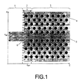
- Figure 1 provides a schematic view of the coupling structure for a specific case based on the introduction of a defect (6) into the coupling structure (2) of length L necessary for achieving the adaptation of the widths between the dielectric guide (1) and the photonic crystal guide (3).
- the adaptation structure (2) is formed by eliminating the appropriate cylinders in order to increase the width of the photonic crystal guide up to a width similar to that of the dielectric guide.
- the photonic crystal consists of a series of cylinders (4) arranged according to two-dimensional triangular periodic grid with grid constant a .
- the radius of the cylinders is R and they consist of a material with a refraction index different to that of the medium (5) that surrounds the columns.
- the coupling technique is valid both for inserting light from a dielectric guide into a photonic crystal guide as for extracting light from a photonic crystal guide into a dielectric guide.
- the specific structure described here comprises a two-dimensional grid of cylinders with a high refraction index on a planar substratum with a lower refraction index
- the coupling technique is equally valid in the case of a structure formed by a two-dimensional grid of air gaps in a substratum with a high refraction index, as the coupling technique's underlying physical principles are the same.
- the input or output dielectric optical guide is made from the same material that comprises the substratum of the photonic crystal.
- the number and arrangement of the defects may be different to that shown in Figure 1.
- the value of the refraction index may also be different in each one of the possible defects.
- An example with an alternative distribution of defects is shown in Figure 2 in a three-dimensional depiction. In this case, we may observe that two defects (7,8) have been introduced in order to maximise coupling.
- the crystal has one dielectric layer a bove (9) and a nother one below (10).
- the refraction index for these two layers must bei dentical for reasons of symmetry and less than the refraction index of the material (5) comprising the waveguides in the crystal. Confinement is thus ensured in the signal's transverse direction when it is propagated along the guide created in the crystal.
- the height of the columns is a design parameter that will depend on the specific characteristics of the photonic crystal.
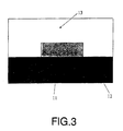
- the cross section of the dielectric guide is shown in Figure 3.
- the dielectric guide consists of a nucleus (11) surrounded by an upper (13) and lower (12) layer.
- the refraction index of the nucleus (11) must be greater than the refraction index of the upper (13) and lower (12) layers to ensure guiding by means of total internal reflection.
- the refraction index for the upper (13) and lower (12) layers may be different provided that the aforementioned condition is fulfilled.
- Figure 4 shows a three-dimensional cross section of the structure depicted in Figure 2.
- the two defects (7,8) with different radii r 1 and r 2 .
- the relative position within the coupling structure is different being ( X def_1 , Z def_1 ) for defect (7) and ( X def_2 , Z def_2 ) for defect (8).
- the number of defects as well as their characteristics will depend both on the size of the adaptation structure L T and on its width W T .
- a possible method for choosing the most appropriate number and position of defects is to perform a sweeping with a single defect on the z-axis maintaining it on the specular axis of symmetry of the guide, with the direction of the axes being as shown in Figure 4.
- the transmission response obtained has an oscillating shape with a series of peaks of different amplitude on the z-axis. Coupling efficiency may then be maximised by suitably fitting the defects into these positions and subsequently obtaining the optimum radius for each one of them.
- Figures 5 and 6 show the results obtained by simulation employing the finite-difference time-domain (FDTD).
- Coupling length L is 0.5 ⁇ m.
- the wavelength considered is 1.55 ⁇ m, a value commonly employed for optical communications.
- the crystal consists of columns with a refraction index of 3.4 that emulates a Silicon (Si) material for the wavelength considered.
- the material that surrounds the columns registers a refraction index of 1.45 corresponding to a Silicon Oxide (SiO 2 ) material for the wavelength considered.
- the columns are arranged in the manner of a triangular grid with a grid constant, a , of 465 nm and a radius of 0.2 a .
- the crystal with these characteristics presents a forbidden band in the standardised range of frequencies between 0.26 a / ⁇ and 0.36 a / ⁇ .
- the input dielectric guide has a refraction index of 1.45.
- the material above and below the guide is air.
- Figure 5 shows the transmission response in terms of the width of the dielectric guide standardised by the grid constant (14-16), the radius of the defect standardised by the radius of the columns that form the crystal (17) and the relative position of the defect on the z-axis standardised by the grid constant (18).
- the input signal is considered to be a flat monochromatic wave whose wavelength is 1.55 ⁇ m. At said wavelength there are guided modes both in the dielectric guide and in the photonic crystal guide.
- the width standardised to the grid constant the coupling structure is shown with defect (14), without defect (15) and for direct coupling without any coupling structure (16). It is observed that the transmission for (14) exceeds the other two cases, exceeding 80% for a wide range of width values for the input dielectric guide. An optimum is achieved for 3.22 a , which corresponds to a width of 1.5 ⁇ m for the grid constant value considered.
- the optimum radius for the defect is obtained on the basis of the graph (17) wherein one may observe the variation of transmission with the radius of the defect considering the width of the optimum dielectric guide obtained previously. It is observed that the transmission peak is given by 0.5 R , which was the value used to find the prior results (14-16).
- the optimum position standardised by the grid constant on the x and z axes has been obtained, with their direction being that shown in Figure 1.
- the optimum position on the x -axis coincides with the structure's specular axis of symmetry, as is observed in the graph (18).
- the optimum position on the z -axis is 0.6 a , taking into account the origin of the coordinates shown in (19). In this case, transmission improves from 84.6% to 87.5% regarding the value of 0.5 a considered previously.
- Figure 6 shows the frequency spectrum for the response in transmission (20, 21) and in reflection in standardised linear units (22, 23) with this latter case solely considering reflection in the dielectric guide.
- the results for the coupling structure with defect correspond to (20) and (22) whilst results (21) and (23) correspond to the coupling structure without defect. It is observed that the introduction of the defect significantly improves transmission (20) with regard to the case without defect (21). Consequently, reflection in the dielectric guide is also much lower for the coupling structure with defect (22) with regard to the structure without defect (23).
- Transmission encompasses the whole range of standardised frequencies for which there exists the mode that appears within the crystal's forbidden band and which is propagated in the photonic crystal guide. Mean transmission within this frequency margin is 78.5%, which is a 30% improvement on the value obtained by means of the coupling structure without defect.
Landscapes
- Engineering & Computer Science (AREA)
- Physics & Mathematics (AREA)
- Optics & Photonics (AREA)
- Chemical & Material Sciences (AREA)
- Nanotechnology (AREA)
- Microelectronics & Electronic Packaging (AREA)
- General Physics & Mathematics (AREA)
- Life Sciences & Earth Sciences (AREA)
- Biophysics (AREA)
- Crystallography & Structural Chemistry (AREA)
- Optical Integrated Circuits (AREA)
- Optical Couplings Of Light Guides (AREA)
Applications Claiming Priority (3)
| Application Number | Priority Date | Filing Date | Title |
|---|---|---|---|
| ES200201931A ES2199693B1 (es) | 2002-08-14 | 2002-08-14 | Sistema de acoplamiento entre guias opticas dielectricas y guias en cristales fotonicos planares. |
| ES200201931 | 2002-08-14 | ||
| PCT/ES2003/000421 WO2004017113A1 (es) | 2002-08-14 | 2003-08-13 | Sistema de acoplamiento entre guías ópticas dieléctricas y guías en cristales fotónicos planares |
Publications (1)
| Publication Number | Publication Date |
|---|---|
| EP1544650A1 true EP1544650A1 (de) | 2005-06-22 |
Family
ID=31725574
Family Applications (1)
| Application Number | Title | Priority Date | Filing Date |
|---|---|---|---|
| EP03787823A Withdrawn EP1544650A1 (de) | 2002-08-14 | 2003-08-13 | Koppelsystem zwischen dielektrischen optischen leitern und planaren photonischen kristalleitern |
Country Status (4)
| Country | Link |
|---|---|
| EP (1) | EP1544650A1 (de) |
| JP (1) | JP2005535926A (de) |
| ES (1) | ES2199693B1 (de) |
| WO (1) | WO2004017113A1 (de) |
Cited By (2)
| Publication number | Priority date | Publication date | Assignee | Title |
|---|---|---|---|---|
| ES2238906A1 (es) * | 2003-07-10 | 2005-09-01 | Universidad Autonoma De Madrid | Convertidor optico. |
| CN103076306A (zh) * | 2012-06-11 | 2013-05-01 | 北京邮电大学 | 一种基于级联硅波导与边腔耦合的光子晶体传感器阵列 |
Families Citing this family (2)
| Publication number | Priority date | Publication date | Assignee | Title |
|---|---|---|---|---|
| DE102009030338B4 (de) | 2009-06-18 | 2018-01-04 | Fraunhofer-Gesellschaft zur Förderung der angewandten Forschung e.V. | Optische Interferenzanordnung und Verfahren zur Einkopplung von elektromagnetischer Strahlung in einen photonischen Kristall oder Quasikristall |
| CN112987294B (zh) * | 2019-12-16 | 2024-09-20 | 杭州光粒科技有限公司 | 一种二维光波导、虚实光波合束器以及ar设备 |
Family Cites Families (5)
| Publication number | Priority date | Publication date | Assignee | Title |
|---|---|---|---|---|
| JP3456166B2 (ja) * | 1999-06-23 | 2003-10-14 | 日本電気株式会社 | フォトニック結晶を用いた光結合素子および光結合方法 |
| DE10123137C1 (de) * | 2001-04-30 | 2002-10-17 | Hertz Inst Heinrich | Integriert-optischer Feldweitentransformator zur adiabatischen, monomodigen Feldanpassung |
| JP3846228B2 (ja) * | 2001-06-07 | 2006-11-15 | 日本電気株式会社 | 導波路 |
| US6782169B2 (en) * | 2001-09-05 | 2004-08-24 | University Of Delaware | System for efficient coupling to photonic crystal waveguides |
| FR2837003B1 (fr) * | 2002-03-05 | 2004-06-04 | Cit Alcatel | Dispositif optique comportant un adaptateur de mode sur composant optique a bande interdite photonique |
-
2002
- 2002-08-14 ES ES200201931A patent/ES2199693B1/es not_active Expired - Fee Related
-
2003
- 2003-08-13 EP EP03787823A patent/EP1544650A1/de not_active Withdrawn
- 2003-08-13 JP JP2004528530A patent/JP2005535926A/ja active Pending
- 2003-08-13 WO PCT/ES2003/000421 patent/WO2004017113A1/es not_active Ceased
Non-Patent Citations (1)
| Title |
|---|
| See references of WO2004017113A1 * |
Cited By (3)
| Publication number | Priority date | Publication date | Assignee | Title |
|---|---|---|---|---|
| ES2238906A1 (es) * | 2003-07-10 | 2005-09-01 | Universidad Autonoma De Madrid | Convertidor optico. |
| ES2238906B1 (es) * | 2003-07-10 | 2006-11-16 | Universidad Autonoma De Madrid | Convertidor optico. |
| CN103076306A (zh) * | 2012-06-11 | 2013-05-01 | 北京邮电大学 | 一种基于级联硅波导与边腔耦合的光子晶体传感器阵列 |
Also Published As
| Publication number | Publication date |
|---|---|
| JP2005535926A (ja) | 2005-11-24 |
| ES2199693A1 (es) | 2004-02-16 |
| WO2004017113A1 (es) | 2004-02-26 |
| ES2199693B1 (es) | 2005-05-01 |
Similar Documents
| Publication | Publication Date | Title |
|---|---|---|
| Chutinan et al. | Waveguides and waveguide bends in two-dimensional photonic crystal slabs | |
| EP1219984B1 (de) | Photonenkristall-Wellenleiter | |
| Engelen et al. | Two regimes of slow-light losses revealed by adiabatic reduction of group velocity | |
| Chutinan et al. | Wider bandwidth with high transmission through waveguide bends in two-dimensional photonic crystal slabs | |
| Astratov et al. | Heavy photon dispersions in photonic crystal waveguides | |
| Miyai et al. | Analysis of coupling between two-dimensional photonic crystal waveguide and external waveguide | |
| Sanchis et al. | High efficiency coupling technique for planar photonic crystal waveguides | |
| El Hassouani et al. | Surface electromagnetic waves in Fibonacci superlattices: Theoretical and experimental results | |
| Böttger et al. | Improved transmission characteristics of moderate refractive index contrast photonic crystal slabs | |
| EP1544650A1 (de) | Koppelsystem zwischen dielektrischen optischen leitern und planaren photonischen kristalleitern | |
| US20060153500A1 (en) | Coupling system between dielectric optical guides and planar photonic crystal guides | |
| Joannopoulos | The almost-magical world of photonic crystals | |
| Foghani et al. | Simulation and design of a wideband T-shaped photonic crystal splitter | |
| Yamada et al. | SOI-based photonic crystal line-defect waveguides | |
| Lin et al. | Sensitivity to termination morphology of light coupling in photonic-crystal waveguides | |
| Lee et al. | Transmission characteristics of various bent periodic dielectric waveguides | |
| Martinez et al. | Wavelength demultiplexing structure based on coupled-cavity waveguides in photonic crystals | |
| Tsarev | Silicon wire waveguide crossing with negligible loss and crosstalk | |
| Furuya et al. | Novel Ring Waveguide Device in a 2D Photonic Crystal Slab–Transmittance Simulated by Finit-Difference Time-Domain Analysis– | |
| Damask | Practical design of side-coupled quarter-wave shifted distributed-Bragg resonant filters | |
| Dekkiche et al. | Improved transmission for photonic crystal Y-junctions | |
| Fakharzadeh et al. | Design and analysis of ultra-miniaturized meandering photonic crystals delay lines | |
| Shinya et al. | Single-mode transmission in commensurate width-varied line-defect SOI photonic crystal waveguides | |
| Joannopoulos | An introduction to photonic crystals | |
| Rubio-Mercedes et al. | Periodic segmented waveguide analysis by using the 2D finite element method |
Legal Events
| Date | Code | Title | Description |
|---|---|---|---|
| PUAI | Public reference made under article 153(3) epc to a published international application that has entered the european phase |
Free format text: ORIGINAL CODE: 0009012 |
|
| 17P | Request for examination filed |
Effective date: 20050215 |
|
| AK | Designated contracting states |
Kind code of ref document: A1 Designated state(s): AT BE BG CH CY CZ DE DK EE ES FI FR GB GR HU IE IT LI LU MC NL PT RO SE SI SK TR |
|
| 17Q | First examination report despatched |
Effective date: 20060929 |
|
| STAA | Information on the status of an ep patent application or granted ep patent |
Free format text: STATUS: THE APPLICATION IS DEEMED TO BE WITHDRAWN |
|
| 18D | Application deemed to be withdrawn |
Effective date: 20090303 |