EP1542292A1 - Light emitting device - Google Patents
Light emitting device Download PDFInfo
- Publication number
- EP1542292A1 EP1542292A1 EP04735500A EP04735500A EP1542292A1 EP 1542292 A1 EP1542292 A1 EP 1542292A1 EP 04735500 A EP04735500 A EP 04735500A EP 04735500 A EP04735500 A EP 04735500A EP 1542292 A1 EP1542292 A1 EP 1542292A1
- Authority
- EP
- European Patent Office
- Prior art keywords
- light emitting
- emitting device
- substrate
- uneven
- semiconductor layer
- Prior art date
- Legal status (The legal status is an assumption and is not a legal conclusion. Google has not performed a legal analysis and makes no representation as to the accuracy of the status listed.)
- Withdrawn
Links
- 239000000758 substrate Substances 0.000 claims abstract description 52
- 239000004065 semiconductor Substances 0.000 claims abstract description 37
- 239000013078 crystal Substances 0.000 description 12
- 230000000052 comparative effect Effects 0.000 description 11
- 238000000034 method Methods 0.000 description 7
- 150000004767 nitrides Chemical class 0.000 description 6
- 238000001228 spectrum Methods 0.000 description 6
- 238000010586 diagram Methods 0.000 description 5
- JMASRVWKEDWRBT-UHFFFAOYSA-N Gallium nitride Chemical compound [Ga]#N JMASRVWKEDWRBT-UHFFFAOYSA-N 0.000 description 3
- 238000002488 metal-organic chemical vapour deposition Methods 0.000 description 3
- 239000000203 mixture Substances 0.000 description 3
- 229910052594 sapphire Inorganic materials 0.000 description 3
- 239000010980 sapphire Substances 0.000 description 3
- 239000003086 colorant Substances 0.000 description 2
- 238000001451 molecular beam epitaxy Methods 0.000 description 2
- 239000000126 substance Substances 0.000 description 2
- 238000000927 vapour-phase epitaxy Methods 0.000 description 2
- 229910002704 AlGaN Inorganic materials 0.000 description 1
- 238000002441 X-ray diffraction Methods 0.000 description 1
- 230000015572 biosynthetic process Effects 0.000 description 1
- 238000005229 chemical vapour deposition Methods 0.000 description 1
- 150000001875 compounds Chemical class 0.000 description 1
- 230000007547 defect Effects 0.000 description 1
- 239000012212 insulator Substances 0.000 description 1
- 238000004519 manufacturing process Methods 0.000 description 1
- 239000002184 metal Substances 0.000 description 1
- 238000012986 modification Methods 0.000 description 1
- 230000004048 modification Effects 0.000 description 1
Images


Classifications
-
- H—ELECTRICITY
- H10—SEMICONDUCTOR DEVICES; ELECTRIC SOLID-STATE DEVICES NOT OTHERWISE PROVIDED FOR
- H10H—INORGANIC LIGHT-EMITTING SEMICONDUCTOR DEVICES HAVING POTENTIAL BARRIERS
- H10H20/00—Individual inorganic light-emitting semiconductor devices having potential barriers, e.g. light-emitting diodes [LED]
- H10H20/80—Constructional details
- H10H20/81—Bodies
- H10H20/819—Bodies characterised by their shape, e.g. curved or truncated substrates
-
- H—ELECTRICITY
- H10—SEMICONDUCTOR DEVICES; ELECTRIC SOLID-STATE DEVICES NOT OTHERWISE PROVIDED FOR
- H10H—INORGANIC LIGHT-EMITTING SEMICONDUCTOR DEVICES HAVING POTENTIAL BARRIERS
- H10H20/00—Individual inorganic light-emitting semiconductor devices having potential barriers, e.g. light-emitting diodes [LED]
- H10H20/80—Constructional details
- H10H20/81—Bodies
- H10H20/819—Bodies characterised by their shape, e.g. curved or truncated substrates
- H10H20/821—Bodies characterised by their shape, e.g. curved or truncated substrates of the light-emitting regions, e.g. non-planar junctions
Definitions
- the present invention relates to a light emitting device that can emit a large amount of light.
- a light emitting device for three primary colors: "blue”, “green” and “red” of visible light can be fabricated by using a group III nitride semiconductor.
- a group III nitride semiconductor crystal grown on the thus-formed amorphous buffer layer has been proposed (for example, Shibata, "Fabrication of LED Based on III-V Nitride and its Applications", Journal of the Japanese Association for Crystal Growth, vol. 29, No. 3, pp. 283 to 287, Sept. 20, 2002).
- the sapphire substrate is an insulator, there has been a problem in a resultant large size light emitting device.
- a group III nitride semiconductor crystal be grown on a substrate by using a substrate of a group III nitride semiconductor such as n-GaN (for example, Nishida, "AlGaN-based Ultraviolet Light Emitting Diodes", Journal of the Japanese Association for Crystal Growth, vol. 29, No. 3, pp. 288 to 295, Sept. 20, 2002).
- n-GaN for example, Nishida, "AlGaN-based Ultraviolet Light Emitting Diodes", Journal of the Japanese Association for Crystal Growth, vol. 29, No. 3, pp. 288 to 295, Sept. 20, 2002.
- an object of the present invention is to provide a light emitting device in which a light emitting amount is increased without changing the size of the light emitting device.
- the light emitting device is characterized in that a semiconductor layer is formed on an uneven surface of an uneven substrate.
- the uneven substrate can comprise Al x Ga y In 1-x-y N (0 ⁇ x, 0 ⁇ y, x+y ⁇ 1); each of the planes forming the uneven surface of the uneven substrate has at least one plane index selected from among (11-2L) and (1-10L) in which L represents an integer of from 1 to 4; and the angle formed between each of the planes forming an uneven upper surface of the uneven substrate and the base plane can be from 35° to 80°.
- a semiconductor layer 30 is formed on an uneven surface 1a of an uneven substrate 1.
- the surface area of the semiconductor layer 30 for light emission can be large and, accordingly, the light emitting amount of the light emitting device becomes large.
- the semiconductor layer 30 is formed on a planar surface 2h of a plane substrate 2.
- the semiconductor layer 30 of the light emitting device according to the present invention is formed on the uneven surface 1a of the uneven substrate 1, a surface area thereof becomes larger than that of the semiconductor layer 30 formed on the planar surface 2h of the plane substrate 2.
- the semiconductor layer 30 has a constant light emitting amount per unit surface area, by allowing the surface area of the semiconductor layer 30 to be large in such a manner as described above, the light emitting amount can be large without changing the size of the light emitting device.
- the surface shape of the uneven surface 1a of the uneven substrate 1 is not particularly limited and, for example, the uneven surface 1a having triangular peak portions and triangular valley portions as shown in Fig. 3 is permissible, or the uneven surface 1a in a polyhedral pyramidal shape where one peak region is delineated by a broken line, shown in Fig. 4, is permissible.
- peak-valley pitch (horizontal distance between a projection portion and an adjacent projection portion) P in the uneven surface 1a of the uneven substrate 1 and peak-valley height (vertical distance between a recess portion and a projection portion) H are not particularly limited.
- pitch P is preferably from 1 ⁇ m to 3000 ⁇ m and height H is preferably from 0.1 ⁇ m to 3000 ⁇ m.
- the peak-valley pitch P is less than 1 ⁇ m or more than 3000 ⁇ m, it becomes difficult to obtain a uniform epitaxial crystal.
- the uneven height H is less than 0.1 ⁇ m, light emitting area becomes small, while, when it is more than 3000 ⁇ m, it becomes difficult to obtain a uniform epitaxial crystal.
- the peak-valley pitch P is more preferably from 1 ⁇ m to 500 ⁇ m and the peak-valley height H is more preferably from 4 ⁇ m to 1500 ⁇ m.
- the uneven substrate and the semiconductor layer each preferably comprise Al x Ga y In 1-x-y N (0 ⁇ x, 0 ⁇ y, x+y ⁇ 1).
- the semiconductor layer By constructing the semiconductor layer from Al x Ga y In 1-x-y N (0 ⁇ x, 0 ⁇ y, x+y ⁇ 1) which is a group III compound, the light emitting device for three primary colors: "blue", "green” and “red” of visible light or “ultraviolet” can be fabricated.
- Al x Ga y In 1-x-y N (0 ⁇ x, 0 ⁇ y, x+y ⁇ 1) here as in the semiconductor layer, a semiconductor layer of good quality can be grown.
- the chemical composition of the substrate, that of the semiconductor crystal and a combination of these compositions are not particularly limited and, from the standpoint of obtaining semiconductor layer of good quality, the chemical composition of the substrate and that of the semiconductor layer are favorably similar.
- each of planes 1b and 1c forming the uneven surface of the uneven substrate has at least one plane index selected from among (11-2L) and (1-10L) in which L represents an integer of from 1 to 4.
- L represents an integer of from 1 to 4.
- the uneven substrate 1 having the uneven surface 1a comprising such planes as described above, a semiconductor layer of a three-dimensional structure can be formed and, accordingly, the surface area of the semiconductor layer can be large.
- the uneven substrate comprises Al x Ga y In 1-x-y N (0 ⁇ x, 0 ⁇ y, x+y ⁇ 1)
- a hexagonal pyramid or a triangular pyramid is often the polygonal pyramid formed on the uneven surface 1a as shown in Fig. 4.
- angles ⁇ 11b and 11c formed between each of the planes 1b and 1c forming the uneven surface 1a of the uneven substrate 1 and a base plane 1h are preferably from 35° to 80°, respectively.
- the base plane 1h denotes a plane perpendicular to a vector in a thickness direction of the uneven substrate 1 and is a plane parallel to a planar surface in a conventional plane substrate.
- the Al x Ga y In 1-x-y N (0 ⁇ x, 0 ⁇ y, x+y ⁇ 1) crystal constituting the substrate has a wurtzite-type (hexagonal) crystalline structure and, accordingly, has hexagonal symmetry.
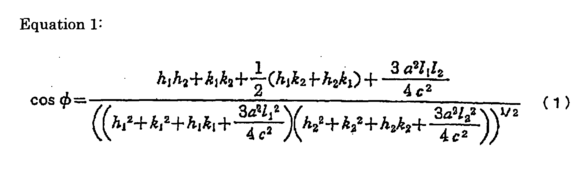
- Each angle ⁇ formed between each of the planes forming the uneven surface and the angle base plane can be computed by Equation (1) as described below.
- (h 1 k 1 -(h 1 +k 1 )l 1 ) denotes a plane index of each of the planes forming the uneven surface
- (h 2 k 2 -(h 2 +k 2 )l 2 ) denotes a plane index of a base plane (for example, (0001))
- a denotes a axis length
- b denotes b axis length
- c denotes c axis length.
- the plane index of each of the planes forming the uneven surface of the uneven substrate and the base plane can be obtained by an X-ray diffraction (hereinafter, referred to as "XRD") method.
- XRD X-ray diffraction
- an n-GaN layer 31 of 5 ⁇ m, an In 0.2 Ga 0.8 N layer 32 of 3 nm, a p-Al 0.2 Ga 0.8 N layer 33 of 60 nm and a p-GaN layer 34 of 150 nm were grown on the uneven surface of the aforementioned GaN substrate in this order by a Metal Organic Chemical Vapor Deposition (hereinafter, referred to as "MOCVD") method, to thereby obtain a light emitting device as shown in Fig.
- MOCVD Metal Organic Chemical Vapor Deposition
- Example 1 A light emitting intensity of the aforementioned light emitting device was measured by using a spectrograph. It has been found that the peak wavelength of a light emitting spectrum of this light emitting device was 470 nm and the light emitting intensity of this light emitting device was 1.9 where the light emitting intensity of Comparative Example 1 to be described below was defined as 1.0. Further, in Example 1, the semiconductor layer was grown on the uneven surface of the uneven substrate by using the MOCVD method. The semiconductor layer can also be grown by using various types of other methods such as Vapor Phase Epitaxy (hereinafter, referred to as "VPE”) method and Molecular Beam Epitaxy (hereinafter, referred to as "MBE”) method.
- VPE Vapor Phase Epitaxy
- MBE Molecular Beam Epitaxy
- a peak wavelength of a light emitting spectrum of this light emitting device was 470 nm, and then, the light emitting intensity of a blue light emitting device of each of the Examples 1 to 9 was compared with the light emitting intensity of this light emitting device defined as 1.0.
- a light emitting device having a substrate and a semiconductor layer constitution as shown in Tables I to III was fabricated by using MOCVD method, and then, the wavelength of a light emitting spectrum and light emitting intensity thereof were measured. The results are collectively shown in Tables I to III. Further, an angle ⁇ in each of the Tables I to III shows the angle as calculated by Eq. 1 from the plane index of each of the planes forming an uneven surface of an uneven substrate and the plane index (0001) of a base plane.
- Examples 1 to 9 and Comparative Example 1 in Table I are each an example of a blue light emitting device in which a peak wavelength of a light emitting spectrum is 470 nm and a light emitting intensity of each of the Examples 1 to 9 was indicated as a relative value where the light emitting intensity of Comparative Example 1 was defined as 1.0.
- Example 10 and Comparative Example 2 in Table II are each an example of a green light emitting device in which the peak wavelength of a light emitting spectrum is 520 nm, and a light emitting intensity of Example 10 was indicated as a relative value where the light emitting intensity of Comparative Example 2 was defined as 1.0; and
- Example 11 and Comparative Example 3 in Table III are each an example of an ultraviolet light emitting device in which a peak wavelength of a light emitting spectrum is 380 nm, and a light emitting intensity of Example 11 was indicated as a relative value where the light emitting intensity of Comparative Example 3 was defined as 1.0.
- Comparative Example 2 Example 10 Type of substrate GaN GaN Shape of substrate Fig. 5 Fig.
- the light emitting intensity has been increased from 1.2 time to 2.5 times, regardless of the light emitting peak wavelength, compared with the conventional light emitting device in which the semiconductor layer was formed on the plane substrate.
- the light emitting amount can be increased by forming a semiconductor layer on an uneven surface of an uneven substrate, without changing the size of the light emitting device.
Landscapes
- Led Devices (AREA)
Abstract
A light emitting device which has increased light emitting amount without changing its size is provided. The light emitting device is characterized in that a semiconductor layer 30 is formed on an uneven surface 1a of an uneven substrate 1. The light emitting device of the invention can be configured such that the uneven substrate and the semiconductor layer are both made of AlxGayIn1-x-yN (0≤x, 0≤y, x+y≤1); each of the planes forming the uneven surface of the uneven substrate has at least one plane index selected from among (11-2L) and (1-10L) in which L represents an integer from 1 to 4; and the angle formed between each of the planes forming the uneven surface of the uneven substrate and the base plane is from 35 DEG to 80 DEG . <IMAGE>
Description
The present invention relates to a light emitting device that can emit a
large amount of light.
A light emitting device for three primary colors: "blue", "green" and
"red" of visible light can be fabricated by using a group III nitride
semiconductor. For example, the formation of an amorphous buffer layer on a
sapphire substrate at low temperature, and then, a group III nitride
semiconductor crystal grown on the thus-formed amorphous buffer layer has
been proposed (for example, Shibata, "Fabrication of LED Based on III-V
Nitride and its Applications", Journal of the Japanese Association for Crystal
Growth, vol. 29, No. 3, pp. 283 to 287, Sept. 20, 2002).
However, since it uses the sapphire substrate as a substrate, even when
a group III nitride semiconductor crystal is epitaxially grown, only crystals of
low quality having a large defect density can be obtained. Further, since the
sapphire substrate is an insulator, there has been a problem in a resultant
large size light emitting device.
In order to solve the aforementioned problem, it has been proposed that
a group III nitride semiconductor crystal be grown on a substrate by using a
substrate of a group III nitride semiconductor such as n-GaN (for example,
Nishida, "AlGaN-based Ultraviolet Light Emitting Diodes", Journal of the
Japanese Association for Crystal Growth, vol. 29, No. 3, pp. 288 to 295, Sept. 20,
2002).
At present, a sufficient light emitting intensity can not be obtained
even by using the aforementioned light emitting device. Under these
circumstances, an object of the present invention is to provide a light emitting
device in which a light emitting amount is increased without changing the size
of the light emitting device.
In order to attain the aforementioned object, the light emitting device
according to the present invention is characterized in that a semiconductor
layer is formed on an uneven surface of an uneven substrate. On this occasion,
the uneven substrate can comprise AlxGayIn1-x-yN (0≤x, 0≤y, x+y≤1); each of the
planes forming the uneven surface of the uneven substrate has at least one
plane index selected from among (11-2L) and (1-10L) in which L represents an
integer of from 1 to 4; and the angle formed between each of the planes forming
an uneven upper surface of the uneven substrate and the base plane can be
from 35° to 80°.
In one light emitting device according to the present invention, in
referring to Fig. 1, a semiconductor layer 30 is formed on an uneven surface 1a
of an uneven substrate 1. By using such uneven substrate 1 as described
above, the surface area of the semiconductor layer 30 for light emission can be
large and, accordingly, the light emitting amount of the light emitting device
becomes large.
On the other hand, in a conventional light emitting device, in reference
to Fig. 2, the semiconductor layer 30 is formed on a planar surface 2h of a plane
substrate 2. Namely, in reference to Figs. 1 and 2, since the semiconductor
layer 30 of the light emitting device according to the present invention is
formed on the uneven surface 1a of the uneven substrate 1, a surface area
thereof becomes larger than that of the semiconductor layer 30 formed on the
planar surface 2h of the plane substrate 2. In this case, since the
semiconductor layer 30 has a constant light emitting amount per unit surface
area, by allowing the surface area of the semiconductor layer 30 to be large in
such a manner as described above, the light emitting amount can be large
without changing the size of the light emitting device.
On this occasion, in reference to Figs. 3 and 4, the surface shape of the
uneven surface 1a of the uneven substrate 1 is not particularly limited and, for
example, the uneven surface 1a having triangular peak portions and triangular
valley portions as shown in Fig. 3 is permissible, or the uneven surface 1a in a
polyhedral pyramidal shape where one peak region is delineated by a broken
line, shown in Fig. 4, is permissible.
Further, peak-valley pitch (horizontal distance between a projection
portion and an adjacent projection portion) P in the uneven surface 1a of the
uneven substrate 1 and peak-valley height (vertical distance between a recess
portion and a projection portion) H are not particularly limited. However, pitch
P is preferably from 1 µm to 3000 µm and height H is preferably from 0.1 µm to
3000 µm. When the peak-valley pitch P is less than 1 µm or more than 3000
µm, it becomes difficult to obtain a uniform epitaxial crystal. When the
uneven height H is less than 0.1 µm, light emitting area becomes small, while,
when it is more than 3000 µm, it becomes difficult to obtain a uniform epitaxial
crystal. Under these circumstances, the peak-valley pitch P is more
preferably from 1 µm to 500 µm and the peak-valley height H is more
preferably from 4 µm to 1500 µm.
In the light emitting device according to the present invention, the
uneven substrate and the semiconductor layer each preferably comprise
AlxGayIn1-x-yN (0≤x, 0≤y, x+y≤1). By constructing the semiconductor layer
from AlxGayIn1-x-yN (0≤x, 0≤y, x+y≤1) which is a group III compound, the light
emitting device for three primary colors: "blue", "green" and "red" of visible
light or "ultraviolet" can be fabricated. Further, also in regards to the
substrate, by using AlxGayIn1-x-yN (0≤x, 0≤y, x+y≤1) here as in the
semiconductor layer, a semiconductor layer of good quality can be grown. Still
further, the chemical composition of the substrate, that of the semiconductor
crystal and a combination of these compositions are not particularly limited
and, from the standpoint of obtaining semiconductor layer of good quality, the
chemical composition of the substrate and that of the semiconductor layer are
favorably similar.
Further, in reference to Figs. 3 and 4, in the light emitting device
according to the present invention, it is preferable that each of planes 1b and 1c
forming the uneven surface of the uneven substrate has at least one plane
index selected from among (11-2L) and (1-10L) in which L represents an integer
of from 1 to 4. In the case in which AlxGayIn1-x-yN (0≤x, 0≤y, x+y≤1) is used in
the substrate and the semiconductor layer, since an AlxGayIn1-x-yN (0≤x, 0≤y,
x+y≤1) crystal has hexagonal symmetry, there exist six equivalent planes with
the same index (11-2L) or (1-10L). On this occasion, L denotes an integer from
1 to 4. Therefore, by using the uneven substrate 1 having the uneven surface
1a comprising such planes as described above, a semiconductor layer of a
three-dimensional structure can be formed and, accordingly, the surface area of
the semiconductor layer can be large. On this occasion, in the case in which
the uneven substrate comprises AlxGayIn1-x-yN (0≤x, 0≤y, x+y≤1), a hexagonal
pyramid or a triangular pyramid is often the polygonal pyramid formed on the
uneven surface 1a as shown in Fig. 4.
Further, in reference to Figs. 3 and 4, in the light emitting device
according to the present invention, angles 11b and 11c formed between each
of the planes 1b and 1c forming the uneven surface 1a of the uneven substrate 1
and a base plane 1h are preferably from 35° to 80°, respectively. In the case in
which the AlxGayIn1-x-yN crystal is used as the uneven substrate, a stable peak
having an angle of over 80° seldom exists. Further, when the aforementioned
angle is less than 35°, the surface area of the semiconductor layer is scarcely
increased at all. Here, the base plane 1h denotes a plane perpendicular to a
vector in a thickness direction of the uneven substrate 1 and is a plane parallel
to a planar surface in a conventional plane substrate.
The AlxGayIn1-x-yN (0≤x, 0≤y, x+y≤1) crystal constituting the substrate
has a wurtzite-type (hexagonal) crystalline structure and, accordingly, has
hexagonal symmetry. Each angle formed between each of the planes forming
the uneven surface and the angle base plane can be computed by Equation (1)
as described below. On this occasion, (h1k1-(h1+k1)l1) denotes a plane index of
each of the planes forming the uneven surface; (h2k2-(h2+k2)l2) denotes a plane
index of a base plane (for example, (0001)); a denotes a axis length; b denotes b
axis length; and c denotes c axis length. Further, the plane index of each of
the planes forming the uneven surface of the uneven substrate and the base
plane can be obtained by an X-ray diffraction (hereinafter, referred to as
"XRD") method.
Hereinafter, a light emitting device according to the present invention
will be described in detail with reference to the embodiments.
By using a GaN substrate which had an uneven surface 1a having a
peak-valley pitch P of 200 µm and a peak-valley height H of 190 µm, as shown
in Fig. 3, and in which the plane index of each of the planes 1b forming the
aforementioned uneven surface 1a was (1-101), an n-GaN layer 31 of 5 µm, an
In0.2Ga0.8N layer 32 of 3 nm, a p-Al0.2Ga0.8N layer 33 of 60 nm and a p-GaN
layer 34 of 150 nm were grown on the uneven surface of the aforementioned
GaN substrate in this order by a Metal Organic Chemical Vapor Deposition
(hereinafter, referred to as "MOCVD") method, to thereby obtain a light
emitting device as shown in Fig. 1. A light emitting intensity of the
aforementioned light emitting device was measured by using a spectrograph.
It has been found that the peak wavelength of a light emitting spectrum of this
light emitting device was 470 nm and the light emitting intensity of this light
emitting device was 1.9 where the light emitting intensity of Comparative
Example 1 to be described below was defined as 1.0. Further, in Example 1,
the semiconductor layer was grown on the uneven surface of the uneven
substrate by using the MOCVD method. The semiconductor layer can also be
grown by using various types of other methods such as Vapor Phase Epitaxy
(hereinafter, referred to as "VPE") method and Molecular Beam Epitaxy
(hereinafter, referred to as "MBE") method.
By using a GaN substrate which has a planar surface 2h (since being
planar, peak-valley pitch P is 0 µm and peak-valley height H is 0 µm) as shown
in Fig. 5 and in which a plane index of the aforementioned planar surface 2h
was (0001), semiconductor layers were grown in the same manner as in
Example 1, to thereby obtain a light emitting device as shown in Fig. 2. A
light emitting intensity of the aforementioned light emitting device was
measured by using a spectrograph. A peak wavelength of a light emitting
spectrum of this light emitting device was 470 nm, and then, the light emitting
intensity of a blue light emitting device of each of the Examples 1 to 9 was
compared with the light emitting intensity of this light emitting device defined
as 1.0.
A light emitting device having a substrate and a semiconductor layer
constitution as shown in Tables I to III was fabricated by using MOCVD
method, and then, the wavelength of a light emitting spectrum and light
emitting intensity thereof were measured. The results are collectively shown
in Tables I to III. Further, an angle in each of the Tables I to III shows the
angle as calculated by Eq. 1 from the plane index of each of the planes forming
an uneven surface of an uneven substrate and the plane index (0001) of a base
plane.
On this occasion, Examples 1 to 9 and Comparative Example 1 in Table
I are each an example of a blue light emitting device in which a peak
wavelength of a light emitting spectrum is 470 nm and a light emitting
intensity of each of the Examples 1 to 9 was indicated as a relative value where
the light emitting intensity of Comparative Example 1 was defined as 1.0.
Further, Example 10 and Comparative Example 2 in Table II are each an
example of a green light emitting device in which the peak wavelength of a
light emitting spectrum is 520 nm, and a light emitting intensity of Example 10
was indicated as a relative value where the light emitting intensity of
Comparative Example 2 was defined as 1.0; and Example 11 and Comparative
Example 3 in Table III are each an example of an ultraviolet light emitting
device in which a peak wavelength of a light emitting spectrum is 380 nm, and
a light emitting intensity of Example 11 was indicated as a relative value where
the light emitting intensity of Comparative Example 3 was defined as 1.0.

| Comparative Example 2 | Example 10 | |
| Type of substrate | GaN | GaN |
| Shape of substrate | Fig. 5 | Fig. 3 |
| P (µm) | 0 | 100 |
| H (µm) | 0 | 94 |
| Plane index | (0001) | (1-101) |
| Angle (°) | 0 | 62 |
| Semiconductor layer (thickness nm) | n-GaN(5000)/In0.45Ga0.55N(3)/p-Al0.2Ga0.8N(60)/p-GaN(150) | n-GaN(5000)/In0.45Ga0.55N(3)/p-Al0.2Ga0.8N(60)/p-GaN(150) |
| Light emitting peak wavelength (nm) | 520 | 520 |
| Light emitting intensity ratio | 1.0 | 2.1 |
| Comparative Example 3 | Example 11 | |
| Type of substrate | GaN | GaN |
| Shape of substrate P (µm) H (µm) | Fig. 5 0 0 | Fig. 3 50 47 |
| Plane index | (0001) | (1-101) |
| Angle (°) | 0 | 62 |
| Semiconductor layer (thickness nm) | n-GaN(5000)/ n-Al0.2Ga0.8N (60)/In0.02Ga0.98 N(3)/p-Al0.2Ga0.8 N(60)/p-GaN (150) | n-GaN(5000)/n-Al0.2Ga0.8N (60)/In0.02Ga0.98 N(3)/p-Al0.2Ga 0.8N(60)/p-GaN(150) |
| Light emitting peak wavelength (nm) | 380 | 380 |
| Light emitting intensity ratio | 1.0 | 1.8 |
As shown in Tables I to III, in the light emitting device, in which the
semiconductor layer was formed on the uneven surface of the uneven substrate,
according to the present invention, the light emitting intensity has been
increased from 1.2 time to 2.5 times, regardless of the light emitting peak
wavelength, compared with the conventional light emitting device in which the
semiconductor layer was formed on the plane substrate.
It is to be understood that embodiments and examples disclosed herein
are illustrative and not restrictive in all aspects. The scope of the invention
should be determined with reference to the appended claims and not to the
above descriptions and is intended to include meanings equivalent to such
claims and all such modifications and variations as fall within the scope of such
claims.
As has been described above, in a light emitting device according to the
present invention, the light emitting amount can be increased by forming a
semiconductor layer on an uneven surface of an uneven substrate, without
changing the size of the light emitting device.
Claims (4)
- A light emitting device, being characterized by forming a semiconductor layer on an uneven surface of an uneven substrate.
- The light emitting device as set forth in Claim 1, wherein the uneven substrate and the semiconductor layer comprise AlxGayIn1-x-yN (0≤x, 0≤y, x+y≤1).
- The light emitting device as set forth in Claim 1 or 2, wherein each of the planes forming the uneven surface of the uneven substrate has at least one plane index selected from among (11-2L) and (1-10L), wherein L represents an integer from 1 to 4.
- The light emitting device as set forth in Claim 1 or 2, wherein the angle formed between each of the planes forming the uneven surface of the uneven substrate and the base plane is from 35° to 80°.
Applications Claiming Priority (3)
| Application Number | Priority Date | Filing Date | Title |
|---|---|---|---|
| JP2003173465A JP2005011944A (en) | 2003-06-18 | 2003-06-18 | Light emitting device |
| JP2003173465 | 2003-06-18 | ||
| PCT/JP2004/007873 WO2004114420A1 (en) | 2003-06-18 | 2004-05-31 | Light emitting device |
Publications (1)
| Publication Number | Publication Date |
|---|---|
| EP1542292A1 true EP1542292A1 (en) | 2005-06-15 |
Family
ID=33534724
Family Applications (1)
| Application Number | Title | Priority Date | Filing Date |
|---|---|---|---|
| EP04735500A Withdrawn EP1542292A1 (en) | 2003-06-18 | 2004-05-31 | Light emitting device |
Country Status (6)
| Country | Link |
|---|---|
| US (1) | US20060054942A1 (en) |
| EP (1) | EP1542292A1 (en) |
| JP (1) | JP2005011944A (en) |
| CN (1) | CN1701447A (en) |
| TW (1) | TW200511609A (en) |
| WO (1) | WO2004114420A1 (en) |
Cited By (1)
| Publication number | Priority date | Publication date | Assignee | Title |
|---|---|---|---|---|
| DE102006043400A1 (en) * | 2006-09-15 | 2008-03-27 | Osram Opto Semiconductors Gmbh | Optoelectronic semiconductor chip |
Families Citing this family (13)
| Publication number | Priority date | Publication date | Assignee | Title |
|---|---|---|---|---|
| KR100649641B1 (en) * | 2005-05-31 | 2006-11-27 | 삼성전기주식회사 | LED Package |
| KR100682877B1 (en) | 2005-07-12 | 2007-02-15 | 삼성전기주식회사 | Light emitting diode and manufacturing method |
| KR100649769B1 (en) | 2005-12-28 | 2006-11-27 | 삼성전기주식회사 | Semiconductor Light Emitting Diode and Manufacturing Method Thereof |
| JP5165264B2 (en) | 2007-03-22 | 2013-03-21 | 浜松ホトニクス株式会社 | Nitride semiconductor substrate |
| CN101661981B (en) * | 2008-08-29 | 2014-10-22 | 广镓光电股份有限公司 | Base plate for making luminous element and luminous element made by same |
| JP5229270B2 (en) * | 2010-05-14 | 2013-07-03 | 豊田合成株式会社 | Group III nitride semiconductor light emitting device manufacturing method |
| TWI540756B (en) | 2010-08-06 | 2016-07-01 | 日亞化學工業股份有限公司 | Sapphire substrate and semiconductor light emitting device |
| JP5980667B2 (en) * | 2011-12-03 | 2016-08-31 | ツィンファ ユニバーシティ | Light emitting diode |
| JP5980668B2 (en) * | 2011-12-03 | 2016-08-31 | ツィンファ ユニバーシティ | Light emitting diode |
| JP5980669B2 (en) * | 2011-12-03 | 2016-08-31 | ツィンファ ユニバーシティ | Light emitting diode |
| JP2013140879A (en) * | 2012-01-05 | 2013-07-18 | Ushio Inc | Electron beam pumped light source device |
| CN102867896B (en) * | 2012-09-26 | 2015-10-14 | 湘能华磊光电股份有限公司 | LED epitaxial structure and preparation method thereof |
| JP6755230B2 (en) * | 2017-11-16 | 2020-09-16 | シャープ株式会社 | Nitride semiconductor light emitting device and method for manufacturing nitride semiconductor light emitting device |
Family Cites Families (5)
| Publication number | Priority date | Publication date | Assignee | Title |
|---|---|---|---|---|
| JPH0715033A (en) * | 1993-06-28 | 1995-01-17 | Japan Energy Corp | Semiconductor light emitting device |
| JP3240097B2 (en) * | 1995-02-16 | 2001-12-17 | シャープ株式会社 | Semiconductor light emitting device |
| JP2003092426A (en) * | 2001-09-18 | 2003-03-28 | Nichia Chem Ind Ltd | Nitride compound semiconductor light emitting device and method of manufacturing the same |
| US7042150B2 (en) * | 2002-12-20 | 2006-05-09 | Showa Denko K.K. | Light-emitting device, method of fabricating the device, and LED lamp using the device |
| KR100504180B1 (en) * | 2003-01-29 | 2005-07-28 | 엘지전자 주식회사 | crystal growth method of nitride compound semiconductor |
-
2003
- 2003-06-18 JP JP2003173465A patent/JP2005011944A/en not_active Withdrawn
-
2004
- 2004-05-31 CN CN200480000800.8A patent/CN1701447A/en active Pending
- 2004-05-31 EP EP04735500A patent/EP1542292A1/en not_active Withdrawn
- 2004-05-31 US US10/522,829 patent/US20060054942A1/en not_active Abandoned
- 2004-05-31 WO PCT/JP2004/007873 patent/WO2004114420A1/en not_active Ceased
- 2004-06-02 TW TW093115831A patent/TW200511609A/en unknown
Non-Patent Citations (1)
| Title |
|---|
| See references of WO2004114420A1 * |
Cited By (2)
| Publication number | Priority date | Publication date | Assignee | Title |
|---|---|---|---|---|
| DE102006043400A1 (en) * | 2006-09-15 | 2008-03-27 | Osram Opto Semiconductors Gmbh | Optoelectronic semiconductor chip |
| EP1901357A3 (en) * | 2006-09-15 | 2013-07-31 | OSRAM Opto Semiconductors GmbH | Optoelectronic semiconductor chip |
Also Published As
| Publication number | Publication date |
|---|---|
| JP2005011944A (en) | 2005-01-13 |
| WO2004114420A1 (en) | 2004-12-29 |
| CN1701447A (en) | 2005-11-23 |
| US20060054942A1 (en) | 2006-03-16 |
| TW200511609A (en) | 2005-03-16 |
Similar Documents
| Publication | Publication Date | Title |
|---|---|---|
| JP4432180B2 (en) | Group III nitride compound semiconductor manufacturing method, group III nitride compound semiconductor device, and group III nitride compound semiconductor | |
| JP3556916B2 (en) | Manufacturing method of semiconductor substrate | |
| JP3471685B2 (en) | Semiconductor substrate and manufacturing method thereof | |
| US6830948B2 (en) | Method for producing group III nitride compound semiconductor and group III nitride compound semiconductor device | |
| JP3763753B2 (en) | Group III nitride compound semiconductor device and method for manufacturing the same | |
| EP1278233A1 (en) | Production method of iii nitride compound semiconductor substrate and semiconductor device | |
| KR20010031642A (en) | GaN SINGLE CRYSTALLINE SUBSTRATE AND METHOD OF PRODUCING THE SAME | |
| TWI416612B (en) | Semiconductor component and method of manufacturing same | |
| JPH11251253A (en) | Method for manufacturing nitride semiconductor substrate and nitride semiconductor substrate | |
| JP2004288799A (en) | Semiconductor light emitting element and its manufacturing method, integrated semiconductor light emitting device and its manufacturing method, image display device and its manufacturing method, and lighting device and its manufacturing method | |
| JP2001267242A (en) | Group III nitride compound semiconductor and method of manufacturing the same | |
| WO2010016532A1 (en) | Group iii nitride semiconductor laminate structure and method for manufacturing the group iii nitride semiconductor laminate structure | |
| US20060054942A1 (en) | Light emitting device | |
| US6844246B2 (en) | Production method of III nitride compound semiconductor, and III nitride compound semiconductor element based on it | |
| TWI520325B (en) | Manufacture of nitride semiconductor structures | |
| JP4406999B2 (en) | Group III nitride compound semiconductor manufacturing method and group III nitride compound semiconductor device | |
| JP4051892B2 (en) | Group III nitride compound semiconductor manufacturing method and group III nitride compound semiconductor device | |
| JP4698053B2 (en) | Method for producing group III nitride compound semiconductor | |
| JP3680751B2 (en) | Group III nitride compound semiconductor manufacturing method and group III nitride compound semiconductor device | |
| JP2003124576A (en) | Nitride semiconductor substrate and growth method thereof | |
| US12155006B2 (en) | Light-emitting diode and manufacturing method | |
| JP7305428B2 (en) | Semiconductor growth substrate, semiconductor device, semiconductor light-emitting device, and semiconductor device manufacturing method | |
| JP4985579B2 (en) | Group III nitride compound semiconductor and gallium nitride free-standing substrate manufacturing method | |
| JP4016566B2 (en) | Group III nitride compound semiconductor manufacturing method and group III nitride compound semiconductor device | |
| JP2007317752A (en) | Template board |
Legal Events
| Date | Code | Title | Description |
|---|---|---|---|
| PUAI | Public reference made under article 153(3) epc to a published international application that has entered the european phase |
Free format text: ORIGINAL CODE: 0009012 |
|
| 17P | Request for examination filed |
Effective date: 20050118 |
|
| AK | Designated contracting states |
Kind code of ref document: A1 Designated state(s): AT BE BG CH CY CZ DE DK EE ES FI FR GB GR HU IE IT LI LU MC NL PL PT RO SE SI SK TR |
|
| AX | Request for extension of the european patent |
Extension state: AL HR LT LV MK |
|
| STAA | Information on the status of an ep patent application or granted ep patent |
Free format text: STATUS: THE APPLICATION HAS BEEN WITHDRAWN |
|
| 18W | Application withdrawn |
Effective date: 20051103 |