EP1542283A2 - Method for fabricating organic electr-luminance device - Google Patents
Method for fabricating organic electr-luminance device Download PDFInfo
- Publication number
- EP1542283A2 EP1542283A2 EP04029332A EP04029332A EP1542283A2 EP 1542283 A2 EP1542283 A2 EP 1542283A2 EP 04029332 A EP04029332 A EP 04029332A EP 04029332 A EP04029332 A EP 04029332A EP 1542283 A2 EP1542283 A2 EP 1542283A2
- Authority
- EP
- European Patent Office
- Prior art keywords
- electrode
- insulating layer
- forming
- electrode separator
- organic
- Prior art date
- Legal status (The legal status is an assumption and is not a legal conclusion. Google has not performed a legal analysis and makes no representation as to the accuracy of the status listed.)
- Granted
Links
Images






Classifications
-
- H—ELECTRICITY
- H10—SEMICONDUCTOR DEVICES; ELECTRIC SOLID-STATE DEVICES NOT OTHERWISE PROVIDED FOR
- H10K—ORGANIC ELECTRIC SOLID-STATE DEVICES
- H10K59/00—Integrated devices, or assemblies of multiple devices, comprising at least one organic light-emitting element covered by group H10K50/00
- H10K59/10—OLED displays
- H10K59/12—Active-matrix OLED [AMOLED] displays
- H10K59/122—Pixel-defining structures or layers, e.g. banks
-
- H—ELECTRICITY
- H05—ELECTRIC TECHNIQUES NOT OTHERWISE PROVIDED FOR
- H05B—ELECTRIC HEATING; ELECTRIC LIGHT SOURCES NOT OTHERWISE PROVIDED FOR; CIRCUIT ARRANGEMENTS FOR ELECTRIC LIGHT SOURCES, IN GENERAL
- H05B33/00—Electroluminescent light sources
- H05B33/10—Apparatus or processes specially adapted to the manufacture of electroluminescent light sources
-
- H—ELECTRICITY
- H10—SEMICONDUCTOR DEVICES; ELECTRIC SOLID-STATE DEVICES NOT OTHERWISE PROVIDED FOR
- H10K—ORGANIC ELECTRIC SOLID-STATE DEVICES
- H10K50/00—Organic light-emitting devices
- H10K50/80—Constructional details
- H10K50/805—Electrodes
- H10K50/81—Anodes
- H10K50/818—Reflective anodes, e.g. ITO combined with thick metallic layers
-
- H—ELECTRICITY
- H10—SEMICONDUCTOR DEVICES; ELECTRIC SOLID-STATE DEVICES NOT OTHERWISE PROVIDED FOR
- H10K—ORGANIC ELECTRIC SOLID-STATE DEVICES
- H10K59/00—Integrated devices, or assemblies of multiple devices, comprising at least one organic light-emitting element covered by group H10K50/00
- H10K59/80—Constructional details
- H10K59/805—Electrodes
- H10K59/8051—Anodes
- H10K59/80518—Reflective anodes, e.g. ITO combined with thick metallic layers
-
- H—ELECTRICITY
- H10—SEMICONDUCTOR DEVICES; ELECTRIC SOLID-STATE DEVICES NOT OTHERWISE PROVIDED FOR
- H10K—ORGANIC ELECTRIC SOLID-STATE DEVICES
- H10K2102/00—Constructional details relating to the organic devices covered by this subclass
- H10K2102/301—Details of OLEDs
- H10K2102/302—Details of OLEDs of OLED structures
- H10K2102/3023—Direction of light emission
- H10K2102/3026—Top emission
-
- Y—GENERAL TAGGING OF NEW TECHNOLOGICAL DEVELOPMENTS; GENERAL TAGGING OF CROSS-SECTIONAL TECHNOLOGIES SPANNING OVER SEVERAL SECTIONS OF THE IPC; TECHNICAL SUBJECTS COVERED BY FORMER USPC CROSS-REFERENCE ART COLLECTIONS [XRACs] AND DIGESTS
- Y10—TECHNICAL SUBJECTS COVERED BY FORMER USPC
- Y10S—TECHNICAL SUBJECTS COVERED BY FORMER USPC CROSS-REFERENCE ART COLLECTIONS [XRACs] AND DIGESTS
- Y10S428/00—Stock material or miscellaneous articles
- Y10S428/917—Electroluminescent
Definitions
- the present invention relates to a flat panel display, and more particularly, to a method for fabricating an organic EL device that can prevent delamination of an electrode.
- the organic EL device is a device to emit light while an electron and a hole are injected into an organic emission layer disposed between a first electrode, electron injection electrode (cathode) and a second electrode, hole injection electrode (anode), the electron and the hole are bonded to form a pair of electron and hole and generate an exciton, and the generated exciton disappears from an excited state to a base state.
- Such an organic EL device is being actively researched due to a relatively low operation voltage of 5 - 10 V compared with a plasma display panel (PDP) or an inorganic EL display.
- PDP plasma display panel
- inorganic EL display Such an organic EL device is being actively researched due to a relatively low operation voltage of 5 - 10 V compared with a plasma display panel (PDP) or an inorganic EL display.
- the organic EL device has superior features such as a wide viewing angle, a high speed response and a high contrast.
- the organic EL device can be used as a pixel of a graphic display, a television image display or a pixel of a surface light source.
- the organic EL device can be formed on a flexible transparent substrate and has slim, lightweight and good color sense characteristics, it is suitable for a next generation flat panel display (FDP).
- FDP next generation flat panel display
- the organic EL device does not need a backlight compared with the LCD well known, it has advantages such as a low power consumption and a superior color sense.
- the organic EL devices can be classified into a passive matrix type and an active matrix type.
- the active matrix type organic EL device when light is emitted through the glass surface, which is generally called ⁇ bottom emission' , as the size or the number of thin film transistors (TFT) increases, the aperture ratio is reduced by geometric progression, which makes it impossible to use the active matrix type organic EL device as a display device.
- TFT thin film transistors
- the top emission organic El device includes a substrate having TFTs and storage capacitors formed thereon, a reflective layer formed on the substrate, and an organic emission layer and a transparent electrode layer sequentially formed on the reflective layer. Light emitted from the organic emission layer is reflected by the reflective layer and then emitted toward an opposite direction to the substrate. Accordingly, the aperture ratio is not lowered due to the TFTs.
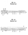
- FIGs. 1A through 1F Next, a method for fabricating a top emission active type organic EL device according to the related art will be described with reference to FIGs. 1A through 1F.
- a thin film transistor (TFT) 12 is formed in the unit of pixel on a transparent substrate 11.
- amorphous silicon is formed on the transparent substrate 11.
- the amorphous silicon is melted and recrystallized into a poly silicon film by a laser annealing.
- the poly silicon film is patterned by a photolithography process and an etch process, thereby forming an island-shaped semiconductor film 12a.
- a gate insulating layer is formed on an entire surface of a resultant substrate including the semiconductor film 12a.
- a metal film for example, Chromium (Cr) film is formed on the gate insulating layer.
- the metal film is patterned by a photolithography process and an etch process, thereby forming a gate electrode 12c at an area corresponding to and overlapping a center portion of the semiconductor film 12a on the gate insulating layer 12b.
- p-type or n-type impurities are implanted into the semiconductor film 12a using the gate electrode 12c as a mask.
- the impurities-implanted semiconductor film 12a is annealed to activate the implanted impurities, so that a source region 12d and a drain region 12e are formed in the semiconductor film 12a, thereby completing the TFT 12.
- a first insulating layer 13 is formed on an entire surface of a resultant substrate including the TFT 12.
- a contact 14 penetrating the first insulating layer 13 and the gate insulating layer 12b to contact the source electrode 12d and the drain electrode 12e, respectively is formed on the first insulating layer 13, and then a second insulating layer 15 is formed on an entire surface of a resultant substrate including the contact 14.
- a planarization insulating layer 16 is formed on the second insulating layer 15.
- planarization insulating layer 16 and the second insulating layer 15 are selectively removed by a photolithography process and an etch process to form a via-hole 17 exposing a surface of the contact 14 contacting the drain electrode 12e.
- an anode material 18 is deposited on the planarization insulating layer 16 including the via-hole 17 such that the via-hole 17 is filled with the anode material 17.
- the deposited anode material 18 is selectively removed by a photolithography process and an etch process to selectively separate the anode in the unit of pixel, thereby forming the anode 18a. Thereafter, an insulating layer is formed on the anode 18a except for an emission region.
- an organic EL layer 22 is formed on an entire surface of the insulating layer 21.
- a cathode 23 is formed on the organic EL layer 22, thereby completing the top emission active matrix organic EL device according to the related art.
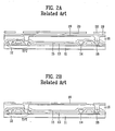
- the anode 18a may be delaminated from the planarization insulating layer 16 while the photoresist is removed.
- the photolithography process and the etch process are performed to separate the anode in the unit of pixel.
- the photoresist 19 is coated on the anode 18 and then a mask 20 is aligned above the transparent substrate 11 such that an edge portion of the pixel is exposed.
- the mask is removed and then the exposed photoresist is developed, so that exposed portions of the photoresist are removed as shown in FIG. 2B.
- the anode material is selectively removed by using the photoresist 19 as a mask, thereby forming the anode 18a. Thereafter, the resultant substrate is loaded into a stripper, so that the photoresist is stripped by a chemical processing in the stripper.
- the anode 18a is delaminated as shown in FIG. 2D due to a processing environment in the stripper and a weak adhesive force between the anode 18a and the planarization insulating layer 16.
- the present invention is directed to a method for fabricating an organic EL device that substantially obviates one or more problems due to limitations and disadvantages of the related art.
- An object of the present invention is to provide a method for fabricating an organic EL device that can prevent delamination of an electrode.
- a method for fabricating an organic EL device including: forming electrode separators on a substrate, the electrode separators being spaced apart by a constant distance from one another; and depositing an electrode material on an entire surface of the substrate including the electrode separators to form an electrode separated by the electrode separators.
- a method for fabricating an organic EL device including: forming a TFT in the unit of pixel on a substrate; forming an insulating layer on an entire surface of the substrate including the TFT; forming an electrode separator on the insulating layer corresponding to the TFT; and depositing an anode material on an entire surface of the insulating layer including the electrode separator to form an anode separated by the electrode separator.
- a method for fabricating an organic EL device including: forming a TFT in the unit of pixel on a substrate; forming an insulating layer on an entire surface of the substrate including the TFT; forming a via-hole penetrating the insulating layer to contact the TFT at a predetermined portion of the insulating layer; forming an electrode separator on a predetermined portion of the insulating layer where an anode is being separated; and depositing an anode material on an entire surface of the insulating layer including the via-hole and the electrode separator to form an anode separated by the electrode separator.
- FIGs. 1A through 1F are sectional views illustrating a process of fabricating an organic EL device according to the related art
- FIGs. 2A through 2D are sectional views illustrating a problem that may be caused in a process of fabricating an organic EL device according to the related art
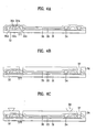
- FIG. 3A through 3E are sectional views illustrating a process of fabricating an organic EL device according to the present invention.
- FIGs. 4A through 4E are sectional views taken along the direction A-A in the processes of FIGs. 3A through 3E;
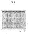
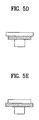
- FIGs. 5A through 5E are sectional views illustrating an electrode separator according to the present invention.
- FIG. 3A through 3E are sectional views illustrating a process of fabricating an organic EL device according to the present invention
- FIGs. 4A through 4E are sectional views taken along the direction A-A in the processes of FIGs. 3A through 3E.
- TFTs 32 are formed in the unit of pixel on a transparent substrate 31.
- amorphous silicon is formed on the transparent substrate 31.
- the amorphous silicon is melted and recrystallized into a poly silicon film by a laser annealing.
- the poly silicon film is patterned by a photolithography process and an etch process, thereby forming an island-shaped semiconductor film 32a.
- a gate insulating layer 32b is formed on an entire surface of a resultant substrate including the semiconductor film 32a, and then a metal film, for example, Chromium (Cr) film is formed on the gate insulating layer 32b.
- a metal film for example, Chromium (Cr) film is formed on the gate insulating layer 32b.
- the metal film is patterned by a photolithography process and an etch process, thereby forming a gate electrode 32c at an area corresponding to and overlapping a center portion of the semiconductor film 32a on the gate insulating layer 32b.
- p-type or n-type impurities are implanted into the semiconductor film 32a using the gate electrode 32c as a mask.
- the impurities-implanted semiconductor film 12a is annealed to activate the implanted impurities, so that a source region 32d and a drain region 32e are formed in the semiconductor film 32a, thereby completing the TFT 32.
- a first insulating layer 33 is formed on an entire surface of a resultant substrate including the TFT 32.
- a contact 34 penetrating the first insulating layer 33 and the gate insulating layer 32b to contact the source electrode 32d and the drain electrode 32e, respectively is formed on the first insulating layer 33, and then a second insulating layer 35 is formed on an entire surface of a resultant substrate including the contact 34.
- a planarization insulating layer 36 is formed on the second insulating layer 35.
- planarization insulating layer 36 and the second insulating layer 35 are selectively removed by a photolithography process and an etch process to form a via-hole 37 exposing a surface of the contact 34 contacting the drain electrode 32e.
- an electrode separator 38 is formed at a portion for separation of the anode (e.g., a boundary between pixels).
- the process for forming the planarization insulating layer 36 may be omitted. If the planarization insulating layer 36 is not formed, the electrode separator 38 is formed on the second insulating layer 35.
- the electrode separator 38 can be formed by various methods, for example, a negative PR process or an etch process.
- the electrode separator 38 is preferably made in a shape that an upper width thereof is larger than a lower width.
- the electrode separator 38 may have an over-hang structure.
- the electrode separator 38 can be made in a reverse trapezoid as shown in FIG. 5A, shapes shown in FIGs. 5B and 5C, or at least two layered shapes shown in FIGs. 5D and 5E.
- the electrode separator 38 is made of at least one selected from the group consisting of organic material, inorganic material, metal and a mixture of them.
- an anode material is deposited on the planarization insulating layer 36 including the electrode separator 38 such that the via-hole 37 is filled with the anode material.
- the anode material includes a conductive material having a high reflectivity, for example, metal such as Cr, Cu, W, Au, Ni, Al, AlNd, Ag, Ti, Ta and the like, alloy of the metals, or a multi-layer film using the same.
- a conductive material having a high reflectivity for example, metal such as Cr, Cu, W, Au, Ni, Al, AlNd, Ag, Ti, Ta and the like, alloy of the metals, or a multi-layer film using the same.
- the electrode separator 38 is formed at the portion to separate the anode and is shaped in a reverse trapezoid, that is, lower width is smaller than upper width. Accordingly, while the anode material is deposited, the anode material is separated centering on the electrode separator 38. As a consequence, the anode 39 is formed on the planarization insulating layer 36.
- the anode material is formed even on the electrode separator 38 as well as on the planarization insulating layer 36.
- the electrode separator 38 due to the existence of the electrode separator 38, the anode material on the electrode separator 38 and the anode material on the planarization insulating layer 36 are automatically separated from each other.
- an insulating layer 40 is formed on a remaining portion except for a real display area of the entire display area.
- the insulating layer may be inorganic insulator or organic insulator.
- SiNx and SiOx are preferable.
- organic insulator as the insulating layer 40, polyimide, polyacryl, and novolac-based material are preferable.
- an organic EL layer is formed on an entire surface of a resultant substrate including the insulating layer 40, and then a cathode is formed on the organic EL layer, thereby completing the organic EL device according to the present invention.
- the method for fabricating an organic EL device according to the present invention has the following effects.
- the anode is automatically separated in the unit of pixels due to the existence of the electrode separator, a separate photolithography process is not needed. Accordingly, delamination of the anode can be prevented, and further product reliability can be enhanced.
Landscapes
- Engineering & Computer Science (AREA)
- Microelectronics & Electronic Packaging (AREA)
- Manufacturing & Machinery (AREA)
- Physics & Mathematics (AREA)
- Optics & Photonics (AREA)
- Electroluminescent Light Sources (AREA)
Abstract
Description
Claims (16)
- A method for fabricating an organic EL device, the method comprising:forming electrode separators on a substrate, the electrode separators being spaced apart by a constant distance from one another; anddepositing an electrode material on an entire surface of the substrate including the electrode separators to form an electrode separated by the electrode separators.
- The method of claim 1, wherein the electrode separator is formed in a shape that an upper width is larger than a lower width.
- The method of claim 1, wherein the electrode separator is made of at least one selected from the group consisting of organic material, inorganic material, metal, and a mixture of them.
- The method of claim 1, wherein the forming the electrode separator comprises at least one of a negative photoresist process and an etch process.
- A method for fabricating an organic EL device, the method comprising:forming a TFT in the unit of pixel on a substrate;forming an insulating layer on an entire surface of the substrate including the TFT;forming an electrode separator on the insulating layer corresponding to the TFT; anddepositing an anode material on an entire surface of the insulating layer including the electrode separator to form an anode separated by the electrode separator.
- The method of claim 5, wherein the electrode separator is formed in a shape that an upper width is larger than a lower width.
- The method of claim 5, wherein the electrode separator is made of at least one selected from the group consisting of organic material, inorganic material, metal, and a mixture of them.
- The method of claim 5, wherein the forming the electrode separator comprises at least one of a negative photoresist process and an etch process.
- A method for fabricating an organic EL device, the method comprising:forming a TFT in the unit of pixel on a substrate;forming an insulating layer on an entire surface of the substrate including the TFT;forming a via-hole penetrating the insulating layer to contact the TFT at a predetermined portion of the insulating layer;forming an electrode separator on a predetermined portion of the insulating layer where an anode is being separated; anddepositing an anode material on an entire surface of the insulating layer including the via-hole and the electrode separator to form an anode separated by the electrode separator.
- The method of claim 9, wherein the electrode separator is formed in a shape that an upper width is larger than a lower width.
- The method of claim 9, wherein the electrode separator has an over-hang structure.
- The method of claim 9, wherein the electrode separator is shaped in a reverse trapezoid.
- The method of claim 9, wherein the electrode separator comprises at least two layers.
- The method of claim 9, wherein the electrode separator is made of at least one selected from the group consisting of organic material, inorganic material, metal, and a mixture of them.
- The method of claim 9, wherein the forming the electrode separator comprises at least one of a negative photoresist process and an etch process.
- The method of claim 9, further comprising:forming a second insulating layer at a portion except for an emission area of each pixel after forming the anode; andsequentially forming an organic EL layer and a cathode on an entire surface of the anode including the second insulating layer.
Applications Claiming Priority (2)
| Application Number | Priority Date | Filing Date | Title |
|---|---|---|---|
| KR1020030090167A KR100587340B1 (en) | 2003-12-11 | 2003-12-11 | Manufacturing method of organic EL element |
| KR2003090167 | 2003-12-11 |
Publications (3)
| Publication Number | Publication Date |
|---|---|
| EP1542283A2 true EP1542283A2 (en) | 2005-06-15 |
| EP1542283A3 EP1542283A3 (en) | 2006-07-26 |
| EP1542283B1 EP1542283B1 (en) | 2011-06-15 |
Family
ID=34511211
Family Applications (1)
| Application Number | Title | Priority Date | Filing Date |
|---|---|---|---|
| EP04029332A Expired - Lifetime EP1542283B1 (en) | 2003-12-11 | 2004-12-10 | Organic electroluminescent device and its method of fabrication |
Country Status (5)
| Country | Link |
|---|---|
| US (1) | US7579040B2 (en) |
| EP (1) | EP1542283B1 (en) |
| JP (1) | JP3981838B2 (en) |
| KR (1) | KR100587340B1 (en) |
| CN (1) | CN100481485C (en) |
Families Citing this family (11)
| Publication number | Priority date | Publication date | Assignee | Title |
|---|---|---|---|---|
| US20070128401A1 (en) * | 2005-12-05 | 2007-06-07 | Wintek Corporation | Electrode separator |
| JP5019644B2 (en) * | 2010-03-24 | 2012-09-05 | 株式会社ジャパンディスプレイセントラル | Organic EL device |
| US8922463B2 (en) * | 2010-04-26 | 2014-12-30 | Samsung Display Co., Ltd. | Organic light-emitting display apparatus |
| KR101351512B1 (en) * | 2010-10-25 | 2014-01-16 | 엘지디스플레이 주식회사 | Organic Light Emitting Diode and Method for fabricating the same |
| WO2015171849A2 (en) | 2014-05-07 | 2015-11-12 | Open Water Power, Incorporated | Hydrogen management in electrochemical systems |
| US9816860B2 (en) | 2014-08-22 | 2017-11-14 | Spectrasensors, Inc. | Spectrometer with active beam steering |
| US9518866B2 (en) | 2014-08-22 | 2016-12-13 | Spectrasensors, Inc. | Spectrometer with variable beam power and shape |
| US10024788B2 (en) | 2015-05-04 | 2018-07-17 | Spectrasensors, Inc. | Spectrometer with random beam profiles |
| CN105118929B (en) * | 2015-08-03 | 2018-01-02 | 京东方科技集团股份有限公司 | Electrode structure and organic light-emitting units and its manufacture method |
| US12550534B2 (en) | 2021-08-11 | 2026-02-10 | Yunnan Invensight Optoelectronics Technology Co., Ltd. | Display substrate and electronic apparatus having concave points within gap between pixel regions |
| US12302710B2 (en) | 2021-08-11 | 2025-05-13 | Yunnan Invensight Optoelectronics Technology Co., Ltd. | Display substrate and electronic apparatus |
Family Cites Families (8)
| Publication number | Priority date | Publication date | Assignee | Title |
|---|---|---|---|---|
| US5701055A (en) * | 1994-03-13 | 1997-12-23 | Pioneer Electronic Corporation | Organic electoluminescent display panel and method for manufacturing the same |
| JP3813217B2 (en) | 1995-03-13 | 2006-08-23 | パイオニア株式会社 | Method for manufacturing organic electroluminescence display panel |
| JP3900769B2 (en) | 1999-01-26 | 2007-04-04 | 三菱化学株式会社 | Method for manufacturing organic electroluminescent device |
| JP4434411B2 (en) * | 2000-02-16 | 2010-03-17 | 出光興産株式会社 | Active drive type organic EL light emitting device and manufacturing method thereof |
| TW461228B (en) * | 2000-04-26 | 2001-10-21 | Ritdisplay Corp | Method to manufacture the non-photosensitive polyimide pixel definition layer of organic electro-luminescent display panel |
| JP2002083691A (en) * | 2000-09-06 | 2002-03-22 | Sharp Corp | Active matrix driven organic LED display device and method of manufacturing the same |
| US6664730B2 (en) | 2001-07-09 | 2003-12-16 | Universal Display Corporation | Electrode structure of el device |
| JP2003109773A (en) | 2001-07-27 | 2003-04-11 | Semiconductor Energy Lab Co Ltd | Light emitting device, semiconductor device, and manufacturing method thereof |
-
2003
- 2003-12-11 KR KR1020030090167A patent/KR100587340B1/en not_active Expired - Lifetime
-
2004
- 2004-12-10 EP EP04029332A patent/EP1542283B1/en not_active Expired - Lifetime
- 2004-12-10 US US11/008,788 patent/US7579040B2/en active Active
- 2004-12-10 JP JP2004358621A patent/JP3981838B2/en not_active Expired - Lifetime
- 2004-12-13 CN CNB2004100988084A patent/CN100481485C/en not_active Expired - Lifetime
Also Published As
| Publication number | Publication date |
|---|---|
| CN1627872A (en) | 2005-06-15 |
| EP1542283B1 (en) | 2011-06-15 |
| EP1542283A3 (en) | 2006-07-26 |
| KR100587340B1 (en) | 2006-06-08 |
| JP3981838B2 (en) | 2007-09-26 |
| JP2005174940A (en) | 2005-06-30 |
| US7579040B2 (en) | 2009-08-25 |
| US20050129840A1 (en) | 2005-06-16 |
| CN100481485C (en) | 2009-04-22 |
| KR20050057940A (en) | 2005-06-16 |
Similar Documents
| Publication | Publication Date | Title |
|---|---|---|
| US20240284739A1 (en) | Display apparatus and method of manufacturing display apparatus | |
| US8227803B2 (en) | Organic electroluminescent display device and method for fabricating the same | |
| CN107689389B (en) | Organic Light Emitting Diode Display Device | |
| US7227184B2 (en) | Active matrix organic electro luminescence display device and manufacturing method for the same | |
| US8698251B2 (en) | Organic light emitting diode display and method of manufacturing the same | |
| US20200161569A1 (en) | Flexible amoled substrate and manufacturing method thereof | |
| US20110003414A1 (en) | Organic light emitting diode display and fabricating method thereof | |
| US10069112B2 (en) | Organic light emitting diode display device | |
| KR20130107459A (en) | Oganic electro-luminesence display panel and manufactucring metod of the same | |
| US7579040B2 (en) | Method for fabricating organic electro-luminance device | |
| KR20150057016A (en) | Organic electro luminescent device and method of fabricating the same | |
| CN100463213C (en) | Organic electroluminescence device and manufacturing method thereof | |
| US20190198594A1 (en) | Display apparatus and method of manufacturing the same | |
| US8987723B2 (en) | Display device and method of manufacturing the same | |
| KR101572268B1 (en) | Organic electroluminescent device and manufacturing method thereof | |
| JP2004111361A (en) | Active matrix organic electroluminescent device and method of manufacturing the same | |
| CN116264792A (en) | Electroluminescence display device | |
| KR101849575B1 (en) | Organic electro-luminesence display panel and manufactucring method of the same | |
| US8564194B2 (en) | Organic light emitting diode device and method for fabricating the same | |
| GB2626688A (en) | Electroluminescent display device | |
| CN111769138A (en) | Array substrate and manufacturing method thereof | |
| KR100635070B1 (en) | Organic electroluminescent device and manufacturing method thereof |
Legal Events
| Date | Code | Title | Description |
|---|---|---|---|
| PUAI | Public reference made under article 153(3) epc to a published international application that has entered the european phase |
Free format text: ORIGINAL CODE: 0009012 |
|
| 17P | Request for examination filed |
Effective date: 20041210 |
|
| AK | Designated contracting states |
Kind code of ref document: A2 Designated state(s): AT BE BG CH CY CZ DE DK EE ES FI FR GB GR HU IE IS IT LI LT LU MC NL PL PT RO SE SI SK TR |
|
| AX | Request for extension of the european patent |
Extension state: AL BA HR LV MK YU |
|
| PUAL | Search report despatched |
Free format text: ORIGINAL CODE: 0009013 |
|
| AK | Designated contracting states |
Kind code of ref document: A3 Designated state(s): AT BE BG CH CY CZ DE DK EE ES FI FR GB GR HU IE IS IT LI LT LU MC NL PL PT RO SE SI SK TR |
|
| AX | Request for extension of the european patent |
Extension state: AL BA HR LV MK YU |
|
| 17Q | First examination report despatched |
Effective date: 20070129 |
|
| AKX | Designation fees paid |
Designated state(s): DE FR GB NL |
|
| RAP1 | Party data changed (applicant data changed or rights of an application transferred) |
Owner name: LG DISPLAY CO., LTD. |
|
| GRAP | Despatch of communication of intention to grant a patent |
Free format text: ORIGINAL CODE: EPIDOSNIGR1 |
|
| RIC1 | Information provided on ipc code assigned before grant |
Ipc: H01L 27/32 20060101AFI20101214BHEP |
|
| RTI1 | Title (correction) |
Free format text: ORGANIC ELECTROLUMINESCENT DEVICE AND ITS METHOD OF FABRICATION |
|
| GRAS | Grant fee paid |
Free format text: ORIGINAL CODE: EPIDOSNIGR3 |
|
| GRAA | (expected) grant |
Free format text: ORIGINAL CODE: 0009210 |
|
| AK | Designated contracting states |
Kind code of ref document: B1 Designated state(s): DE FR GB NL |
|
| REG | Reference to a national code |
Ref country code: GB Ref legal event code: FG4D |
|
| REG | Reference to a national code |
Ref country code: DE Ref legal event code: R096 Ref document number: 602004033038 Country of ref document: DE Effective date: 20110721 |
|
| REG | Reference to a national code |
Ref country code: NL Ref legal event code: VDEP Effective date: 20110615 |
|
| PG25 | Lapsed in a contracting state [announced via postgrant information from national office to epo] |
Ref country code: NL Free format text: LAPSE BECAUSE OF FAILURE TO SUBMIT A TRANSLATION OF THE DESCRIPTION OR TO PAY THE FEE WITHIN THE PRESCRIBED TIME-LIMIT Effective date: 20110615 |
|
| PLBE | No opposition filed within time limit |
Free format text: ORIGINAL CODE: 0009261 |
|
| STAA | Information on the status of an ep patent application or granted ep patent |
Free format text: STATUS: NO OPPOSITION FILED WITHIN TIME LIMIT |
|
| 26N | No opposition filed |
Effective date: 20120316 |
|
| REG | Reference to a national code |
Ref country code: DE Ref legal event code: R097 Ref document number: 602004033038 Country of ref document: DE Effective date: 20120316 |
|
| REG | Reference to a national code |
Ref country code: FR Ref legal event code: PLFP Year of fee payment: 12 |
|
| REG | Reference to a national code |
Ref country code: FR Ref legal event code: PLFP Year of fee payment: 13 |
|
| REG | Reference to a national code |
Ref country code: FR Ref legal event code: PLFP Year of fee payment: 14 |
|
| REG | Reference to a national code |
Ref country code: FR Ref legal event code: PLFP Year of fee payment: 15 |
|
| REG | Reference to a national code |
Ref country code: DE Ref legal event code: R079 Ref document number: 602004033038 Country of ref document: DE Free format text: PREVIOUS MAIN CLASS: H01L0027320000 Ipc: H10K0059000000 |
|
| PGFP | Annual fee paid to national office [announced via postgrant information from national office to epo] |
Ref country code: GB Payment date: 20231023 Year of fee payment: 20 |
|
| PGFP | Annual fee paid to national office [announced via postgrant information from national office to epo] |
Ref country code: FR Payment date: 20231024 Year of fee payment: 20 Ref country code: DE Payment date: 20231023 Year of fee payment: 20 |
|
| REG | Reference to a national code |
Ref country code: DE Ref legal event code: R071 Ref document number: 602004033038 Country of ref document: DE |
|
| REG | Reference to a national code |
Ref country code: GB Ref legal event code: PE20 Expiry date: 20241209 |
|
| PG25 | Lapsed in a contracting state [announced via postgrant information from national office to epo] |
Ref country code: GB Free format text: LAPSE BECAUSE OF EXPIRATION OF PROTECTION Effective date: 20241209 |
|
| PG25 | Lapsed in a contracting state [announced via postgrant information from national office to epo] |
Ref country code: GB Free format text: LAPSE BECAUSE OF EXPIRATION OF PROTECTION Effective date: 20241209 |