EP1542268A1 - Method of dry etching, dry etching gas and process for producing perfluoro-2-pentyne - Google Patents
Method of dry etching, dry etching gas and process for producing perfluoro-2-pentyne Download PDFInfo
- Publication number
- EP1542268A1 EP1542268A1 EP03764209A EP03764209A EP1542268A1 EP 1542268 A1 EP1542268 A1 EP 1542268A1 EP 03764209 A EP03764209 A EP 03764209A EP 03764209 A EP03764209 A EP 03764209A EP 1542268 A1 EP1542268 A1 EP 1542268A1
- Authority
- EP
- European Patent Office
- Prior art keywords
- dry etching
- pentene
- pentyne
- fluorine
- perfluoro
- Prior art date
- Legal status (The legal status is an assumption and is not a legal conclusion. Google has not performed a legal analysis and makes no representation as to the accuracy of the status listed.)
- Withdrawn
Links
Classifications
-
- H—ELECTRICITY
- H10—SEMICONDUCTOR DEVICES; ELECTRIC SOLID-STATE DEVICES NOT OTHERWISE PROVIDED FOR
- H10P—GENERIC PROCESSES OR APPARATUS FOR THE MANUFACTURE OR TREATMENT OF DEVICES COVERED BY CLASS H10
- H10P50/00—Etching of wafers, substrates or parts of devices
- H10P50/20—Dry etching; Plasma etching; Reactive-ion etching
- H10P50/24—Dry etching; Plasma etching; Reactive-ion etching of semiconductor materials
- H10P50/242—Dry etching; Plasma etching; Reactive-ion etching of semiconductor materials of Group IV materials
-
- H—ELECTRICITY
- H10—SEMICONDUCTOR DEVICES; ELECTRIC SOLID-STATE DEVICES NOT OTHERWISE PROVIDED FOR
- H10P—GENERIC PROCESSES OR APPARATUS FOR THE MANUFACTURE OR TREATMENT OF DEVICES COVERED BY CLASS H10
- H10P50/00—Etching of wafers, substrates or parts of devices
- H10P50/20—Dry etching; Plasma etching; Reactive-ion etching
- H10P50/26—Dry etching; Plasma etching; Reactive-ion etching of conductive or resistive materials
- H10P50/264—Dry etching; Plasma etching; Reactive-ion etching of conductive or resistive materials by chemical means
- H10P50/266—Dry etching; Plasma etching; Reactive-ion etching of conductive or resistive materials by chemical means by vapour etching only
- H10P50/267—Dry etching; Plasma etching; Reactive-ion etching of conductive or resistive materials by chemical means by vapour etching only using plasmas
-
- C—CHEMISTRY; METALLURGY
- C07—ORGANIC CHEMISTRY
- C07C—ACYCLIC OR CARBOCYCLIC COMPOUNDS
- C07C17/00—Preparation of halogenated hydrocarbons
- C07C17/25—Preparation of halogenated hydrocarbons by splitting-off hydrogen halides from halogenated hydrocarbons
-
- C—CHEMISTRY; METALLURGY
- C07—ORGANIC CHEMISTRY
- C07C—ACYCLIC OR CARBOCYCLIC COMPOUNDS
- C07C17/00—Preparation of halogenated hydrocarbons
- C07C17/26—Preparation of halogenated hydrocarbons by reactions involving an increase in the number of carbon atoms in the skeleton
- C07C17/263—Preparation of halogenated hydrocarbons by reactions involving an increase in the number of carbon atoms in the skeleton by condensation reactions
- C07C17/2637—Preparation of halogenated hydrocarbons by reactions involving an increase in the number of carbon atoms in the skeleton by condensation reactions between a compound containing only oxygen and possibly halogen as hetero-atoms and a halogenated hydrocarbon
-
- C—CHEMISTRY; METALLURGY
- C07—ORGANIC CHEMISTRY
- C07C—ACYCLIC OR CARBOCYCLIC COMPOUNDS
- C07C21/00—Acyclic unsaturated compounds containing halogen atoms
- C07C21/02—Acyclic unsaturated compounds containing halogen atoms containing carbon-to-carbon double bonds
- C07C21/18—Acyclic unsaturated compounds containing halogen atoms containing carbon-to-carbon double bonds containing fluorine
-
- C—CHEMISTRY; METALLURGY
- C07—ORGANIC CHEMISTRY
- C07C—ACYCLIC OR CARBOCYCLIC COMPOUNDS
- C07C21/00—Acyclic unsaturated compounds containing halogen atoms
- C07C21/22—Acyclic unsaturated compounds containing halogen atoms containing carbon-to-carbon triple bonds
-
- H—ELECTRICITY
- H10—SEMICONDUCTOR DEVICES; ELECTRIC SOLID-STATE DEVICES NOT OTHERWISE PROVIDED FOR
- H10P—GENERIC PROCESSES OR APPARATUS FOR THE MANUFACTURE OR TREATMENT OF DEVICES COVERED BY CLASS H10
- H10P50/00—Etching of wafers, substrates or parts of devices
- H10P50/20—Dry etching; Plasma etching; Reactive-ion etching
- H10P50/28—Dry etching; Plasma etching; Reactive-ion etching of insulating materials
- H10P50/282—Dry etching; Plasma etching; Reactive-ion etching of insulating materials of inorganic materials
- H10P50/283—Dry etching; Plasma etching; Reactive-ion etching of insulating materials of inorganic materials by chemical means
Definitions
- This invention relates to a method of dry etching, a dry etching gas, and a process for producing perfluoro-2-pentyne. More particularly, this invention relates to a method of dry etching wherein an etching rate is high, a selectivity for substrate is high, and a fine pattern having a minimum line width of not more than 200 nm can be formed on a silicon substrate at an enhanced stability; a dry etching gas; and a process for producing perfluoro-2-pentyne used for the dry etching.
- Fluorine-containing compounds having an unsaturated bond are disclosed in Japanese Unexamined Patent Publication H9-191002. It is reported in this patent publication that evaluation of etching was conducted on a resist pattern formed with radiation having a wavelength of 300 nm by a KrF excima laser lithography, and good results were obtained. In Japanese Unexamined Patent Publication 2002-184768, it is reported that evaluation of etching was conducted on a resist pattern formed by lithography using deep UV, namely, ultraviolet rays of a wavelength of 200 to 300 nm, and good results were obtained.
- a resist formed from a high molecular weight compound having an aromatic ring structure For the exposure to radiation with a wavelength of at least 200 nm, for example, irradiation using a KrF with a wavelength of 248 nm, a resist formed from a high molecular weight compound having an aromatic ring structure has heretofore been widely used. This is because a resist formed from a high molecular weight compound having an aromatic ring structure exhibits a high resistance for dry etching, and, at an etching step after light exposure and development, a high etching selectivity for silicon oxide substrate can be obtained. However, a resist pattern having a minimum line width of 210 nm can be obtained at the utmost with a KrF (248 nm) excima laser used for 256 megabit DRAM.
- an ArF (193 nm) excima laser or other light sources of shorter wavelength should be used for the production of DRAM with 1 gigabit or more.
- a fine pattern cannot be formed when radiation with a wavelength of 200 nm or less such as ArF (193 nm) laser or X-rays is used, because radiation is absorbed to an undue extent by an aromatic ring.
- a protective coating such as polysilicon as well as an unexposed area of a photoresist tend to be undesirably etched, and thus, the etching selectivity for silicon oxide is not high and a fine pattern is difficult to form.
- a resist formed on a substrate represented by silicon oxide film becomes thinner, and therefore, a high etching selectivity becomes more difficult to attain.
- An object of the present invention is to provide a method of dry etching by which a high etching rate and a high etching selectivity can be attained and a fine resist pattern with a minimum line width of 200 nm or less can be formed with good stability, even for a resist having poor resistance to dry etching using a light source with a short wavelength of 195 nm or less.
- Another object of the present invention is to provide a dry etching gas by which a high etching rate and a high etching selectivity can be attained and a fine resist pattern with a minimum line width of 200 nm or less can be formed with good stability, even for a resist having poor resistance to dry etching using a light source with a short wavelength of 195 nm or less.
- a further object of the present invention is to provide a process for producing perfluoro-2-pentyne which is suitable for use as the above-mentioned dry etching gas.
- the inventors made an extensive research for achieving the above-mentioned objects, and found that, in the case when dry etching is carried out using a fluorine-containing compound having 4 to 6 carbon atoms and at least one unsaturated bond as an etching gas, a high etching selectivity can be attained without reduction of etching rate, even for a resist having poor resistance to dry etching. Based on this finding, the present invention has been completed.
- a dry etching method characterized in that a resist film formed on a substrate is irradiated with radiation having a wavelength of not more than 195 nm to form a resist pattern having a minimum line width of not more than 200 nm, and the substrate having the resist pattern formed thereon is subjected to dry etching using a fluorine-containing compound having 4 to 6 carbon atoms and at least one unsaturated bond as an etching gas.
- a dry etching gas comprised of a fluorine-containing compound having 4 to 6 carbon atoms and at least one unsaturated bond, and used for dry etching for a resist film forming a resist pattern having a minimum line width of not more than 200 nm at irradiation with radiation having a wavelength of not more than 195 nm.
- a process for producing perfluoro-2-pentyne characterized in that a 1,1,1-trihalo-2,2,2-trifluoroethane is allowed to react with pentafluoropropionaldehyde to give a 2-halo-1,1,1,4,4,5,5,5-octafluoro-2-pentene, and the thus-produced 2-halo-1,1,1,4,4,5,5,5-octafluoro-2-pentene is dehydrohalogenated.
- a resist film formed on a substrate is irradiated with radiation having a wavelength of not more than 195 nm to form a resist pattern having a minimum line width of not more than 200 nm, and then, the substrate having the resist pattern thus-formed thereon is subjected to dry etching using a fluorine-containing compound having 4 to 6 carbon atoms and at least one unsaturated bond as an etching gas.
- a fine pattern of a minimum line width of not more than 200 nm, preferably not more than 180 nm, more preferably not more than 150 nm and especially preferably not more than 140 nm can be easily formed with a high precision.
- minimum line width we mean broadly those which include, for example, a diameter of contact holes in the case when the resist pattern is contact holes.
- a fluorine-containing compound having at least one unsaturated bond, but having three or less carbon atoms is used as a dry etching gas, the selectivity in dry etching tends to be reduced.
- a fluorine-containing compound having at least one unsaturated bond but having at least 7 carbon atoms is usually difficult to use as a dry etching because it has a high boiling point.
- the resist film formed on a substrate is not particularly limited, but is preferably formed from a high molecular weight compound containing 0% to 10% by weight of repeating units having an aromatic ring structure.
- the content of repeating units having an aromatic ring structure in the high molecular weight compound constituting the resist film is more preferably in the range of 0% to 5% by weight, especially 0% to 2% by weight.
- the content of repeating units having an aromatic ring structure in the high molecular weight compound constituting the resist film is in the range of 0% to 10% by weight, transparency to radiation with a wavelength of not more than 195 nm can be obtained and a desired resist pattern having a minimum line width of not more than 200 nm can be formed.
- the high molecular weight compound containing 0% to 10% by weight of repeating units having an aromatic ring structure there can be mentioned a partially hydrogenated resin product of a p-hydroxystyrene/t-butyl methacrylate copolymer, a partially hydrogenated resin product of a p-hydroxystyrene/4-ethenylphenoxyacetic acid 1-alkylcyclohexyl ester copolymer, an isobornyl methacrylate/methyl methacrylate/t-butyl methacrylate/methacrylic acid quaternary polymer, an adamantyl methacrylate/t-butyl methacrylate copolymer resin, a valerolactone metacrylic acid ester/2-alkyladamantyl methacrylate/hydroxyadamantyl methacrylate terpolymer resin, a t-butyl methacrylate/vinyl alkyl ether/maleic anhydride ter
- the procedure for forming a resist film on a substrate is not particularly limited and the conventional procedure may be adopted.
- a solution of a resist composition is applied onto a substrate by spin coating or other coating means, and then a solvent is removed by evaporation from the coating solution to be thereby dried. According to the need, the dried coating is pre-baked.
- an acid generator such as an onium salt, diazomethane derivatives and glyoxime derivatives can be incorporated according to the need.
- the radiation used in the present invention has a wavelength of not more than 195 nm, preferably not more than 170 nm especially preferably not more than 150 nm.
- the radiation is not particularly limited provided that it has a wavelength of not more than 195 nm.
- ArF excima laser 1942 nm
- F 2 excima laser 157 nm
- Kr 2 excima laser 146 nm
- KrAr excima laser 134 nm
- AR 2 excima laser 126 nm
- vacuum ultraviolet rays not more than 170 nm
- electron beam (EB) and X rays X rays.
- the procedure for forming a resist pattern is also not particularly limited.
- a resist film is masked and irradiated with radiation according to the pattern. Then the irradiated resist is post-baked according to the need, and development is carried out using an aqueous alkali such as an aqueous tetramethylammonium hydroxide solution to form a resist pattern, followed by dry etching.
- an aqueous alkali such as an aqueous tetramethylammonium hydroxide solution
- a fluorine-containing compound having 4 to 6 carbon atoms and at least one unsaturated bond is used as a dry etching gas.
- fluorine-containing compound we mean a compound composed of carbon and fluorine or a compound composed of carbon, hydrogen and fluorine.
- the unsaturated bond may be either a double bond or a triple bond.
- the fluorine-containing compound may have both a double bond and a triple bond.
- fluorine-containing compound having a triple bond there can be mentioned perfuoro-1-butyne, perfuoro-2-butyne, perfuoro-1-pentyne, perfuoro-2-pentyne, perfuoro-1,3-pentadiyne, perfuoro-1,4-pentadiyne, perfuoro-1-hexyne, perfuoro-2-hexyne, perfuoro-3-hexyne, perfuoro-1,3-hexadiyne, perfuoro-1,4-hexadiyne, perfuoro-1,5-hexadiyne and perfuoro-2,4-hexadiyne.
- fluorine-containing compound having a double bond there can be mentioned perfuoro-1-butene, perfuoro-2-butene, perfuoro-1,3-butadiene, perfuoro-1-pentene, perfuoro-2-pentene, perfuoro-1,3-pentadiene, perfuoro-1,4-pentadiene, perfuoro-2-methyl-1,3-butadiene, octafluorocyclopentene, hexafluorocyclopentadiene, perfluoro-1-hexene, perfluoro-2-hexene, perfluoro-3-hexene, perfluoro-1,3-hexadiene, perfluoro-1,4-hexadiene, perfluoro-1,5-hexadiene, perfluoro-2,4-hexadiene, perfluoro-1,3,5-hexatrien
- fluorine-containing compound having both of a double bond and a triple bond there can be mentioned perfuoro-1-buten-3-yne, perfuoro-1-penten-3-yne, perfuoro-1-penten-4-yne, perfuoro-3-penten-1-yne, perfuoro-2-methyl-1-buten-3-yne, perfuoro-1-cyclohexen-3-yne and perfuoro-1-cyclohexen-4-yne.
- the above-mentioned fluorine-containing compound having at least one unsaturated bond may be used either alone or as a combination of at least two thereof as a dry etching gas.
- fluorine-containing compounds perfluoro-2-butyne, perfluoro-2-pentyne, perfuoro-2-hexyne, perfluoro-3-hexyne, 1,1,1,2,4,4,5,5,5-nonafluoro-2-pentene, 1,1,1,3,4,4,5,5,5-nonafluoro-2-pentene and perfuoro-2-pentene are preferable because of high stability.
- 1,1,1,2,4,4,5,5,5-nonafluoro-2-pentene, 1,1,1,3,4,4,5,5,5-nonafluoro-2-pentene and perfuoro-2-pentene are especially preferable.
- Perfluoro-2-pentyne and perfluoro-2-butyne are preferable in view of high etching rate and high etching selectivity. Perfluoro-2-pentyne is especially preferable.
- the fluorine-containing compound having 4 to 6 carbon atoms and at least one unsaturated bond preferably has a purity of at least 90% by volume, more preferably at least 99% by volume and especially preferably at least 99.9% by volume. If the fluorine-containing compound has a purity of lower than 90% by volume, the etching rate and the etching selectivity are liable to be poor.
- a material to be etched includes, for example, silicon oxide, silicon nitride, aluminum, tungsten, molybdenum, tantalum, titanium, chromium, chromium oxide and gold.
- silicon wafer having silicon oxide film or aluminum film As specific examples of the substrate to be etched, there can be mentioned silicon wafer having silicon oxide film or aluminum film.
- the size of silicon wafer is not particularly limited, but the silicon wafer usually has a size of 8 inches or 12 inches.
- etching is carried out preferably under irradiation with a plasma.
- the plasma preferably has a density of at least 10 10 ions/cm 3 , more preferably in the range of 10 10 to 10 13 ions/cm 3 .
- the plasma density is in the range of 10 10 to 10 13 ions/cm 3 , higher etching rate and higher etching selectivity can be obtained and a fine pattern can be formed.
- an apparatus for generating plasma there can be mentioned those which are of a helicon wave type, a high-frequency induction type, a parallel flat plate type and a magnetron type. Of these, a helicon wave type apparatus and a high-frequency induction type apparatus are preferable because a plasma having a high density region can be easily generated.
- the fluorine-containing compound having 4 to 6 carbon atoms and at least one unsaturated bond is preferably introduced into an apparatus vacuumed to an extent such that the inner pressure reaches a pressure in the range of 0.0013 to 1,300 Pa, more preferably 0.13 to 1.3 Pa.
- the temperature which the substrate to be dry-etched reaches during the dry etching step is preferably in the range of 0 to 300°C, more preferably 60 to 250°C and especially preferably 80 to 200°C.
- the treating time for the dry etching is usually in the range of 10 seconds to 10 minutes. However, etching can be effected at a high etching rate in the dry etching method of the present invention, and therefore, the dry etching can be carried out for a treating time of 10 seconds to 3 minutes with a high productivity.
- the gas used in combination with the fluorine-containing compound includes, for example, rare gases such as helium, neon, argon, krypton and xenon; and oxygen and oxygen-containing gases such as carbon monoxide and carbon dioxide. Of these, oxygen is preferably used in combination with the fluorine-containing compound because oxygen has a dissociation accelerating action for an etching gas.
- the dry etching gas used in the present invention is comprised of a fluorine-containing compound having 4 to 6 carbon atoms and at least one unsaturated bond, with which dry etching is carried out for a resist pattern having a minimum line width of not more than 200 nm formed by irradiation with radiation with a wavelength of not more than 195 nm.
- a fluorine-containing gas having 4 to 6 carbon atoms various gases can be used as mentioned above.
- Perfluoro-2-pentyne is especially preferably used because high etching rate and high etching selectivity can be obtained.
- a 1,1,1-trihalo-2,2,2-trifluoroethane is allowed to react with pentafluoropropionaldehyde to give a 2-halo-1,1,1,4,4,5,5,5-octafluoro-2-pentene, and the thus-produced 2-halo-1,1,1,4,4,5,5,5-octafluoro-2-pentene is dehydrohalogenated to give perfluoro-2-pentyne.
- the conditions for allowing a 1,1,1-trihalo-2,2,2-trifluoroethane to react with pentafluoropropionaldehyde are not particularly limited.
- pentafluoropropionaldehyde hydrate is treated with a dehydrating agent such as phosphorus pentoxide under heated conditions to be thereby dehydrated to give pentafluoropropionaldehyde, and the pentafluoropropionaldehyde is blown in a cooled polar solvent such as dimethylformamide to give a solution.
- a 1,1,1-trihalo-2,2,2-trifluoroethane and powdery zinc oxide were added, and the mixture is heated to give a 2-halo-1,1,1,4,4,5,5,5-octafluoro-2-pentene.
- the amount of pentafluoropropionaldehyde hydrate used is preferably in the range of 1 to 2 moles, more preferably 1.2 to 1.5 moles, per mole of a 1,1,1-trihalo-2,2,2-trifluoroethane to be reacted with a dehydrated product of the pentafluoropropionaldehyde hydrate.
- the amount of powdery zinc added is preferably in the range of 2 to 3 moles, more preferably 2.2 to 2.5 moles, per mole of the 1,1,1-trihalo-2,2,2-trifluoroethane.
- Powdery zinc oxide is preferably previously activated by treating with, for example, dilute aqueous hydrochloric acid or acetic anhydride prior to the addition to the pentafluoropropionaldehyde solution.
- a preferable example of the starting material, 1,1,1-trihalo- 2,2,2-trifluoroethane is 1,1,1-trichloro-2,2,2-trifluoroethane.
- the reaction temperature is usually in the range of room temperature to 150°C, more preferably 50°C to 100°C.
- the reaction time is usually in the range of 1 to 20 hours, more preferably 3 to 10 hours.
- An after-treatment for the above-mentioned reaction may be conventional. That is, the reaction is stopped by adding dilute hydrochloric acid to the reaction liquid, and the reaction product is extracted with an extract solvent such as ethyl acetate or diethyl ether, neutralized with a saturated aqueous sodium bicarbonate solution, and then dried over a desiccating agent such as sodium sulfate. The dried product is concentrated by a rotary evaporator to give a crude purified product.
- the crude purified product may be subjected to the dehydrohalogenation, or, may be distilled for purification and then subjected to the dehydrohalogenation.
- a basic compound such as, for example, potassium hydroxide is added to the obtained 2-halo-1,1,1,4,4,5,5,5-octafluoro-2-pentene whereby dehydrohalogenation is effected to produce a triple bond, namely, give perfluoro-2-pentyne.
- a pressure-resistant autoclave is charged with a basic compound and the 2-halo-1,1,1,4,4,5,5,5-octafluoro-2-pentene, and the content is heated, and a gaseous product produced by the reaction is collected in a cooled trap.
- a procedure utilizing a feature such that perfluoro-2-pentyne to be produced has a boiling point of 5°C can be adopted. That is, a reactor is previously charged with a basic compound, and, while the content was stirred, the 2-halo-1,1,1,4,4,5,5,5-octafluoro-2-pentene was dropwise added and a gaseous product produced by the reaction is collected in a cooled trap.
- the amount of basic compound used is preferably in the range of 1 to 10 moles, more preferably 2 to 5 moles, per mole of the 2-halo-1,1,1,4,4,5,5,5-octafluoro-2-pentene.
- the reaction temperature is usually in the range of room temperature to 250°C, more preferably 50°C to 200°C.
- the collected perfluoro-2-pentyne can be subjected to distillation for enhancing the purity.
- perfluoro-2-pentyne having a high purity can be produced with an enhanced efficiency from a readily available raw material, as compared with heretofore proposed processes for producing perfluoro-2-pentyne, which include dechlorination of 2,3-dichloro-1,1,1,4,4,5,5,5-octafluoro-2-pentene by using zinc, isomerization of perfluoropentadiene, or dehydrofluorination of 1,1,1,2,3,4,4,5,5,5-decafluoropentane.
- selectivity ratio in etching was calculated by the following equation.
- Hastelloy An autoclave made of Hastelloy was charged with 394 parts of commercially available palletized potassium hydroxide (purity: 85% by weight) and 300 parts of 1,1,1,2,3,4,4,5,5,5-decafluoropentane ("VertrelTM XF" available from Du pont). The content was thoroughly stirred and a reaction was carried out at 200°C for 7.5 hours.
- the autoclave was cooled, and then, in order for distilling and collecting the thus-produced reaction mixture, a condenser and a vacuum pump were connected to the autoclave.
- the reaction mixture was collected into the condenser, which was cooled under a reduced pressure by liquid nitrogen, to give 182.5 parts of a reaction product.
- Analysis of the reaction product by gas chromatography revealed that it contained perfluoro-2-pentyne (target product), 1,1,1,2,4,4,5,5,5-nonafluoro-2-pentene, 1,1,1,3,4,4,5,5,5-nonafluoro-2-pentene and a small amount of 1,1,1,2,3,4,4,5,5,5-decafluoropentane (raw material).
- the yield of the target product was 20.6% by weight based on the amount of the raw material charged. A great portion of the unreacted raw material was decomposed and polymerized, which remained within the autoclave, and thus, the reaction product contained only about 1% by weight of raw material.
- Ten parts of a terpolymer comprised of 5-norbornene-2-methanol units, maleic anhydride units and t-butyl methacrylate units (copolymerization ratio: 1:1:1 by mole; molecular weight: 5,500) and 0.2 part of triphenylsulfonium trifluoromethane sulfonate as an acid generator were dissolved in 70 parts of propylene glycol monomethyl ether acetate, and the resulting solution was filtered through a filter having a pore diameter of 100 nm to give a resist solution.
- a silicon substrate of an 8 inch diameter having a coating of silicon oxide film with a thickness of 2 ⁇ m was coated with the above-mentioned resist solution by a spin-coating procedure, and then, the thus-coated substrate was pre-baked at 120°C on a hot plate to form a resist film having a thickness of 450 nm.
- the resist film was exposed to light through a mask pattern by an ArF excima-laser aligner (wavelength: 193 nm).
- the light-exposed resist film was post-baked at 130°C, and then subjected to a developing treatment at 25°C for 60 seconds with an aqueous solution of tetramethylammonium hydroxide having a concentration of 2.38% by weight, and dried to form contact holes having a diameter of 130 nm.
- the thus-obtained substrate having contact holes was set in an ICP plasma etching apparatus.
- the inside of the apparatus was vacuumed, and perfluoro-2-pentyne as a dry etching gas, produced in Production Example 1, was introduced into the etching apparatus at a rate of 50 sccm.
- Etching was carried out at a plasma density of 10 11 ions/cm 3 while the inner pressure was maintained at 0.67 Pa.
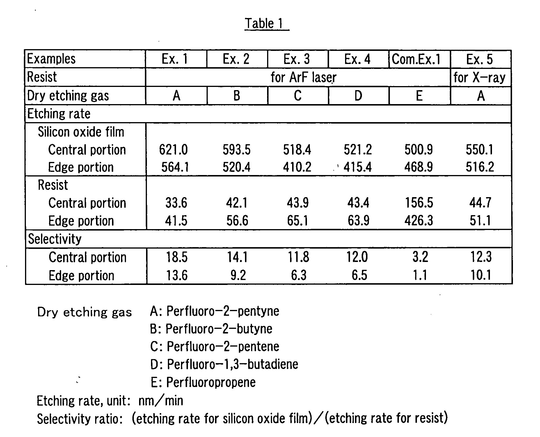
- the etching rate of the silicon oxide film was 621.0 nm/min at the central portion and 564.1 nm/min at the edge portion.
- the etching rate of the resist film was 33.6 nm/min at the central portion and 41.5 nm/min at the edge portion.
- the selectivity ratio in etching was 18.5 in the central portion and 13.6 at the edge portion.
- Etching was carried out by the same procedures as those adopted in Example 1 except that perfluoro-2-butyne produced in Production Example 2 was used as a dry etching gas with all other conditions remaining the same. Etching rate and selectivity ratio were evaluated in the same manner as in Example 1.
- Etching was carried out by the same procedures as those adopted in Example 1 except that perfluoro-2-pentene produced in Production Example 3 was used as a dry etching gas with all other conditions remaining the same. Etching rate and selectivity ratio were evaluated in the same manner as in Example 1.
- Etching was carried out by the same procedures as those adopted in Example 1 except that perfluoro-1,3-butadiene having a purity of 99.9% by volume, prepared by fractionating commercially available perfluoro-1,3-butadiene (available from SynQuest Laboratories, Inc.), was used as a dry etching gas with all other conditions remaining the same. Etching rate and selectivity ratio were evaluated in the same manner as in Example 1.
- Etching was carried out by the same procedures as those adopted in Example 1 except that perfluoropropene having a purity of 99.9% by volume, prepared by fractionating commercially available perfluoropropene (available from SynQuest Laboratories, Inc.), was used as a dry etching gas with all other conditions remaining the same. Etching rate and selectivity ratio were evaluated in the same manner as in Example 1. The results are shown in Table 1.
- a silicon substrate of an 8 inch diameter having a coating of silicon oxide film with a thickness of 2 ⁇ m was coated with the above-mentioned resist solution by a spin-coating procedure, and then, the thus-coated substrate was pre-baked at 120°C on a hot plate to form a resist film having a thickness of 300 nm.
- the resist film was exposed to light through a mask pattern by an X-ray aligner.
- the X-ray-exposed resist film was post-baked at 130°C, and then subjected to a developing treatment at 25°C for 60 seconds with an aqueous solution of tetramethylammonium hydroxide having a concentration of 2.38% by weight, and dried to form contact holes having a diameter of 100 nm.
- the thus-obtained substrate having contact holes was set in an ICP plasma etching apparatus.
- the inside of the apparatus was vacuumed, and perfluoro-2-pentyne as a dry etching gas, produced in Example 6, mentioned below, was introduced into the etching apparatus at a rate of 50 sccm.
- Etching was carried out at a plasma density of 10 11 ions/cm 3 while the inner pressure was maintained at 0.67 Pa. Etching rate and selectivity ratio were evaluated in the same manner as in Example 1.
- a round glass flask equipped with a cooling tube was charged with 140 parts of dimethylformamide.
- the flask was cooled to -50°C, and pentafluoropropionaldehyde was blown into the dimethylformamide to prepare a solution of pentafluoropropionaldehyde in dimethylformamide.
- the pentafluoropropionaldehyde used was prepared by heating 12.8 parts of pentafluoropropionaldehyde hydrate (available from Central Yakuhin K.K.) together with phosphorus(V) oxide whereby the pentafluoropropionaldehyde hydrate was dehydrated.
- the thus-obtained liquid extract was dried over sodium sulfate.
- the dried product was distilled to remove ether to give 36 parts of a crude product.
- GC-MS analysis of the crude product revealed that 2-chloro-1,1,1,4,4,5,5,5-octafluoro-2-pentene was produced.
- a Hastelloy autoclave was charged with 23.9 parts of commercially available palletized potassium hydroxide having a purity of 85% by weight and 36 parts of the above-mentioned 2-chloro-1,1,1,4,4,5,5,5-octafluoro-2-pentene. The content was thoroughly stirred and a reaction was carried out at 200°C for 6 hours.
- the autoclave was cooled, and the reaction mixture was distilled out.
- a trap for collection and a vacuum pump were connected, and the reaction mixture was collected at a subatmospheric pressure in the trap, cooled by liquid nitrogen, to give 3.7 parts of a reaction product.
- a high etching rate and a high etching selectivity can be attained and a fine resist pattern can be formed with good stability on a silicon substrate, even for a resist having poor resistance to dry etching using a light source with a short wavelength of 195 nm or less.
- the dry etching method of the present invention is beneficially adopted for the production of semiconductor devices having integrated circuits of high integration and high performance such as VLSI (very large scale integrated circuit) and ULSI (ultra large scale integrated circuit).
- perfluoro-2-pentyne having a high purity can be easily produced from a readily available raw material.
Landscapes
- Chemical & Material Sciences (AREA)
- Organic Chemistry (AREA)
- Chemical Kinetics & Catalysis (AREA)
- Drying Of Semiconductors (AREA)
- Organic Low-Molecular-Weight Compounds And Preparation Thereof (AREA)
- Addition Polymer Or Copolymer, Post-Treatments, Or Chemical Modifications (AREA)
Abstract
Description
→ CF3CX=CHCF2 CF3 + ZnX2 + ZnO
→ CF3C≡CCF2 CF3 + KX + H2O
Claims (12)
- A dry etching method characterized in that a resist film formed on a substrate is irradiated with radiation having a wavelength of not more than 195 nm to form a resist pattern having a minimum line width of not more than 200 nm, and the substrate having the resist pattern formed thereon is subjected to dry etching using a fluorine-containing compound having 4 to 6 carbon atoms and at least one unsaturated bond as an etching gas.
- The dry etching method according to claim 1, wherein the resist film is formed from a high molecular weight compound containing 0% to 10% by weight of repeating units having an aromatic ring structure.
- The dry etching method according to claim 1 or 2, wherein the fluorine-containing compound having 4 to 6 carbon atoms and at least one unsaturated bond is selected from perfuloro-2-butyne and perfuloro-2-pentyne.
- The dry etching method according to claim 1 or 2, wherein the fluorine-containing compound having 4 to 6 carbon atoms is perfuloro-2-pentyne.
- The dry etching method according to claim 1 or 2, wherein the fluorine-containing compound having 4 to 6 carbon atoms and at least one unsaturated bond is at least one kind of fluoropentene selected from 1,1,1,2,4,4,5,5,5-nonafluoro-2-pentene, 1,1,1,3,4,4,5-nonafluoro-2-pentene and perfluoro-2-pentene.
- The dry etching method according to any one of claims 1 to 5, wherein the dry etching is carried out under irradiation with plasma having a plasma density of at least 1010 ions/cm3.
- A dry etching gas comprised of a fluorine-containing compound having 4 to 6 carbon atoms and at least one unsaturated bond, and used for dry etching for a resist film forming a resist pattern having a minimum line width of not more than 200 nm at irradiation with radiation having a wavelength of not more than 195 nm.
- The dry etching gas according to claim 7, wherein the fluorine-containing compound having 4 to 6 carbon atoms and at least one unsaturated bond is selected from perfuloro-2-butyne and perfuloro-2-pentyne.
- The dry etching gas according to claim 7, wherein the fluorine-containing compound having 4 to 6 carbon atoms and at least one unsaturated bond is perfuloro-2-pentyne.
- The dry etching gas according to claim 7, wherein the fluorine-containing compound having 4 to 6 carbon atoms and at least one unsaturated bond is at least one kind of fluoropentene selected from 1,1,1,2,4,4,5,5,5-nonafluoro-2-pentene, 1,1,1,3,4,4,5-nonafluoro-2-pentene and perfluoro-2-pentene.
- A process for producing perfluoro-2-pentyne characterized in that a 1,1,1-trihalo-2,2,2-trifluoroethane is allowed to react with pentafluoropropionaldehyde to give a 2-halo-1,1,1,4,4,5,5,5-octafluoro-2-pentene, and the thus-produced 2-halo-1,1,1,4,4,5,5,5-octafluoro-2-pentene is dehydrohalogenated.
- The process for producing perfluoro-2-pentyne according to claim 11, wherein the 1,1,1-trihalo-2,2,2-trifluoroethane is 1,1,1-trichloro-2,2,2-trifluoroethane.
Applications Claiming Priority (3)
| Application Number | Priority Date | Filing Date | Title |
|---|---|---|---|
| JP2002208604 | 2002-07-17 | ||
| JP2002208604A JP4164643B2 (en) | 2002-07-17 | 2002-07-17 | Dry etching method and method for producing perfluoro-2-pentyne |
| PCT/JP2003/009023 WO2004008515A1 (en) | 2002-07-17 | 2003-07-16 | Method of dry etching, dry etching gas and process for producing perfluoro-2-pentyne |
Publications (2)
| Publication Number | Publication Date |
|---|---|
| EP1542268A1 true EP1542268A1 (en) | 2005-06-15 |
| EP1542268A4 EP1542268A4 (en) | 2007-01-31 |
Family
ID=30112852
Family Applications (1)
| Application Number | Title | Priority Date | Filing Date |
|---|---|---|---|
| EP03764209A Withdrawn EP1542268A4 (en) | 2002-07-17 | 2003-07-16 | DRY ETCHING METHOD, DRY ETCHING GAS AND PROCESS FOR PRODUCING PERFLUORO-2-PENTYNE |
Country Status (7)
| Country | Link |
|---|---|
| US (1) | US20050247670A1 (en) |
| EP (1) | EP1542268A4 (en) |
| JP (1) | JP4164643B2 (en) |
| KR (1) | KR101001128B1 (en) |
| CN (1) | CN100359644C (en) |
| TW (1) | TWI288442B (en) |
| WO (1) | WO2004008515A1 (en) |
Families Citing this family (15)
| Publication number | Priority date | Publication date | Assignee | Title |
|---|---|---|---|---|
| US7341764B2 (en) * | 2001-11-08 | 2008-03-11 | Zeon Corporation | Gas for plasma reaction, process for producing the same, and use |
| JPWO2005117082A1 (en) * | 2004-05-31 | 2008-04-03 | 独立行政法人産業技術総合研究所 | Dry etching gas and dry etching method |
| JP4853063B2 (en) | 2006-03-15 | 2012-01-11 | オムロン株式会社 | User device, communication device, authentication system, authentication method, authentication program, and recording medium |
| WO2007114359A1 (en) * | 2006-03-31 | 2007-10-11 | Zeon Corporation | Process for production of perfluoroalkine compound |
| TW200834662A (en) * | 2006-12-12 | 2008-08-16 | Applied Materials Inc | Wet photoresist stripping process and apparatus |
| US20080191163A1 (en) * | 2007-02-09 | 2008-08-14 | Mocella Michael T | Laser-Assisted Etching Using Gas Compositions Comprising Unsaturated Fluorocarbons |
| JP5440170B2 (en) * | 2007-09-28 | 2014-03-12 | 日本ゼオン株式会社 | Plasma etching method |
| US20110136345A1 (en) * | 2008-07-15 | 2011-06-09 | Solvay Fluor Gmbh | Process for the Manufacture of Etched Items |
| JP2010100592A (en) * | 2008-10-27 | 2010-05-06 | National Institute Of Advanced Industrial Science & Technology | Method for producing fluorine-containing compound |
| CN102741987B (en) * | 2010-02-01 | 2016-03-02 | 中央硝子株式会社 | Dry ecthing agent and use its dry-etching method |
| SG11201605356PA (en) * | 2013-12-30 | 2016-07-28 | Chemours Co Fc Llc | Chamber cleaning and semiconductor etching gases |
| US9252051B1 (en) | 2014-11-13 | 2016-02-02 | International Business Machines Corporation | Method for top oxide rounding with protection of patterned features |
| US9934984B2 (en) | 2015-09-09 | 2018-04-03 | International Business Machines Corporation | Hydrofluorocarbon gas-assisted plasma etch for interconnect fabrication |
| JP7436777B2 (en) * | 2019-07-12 | 2024-02-22 | ダイキン工業株式会社 | Method for producing fluoroolefin compounds |
| JP7343796B2 (en) * | 2021-04-27 | 2023-09-13 | ダイキン工業株式会社 | Method for producing fluoroalkyne compounds |
Family Cites Families (24)
| Publication number | Priority date | Publication date | Assignee | Title |
|---|---|---|---|---|
| US3291844A (en) * | 1963-10-10 | 1966-12-13 | Dow Chemical Co | Catalytic preparation of fluoroethers |
| US4745042A (en) * | 1984-04-19 | 1988-05-17 | Matsushita Electric Industrial Co., Ltd. | Water-soluble photopolymer and method of forming pattern by use of the same |
| US4621126A (en) * | 1984-06-08 | 1986-11-04 | E. I. Du Pont De Nemours And Company | Group transfer polymerization employing tris(disubstituted amino)sulfonium perfluorocarbanion salts as catalysts |
| US5556501A (en) * | 1989-10-03 | 1996-09-17 | Applied Materials, Inc. | Silicon scavenger in an inductively coupled RF plasma reactor |
| JP3008510B2 (en) * | 1991-02-16 | 2000-02-14 | ダイキン工業株式会社 | Method for producing dimer of fluorinated ethane |
| US6171974B1 (en) * | 1991-06-27 | 2001-01-09 | Applied Materials, Inc. | High selectivity oxide etch process for integrated circuit structures |
| JPH07278029A (en) * | 1994-04-13 | 1995-10-24 | Daikin Ind Ltd | Azeotropic composition |
| JPH09191002A (en) * | 1996-01-10 | 1997-07-22 | Sony Corp | Plasma etching method |
| US6270948B1 (en) * | 1996-08-22 | 2001-08-07 | Kabushiki Kaisha Toshiba | Method of forming pattern |
| US6031141A (en) * | 1997-08-25 | 2000-02-29 | E. I. Du Pont De Nemours And Company | Fluoroolefin manufacturing process |
| US6387287B1 (en) * | 1998-03-27 | 2002-05-14 | Applied Materials, Inc. | Process for etching oxide using a hexafluorobutadiene and manifesting a wide process window |
| JP2000007593A (en) * | 1998-06-24 | 2000-01-11 | Asahi Glass Co Ltd | Method for producing perfluoro (n-pentane) |
| US6147267A (en) * | 1998-11-10 | 2000-11-14 | E. I. Du Pont De Nemours And Company | Process for perfluorocycloalkane purification |
| JP2000206704A (en) * | 1999-01-14 | 2000-07-28 | Toshiba Corp | Pattern formation method |
| JP2000349152A (en) * | 1999-03-29 | 2000-12-15 | Sony Corp | Method for manufacturing semiconductor device |
| JP3375605B2 (en) * | 1999-08-02 | 2003-02-10 | 松下電器産業株式会社 | Plasma processing method |
| US6362109B1 (en) * | 2000-06-02 | 2002-03-26 | Applied Materials, Inc. | Oxide/nitride etching having high selectivity to photoresist |
| KR100379976B1 (en) * | 2000-11-27 | 2003-04-16 | 삼성전자주식회사 | Etching gas composition of silicone oxides and method of etching silicone oxides using the same |
| WO2002050885A1 (en) * | 2000-12-21 | 2002-06-27 | Tokyo Electron Limited | Etching method for insulating film |
| US6897120B2 (en) * | 2001-01-03 | 2005-05-24 | Micron Technology, Inc. | Method of forming integrated circuitry and method of forming shallow trench isolation in a semiconductor substrate |
| US6664431B2 (en) * | 2001-03-14 | 2003-12-16 | Zakrytoe Aktsionernoe Obschestvo Nauchno-Proizvodstvennoe Obiedinenie “Pim-Invest” | Process for producing fluorinated aliphatic compounds |
| JP4418605B2 (en) * | 2001-04-11 | 2010-02-17 | パナソニック株式会社 | Pattern forming material and pattern forming method |
| US7341764B2 (en) * | 2001-11-08 | 2008-03-11 | Zeon Corporation | Gas for plasma reaction, process for producing the same, and use |
| JP2003282540A (en) * | 2002-03-25 | 2003-10-03 | Tokyo Electron Ltd | Plasma etching method |
-
2002
- 2002-07-17 JP JP2002208604A patent/JP4164643B2/en not_active Expired - Fee Related
-
2003
- 2003-07-16 TW TW092119395A patent/TWI288442B/en not_active IP Right Cessation
- 2003-07-16 CN CNB03816972XA patent/CN100359644C/en not_active Expired - Fee Related
- 2003-07-16 US US10/520,272 patent/US20050247670A1/en not_active Abandoned
- 2003-07-16 EP EP03764209A patent/EP1542268A4/en not_active Withdrawn
- 2003-07-16 KR KR1020057000709A patent/KR101001128B1/en not_active Expired - Fee Related
- 2003-07-16 WO PCT/JP2003/009023 patent/WO2004008515A1/en not_active Ceased
Also Published As
| Publication number | Publication date |
|---|---|
| KR20050025601A (en) | 2005-03-14 |
| TWI288442B (en) | 2007-10-11 |
| EP1542268A4 (en) | 2007-01-31 |
| US20050247670A1 (en) | 2005-11-10 |
| WO2004008515A1 (en) | 2004-01-22 |
| CN1669129A (en) | 2005-09-14 |
| CN100359644C (en) | 2008-01-02 |
| TW200405461A (en) | 2004-04-01 |
| JP2004055680A (en) | 2004-02-19 |
| KR101001128B1 (en) | 2010-12-14 |
| JP4164643B2 (en) | 2008-10-15 |
Similar Documents
| Publication | Publication Date | Title |
|---|---|---|
| US20050247670A1 (en) | Method of dry etching, dry etching gas and process for producing perfluoro-2-pentyne | |
| US8535551B2 (en) | Plasma etching method | |
| JP4978512B2 (en) | Plasma etching method | |
| JP5131436B2 (en) | Etching method | |
| US9368363B2 (en) | Etching gas and etching method | |
| US7652179B2 (en) | Gas for plasma reaction, process for producing the same, and use thereof | |
| JP2003238620A (en) | Fluorine-containing polymerizable monomer and polymer compound, anti-reflection coating material and resist material using the polymer | |
| WO2021145343A1 (en) | Copolymer, positive resist composition, and method for forming resist pattern | |
| JP2009206394A (en) | Forming method of carbon-based hard mask | |
| WO2006011427A1 (en) | Fluorine-containing compound, fluorine-containing polymer, resist composition and resist protective film composition | |
| JPWO2005117082A1 (en) | Dry etching gas and dry etching method | |
| JP2008081477A (en) | Oxygen-containing fluorine compound container filling, oxygen-containing fluorine compound storage method, and plasma etching method | |
| CN101015044A (en) | Dry etching gases and method of dry etching | |
| TW201103972A (en) | Process for the manufacture of etched items | |
| US7163982B2 (en) | Process for preparing fluorine-containing polymer and method of forming fine pattern using same | |
| WO2004024787A1 (en) | Process for production of fluoropolymers for resist | |
| EP1559729A1 (en) | Fluoropolymer | |
| JP2005234520A (en) | Method for producing fluoropolymer and method for forming fine pattern using the same | |
| KR20070018964A (en) | Dry etching gas and dry etching method |
Legal Events
| Date | Code | Title | Description |
|---|---|---|---|
| PUAI | Public reference made under article 153(3) epc to a published international application that has entered the european phase |
Free format text: ORIGINAL CODE: 0009012 |
|
| 17P | Request for examination filed |
Effective date: 20050119 |
|
| AK | Designated contracting states |
Kind code of ref document: A1 Designated state(s): AT BE BG CH CY CZ DE DK EE ES FI FR GB GR HU IE IT LI LU MC NL PT RO SE SI SK TR |
|
| RBV | Designated contracting states (corrected) |
Designated state(s): DE FR GB IE IT |
|
| RIC1 | Information provided on ipc code assigned before grant |
Ipc: H01L 21/311 20060101AFI20061219BHEP Ipc: C07C 21/22 20060101ALI20061219BHEP Ipc: H01L 21/3213 20060101ALI20061219BHEP |
|
| A4 | Supplementary search report drawn up and despatched |
Effective date: 20070102 |
|
| 17Q | First examination report despatched |
Effective date: 20070613 |
|
| GRAP | Despatch of communication of intention to grant a patent |
Free format text: ORIGINAL CODE: EPIDOSNIGR1 |
|
| RIC1 | Information provided on ipc code assigned before grant |
Ipc: H01L 21/3213 20060101ALI20140707BHEP Ipc: C07C 17/25 20060101ALI20140707BHEP Ipc: C07C 17/263 20060101ALI20140707BHEP Ipc: C07C 21/22 20060101ALI20140707BHEP Ipc: C07C 21/18 20060101ALI20140707BHEP Ipc: H01L 21/311 20060101AFI20140707BHEP |
|
| INTG | Intention to grant announced |
Effective date: 20140730 |
|
| STAA | Information on the status of an ep patent application or granted ep patent |
Free format text: STATUS: THE APPLICATION IS DEEMED TO BE WITHDRAWN |
|
| 18D | Application deemed to be withdrawn |
Effective date: 20141210 |