EP1542264A1 - Cvd apparatus having means for cleaning with fluorine gas and method of cleaning cvd apparatus with fluorine gas - Google Patents
Cvd apparatus having means for cleaning with fluorine gas and method of cleaning cvd apparatus with fluorine gas Download PDFInfo
- Publication number
- EP1542264A1 EP1542264A1 EP03712689A EP03712689A EP1542264A1 EP 1542264 A1 EP1542264 A1 EP 1542264A1 EP 03712689 A EP03712689 A EP 03712689A EP 03712689 A EP03712689 A EP 03712689A EP 1542264 A1 EP1542264 A1 EP 1542264A1
- Authority
- EP
- European Patent Office
- Prior art keywords
- fluorine
- fluorine gas
- cvd apparatus
- component
- cleaning
- Prior art date
- Legal status (The legal status is an assumption and is not a legal conclusion. Google has not performed a legal analysis and makes no representation as to the accuracy of the status listed.)
- Withdrawn
Links
Images




Classifications
-
- B—PERFORMING OPERATIONS; TRANSPORTING
- B08—CLEANING
- B08B—CLEANING IN GENERAL; PREVENTION OF FOULING IN GENERAL
- B08B7/00—Cleaning by methods not provided for in a single other subclass or a single group in this subclass
- B08B7/0035—Cleaning by methods not provided for in a single other subclass or a single group in this subclass by radiant energy, e.g. UV, laser, light beam or the like
-
- C—CHEMISTRY; METALLURGY
- C23—COATING METALLIC MATERIAL; COATING MATERIAL WITH METALLIC MATERIAL; CHEMICAL SURFACE TREATMENT; DIFFUSION TREATMENT OF METALLIC MATERIAL; COATING BY VACUUM EVAPORATION, BY SPUTTERING, BY ION IMPLANTATION OR BY CHEMICAL VAPOUR DEPOSITION, IN GENERAL; INHIBITING CORROSION OF METALLIC MATERIAL OR INCRUSTATION IN GENERAL
- C23C—COATING METALLIC MATERIAL; COATING MATERIAL WITH METALLIC MATERIAL; SURFACE TREATMENT OF METALLIC MATERIAL BY DIFFUSION INTO THE SURFACE, BY CHEMICAL CONVERSION OR SUBSTITUTION; COATING BY VACUUM EVAPORATION, BY SPUTTERING, BY ION IMPLANTATION OR BY CHEMICAL VAPOUR DEPOSITION, IN GENERAL
- C23C16/00—Chemical coating by decomposition of gaseous compounds, without leaving reaction products of surface material in the coating, i.e. chemical vapour deposition [CVD] processes
- C23C16/44—Chemical coating by decomposition of gaseous compounds, without leaving reaction products of surface material in the coating, i.e. chemical vapour deposition [CVD] processes characterised by the method of coating
- C23C16/4401—Means for minimising impurities, e.g. dust, moisture or residual gas, in the reaction chamber
- C23C16/4405—Cleaning of reactor or parts inside the reactor by using reactive gases
-
- H—ELECTRICITY
- H01—ELECTRIC ELEMENTS
- H01J—ELECTRIC DISCHARGE TUBES OR DISCHARGE LAMPS
- H01J37/00—Discharge tubes with provision for introducing objects or material to be exposed to the discharge, e.g. for the purpose of examination or processing thereof
- H01J37/32—Gas-filled discharge tubes
- H01J37/32009—Arrangements for generation of plasma specially adapted for examination or treatment of objects, e.g. plasma sources
- H01J37/32357—Generation remote from the workpiece, e.g. down-stream
-
- H—ELECTRICITY
- H01—ELECTRIC ELEMENTS
- H01J—ELECTRIC DISCHARGE TUBES OR DISCHARGE LAMPS
- H01J37/00—Discharge tubes with provision for introducing objects or material to be exposed to the discharge, e.g. for the purpose of examination or processing thereof
- H01J37/32—Gas-filled discharge tubes
- H01J37/32431—Constructional details of the reactor
- H01J37/32798—Further details of plasma apparatus not provided for in groups H01J37/3244 - H01J37/32788; special provisions for cleaning or maintenance of the apparatus
- H01J37/32853—Hygiene
- H01J37/32862—In situ cleaning of vessels and/or internal parts
-
- Y—GENERAL TAGGING OF NEW TECHNOLOGICAL DEVELOPMENTS; GENERAL TAGGING OF CROSS-SECTIONAL TECHNOLOGIES SPANNING OVER SEVERAL SECTIONS OF THE IPC; TECHNICAL SUBJECTS COVERED BY FORMER USPC CROSS-REFERENCE ART COLLECTIONS [XRACs] AND DIGESTS
- Y02—TECHNOLOGIES OR APPLICATIONS FOR MITIGATION OR ADAPTATION AGAINST CLIMATE CHANGE
- Y02C—CAPTURE, STORAGE, SEQUESTRATION OR DISPOSAL OF GREENHOUSE GASES [GHG]
- Y02C20/00—Capture or disposal of greenhouse gases
- Y02C20/30—Capture or disposal of greenhouse gases of perfluorocarbons [PFC], hydrofluorocarbons [HFC] or sulfur hexafluoride [SF6]
-
- Y—GENERAL TAGGING OF NEW TECHNOLOGICAL DEVELOPMENTS; GENERAL TAGGING OF CROSS-SECTIONAL TECHNOLOGIES SPANNING OVER SEVERAL SECTIONS OF THE IPC; TECHNICAL SUBJECTS COVERED BY FORMER USPC CROSS-REFERENCE ART COLLECTIONS [XRACs] AND DIGESTS
- Y02—TECHNOLOGIES OR APPLICATIONS FOR MITIGATION OR ADAPTATION AGAINST CLIMATE CHANGE
- Y02P—CLIMATE CHANGE MITIGATION TECHNOLOGIES IN THE PRODUCTION OR PROCESSING OF GOODS
- Y02P70/00—Climate change mitigation technologies in the production process for final industrial or consumer products
- Y02P70/50—Manufacturing or production processes characterised by the final manufactured product
Definitions
- the present invention relates to a chemical vapor deposition (CVD) apparatus for forming a uniform thin film of high quality, for example, silicon oxide (SiO 2 ) or silicon nitride (Si 3 N 4 or the like) on a surface of a base material for a semiconductor such as a silicon wafer.
- CVD chemical vapor deposition
- the present invention relates to a CVD apparatus capable of executing cleaning for removing a by-product adhered to an inner wall of a reaction chamber or the like after a thin film forming process, and a method of cleaning the CVD apparatus using the same.
- a thin film such as silicon oxide (SiO 2 ) or silicon nitride (Si 3 N 4 or the like) is widely used in a semiconductor element such as a thin film transistor, a photoelectric converting element or the like.
- a semiconductor element such as a thin film transistor, a photoelectric converting element or the like.
- the following three kinds of techniques for forming a thin film such as silicon oxide, silicon nitride or the like are mainly used.
- the plasma CVD technique plasma enhanced chemical vapor deposition in (3) is widely used because a minute and uniform thin film can efficiently be formed.
- a plasma CVD apparatus 100 to be used in the plasma CVD technique is generally constituted as shown in Fig. 7.
- the plasma CVD apparatus 100 comprises a reaction chamber 102 maintained in a decompression state, and an upper electrode 104 and a lower electrode 106 are provided to be opposed apart from each other at a constant interval in the reaction chamber 102.
- a film forming gas supply path 108 connected to a film forming gas source (not shown) is connected to the upper electrode 104, and a film forming gas is supplied into the reaction chamber 102 through the upper electrode 104.
- a high frequency applicator 110 for applying a high frequency is connected to the reaction chamber 102 in the vicinity of the upper electrode 104. Furthermore, an exhaust path 114 for exhausting a gas through a pump 112 is connected to the reaction chamber 102.
- the plasma CVD apparatus 100 thus constituted, for example, monosilane (SiH 4 ), N 2 O, N 2 , O 2 , Ar or the like in the formation of the film of silicon oxide (SiO 2 ) and the monosilane (SiH 4 ), NH 3 , N 2 , O 2 , Ar or the like in the formation of the film of silicon nitride (Si 3 N 4 or the like) are introduced through the film forming gas supply path 108 and the upper electrode 104 into the reaction chamber 102 which is maintained in a decompression state of 130 Pa, for example.
- a high frequency power of 13.56 MHz is applied between the electrodes 104 and 106, which are provided opposite to each other in the reaction chamber 102, through the high frequency applicator 110, for example.
- a high frequency electric field is generated, electrons are impacted with neutral molecules of a film forming gas in the electric field, and a high frequency plasma is formed so that the film forming gas is dissociated into ions and radicals.
- a silicon thin film is formed on a surface of a semiconductor product W such as a silicon wafer which is provided on one of the electrodes (the lower electrode 106).
- a thin film material such as SiO 2 or Si 3 N 4 is also adhered to and deposited on the surfaces of an inner wall, an electrode and the like in the reaction chamber 102 other than the semiconductor product W to be formed by a discharge in the reaction chamber 102 so that a by-product is obtained.
- this by-product grows to have a constant thickness, it is peeled by a dead weight, a stress or the like.
- fine particles to be foreign matters are mixed into the semiconductor product so that contamination is caused. For this reason, a thin film of high quality cannot be manufactured so that the disconnection or short-circuit of a semiconductor circuit is caused.
- a yield or the like might be deteriorated.
- a by-product is removed by using, for example, a cleaning gas obtained by adding a fluorocompound such as CF 4 , C 2 F 6 or COF 2 , and O 2 or the like if necessary in order to remove such a by-product at any time after the film forming step is ended in the plasma CVD apparatus 100.
- a cleaning gas obtained by adding a fluorocompound such as CF 4 , C 2 F 6 or COF 2 , and O 2 or the like if necessary in order to remove such a by-product at any time after the film forming step is ended in the plasma CVD apparatus 100.
- a cleaning gas containing a fluorocompound such as the CF 4 , the C 2 F 6 or the COF 2 is accompanied by a gas such as O 2 and/or Ar in place of a film forming gas in the film formation.
- the cleaning gas is introduced into the reaction chamber 102, which is maintained in a decompression state, through the film forming gas supply path 108 and the upper electrode 104.
- a high frequency power is applied between the electrodes 104 and 106, which are provided opposite to each other in the reaction chamber 102, through the high frequency applicator 110.
- a high frequency electric field is generated, electrons are impacted with the neutral molecules of the cleaning gas in the electric field, and a high frequency plasma is formed so that the cleaning gas is dissociated into ions and radicals.
- the ions and the radicals react to a by-product such as SiO 2 or Si 3 N 4 which is adhered to and deposited on the surfaces of an inner wall, an electrode and the like in the reaction chamber 102.
- the by-product is gasified as SiF 4 and is discharged from the pump 112 to the outside of the reaction chamber 102 through the exhaust path 114 together with an exhaust gas.
- the fluorocompound such as CF 4 or C 2 F 6 to be used as the cleaning gas is a stable compound having a long life in the atmospheric air. Furthermore, there is a problem in that a gas discharging process is hard to perform after the cleaning and a disposal cost is increased. Moreover, global warming factors (values for a cumulative period of 100 years) of CF 4 , C 2 F 6 and SF 6 are 6500, 9200 and 23900 respectively, and they are extremely large. Therefore, an adverse influence thereof on an environment is apprehended.
- the ratio of a gas discharged to the outside of the reaction chamber 102 through the exhaust path 114 is high, that is, approximately 60% in case of C 2 F 6 , for example. Therefore, it has an adverse influence on global warming, and a dissociation efficiency is low and a cleaning capability is also low.
- an added gas such as oxygen or argon is usually mixed in a proper amount and is thus used together with a cleaning gas.
- a mixed gas type of the cleaning gas and the added gas when the content concentration of the cleaning gas is increased under the condition that a total gas flow is constant, an etching speed tends to be increased. If the concentration of the cleaning gas is more than a certain concentration, however, there is a problem in that the generation of a plasma becomes unstable, the etching speed is decreased or a cleaning uniformity is deteriorated. If the cleaning gas is used in a concentration of 100%, particularly, there is a problem in that the instability of the generation of the plasma, the decrease in the etching speed and the deterioration in the cleaning uniformity tend to be more remarkable so that a utility cannot be obtained.
- the cleaning gas is to be diluted for use in such a manner that a concentration thereof is reduced to be equal to or lower than the peak concentration of an etching speed and cleaning gas concentration curve.
- cleaning conditions are optimized by raising a chamber pressure or increasing a gas flow in the cleaning. If the chamber pressure is raised or the gas flow is increased in the cleaning, however, the generation of a plasma becomes unstable and the cleaning uniformity is deteriorated so that the cleaning cannot be efficiently carried out.
- a fluorine gas rarely influences the environment and a plasma can be stably generated under the condition that a total gas flow is approximately 1000 sccm and a chamber pressure is approximately 400 Pa by using the fluorine gas as a cleaning gas.
- a plasma processing can be carried out, a very excellent etching speed can be obtained, and furthermore, an excellent cleaning uniformity can be maintained.
- an F atom generated by the plasma has a stability and a gas discharged by using the fluorine gas as a cleaning gas is the fluorine gas, and the cleaning process can be efficiently carried out by using the fluorine gas in a necessary amount as the cleaning gas.
- the conventional fluorine gas generating device for generating a fluorine gas has such a structure that KF is dissolved as an electrolyte in an HF anhydride solution and an electrolyte is electrolyzed by a carbon electrode to obtain the fluorine gas.
- Such a conventional fluorine gas generating device is large-sized and cannot be used safely. Therefore, it is necessary for a special safety administrator to carry out maintenance. If the fluorine gas generating device is used in a CVD apparatus, the size of the CVD apparatus is increased, and furthermore, a complicated work is required for maintenance and control.
- the cleaning gas is required in an amount of 750 sccm per wafer for one minute.
- the fluorine gas is required in an amount of 100 moles, that is, 3.8 kg. If this amount is converted into a 29 atm filled 47L cylinder, two cylinders are required for one reaction chamber.
- a fluorine gas cylinder is provided in the CVD apparatus in place of the conventional fluorine gas generating device, accordingly, the size of the apparatus is increased, and furthermore, the exchange of the cylinder is complicated, which is inconvenient.
- the present invention is to provide a CVD apparatus capable of executing cleaning in which a by-product such as SiO 2 or Si 3 N 4 , which is adhered to and deposited on the surfaces of an inner wall, an electrode and the like in a reaction chamber, can efficiently be removed at a film forming step. Furthermore, the present invention is to provide a CVD apparatus in which the amount of a cleaning gas to be discharged is very small, the influence on an environment such as global warming is also lessened, a gas utilization efficiency is also high and a cost can also be reduced and of manufacturing a thin film of high quality, and having a small-sized cleaning mechanism. In addition, the present invention is to provide a method of cleaning the CVD apparatus using the CVD apparatus.
- the present invention has been made in order to solve the problems and to attain the object in the prior art described above, and the present invention provides a CVD apparatus having a cleaning mechanism for supplying a reactive gas into a reaction chamber and forming a deposited film on a surface of a base material provided in the reaction chamber, comprising a fluorine gas generating device including:
- the energy is simply applied to react the fluorine compound so that the fluorine gas component and the component other than the fluorine gas component are generated and separated. Consequently, the fluorine gas component is separated and refined so that the fluorine gas can easily be obtained.
- the fluorine gas thus obtained is then converted to a plasma.
- the plasma By using the plasma to remove a by-product adhered into the reaction chamber, it is possible to obtain a very excellent etching speed. Thus, an excellent cleaning uniformity can be maintained.
- such a fluorine gas generating device has a smaller size as compared with a conventional fluorine gas generating device using electrolysis, and furthermore, the fluorine gas can be obtained efficiently.
- the CVD apparatus itself is also small-sized and maintenance can easily be carried out.
- the present invention provides the CVD apparatus having a cleaning mechanism, wherein the energy applying device is constituted to heat the fluorine compound, thereby reacting the fluorine compound to generate the fluorine gas component and the component other than the fluorine gas component.
- the present invention provides the method of cleaning a CVD apparatus, wherein the fluorine compound is heated and is thus reacted, thereby generating the fluorine gas component and the component other than the fluorine gas component.
- the present invention provides the CVD apparatus having a cleaning mechanism, wherein the energy applying device is constituted to apply a plasma to the fluorine compound, thereby reacting the fluorine compound to generate the fluorine gas component and the component other than the fluorine gas component.
- the present invention provides the method of cleaning a CVD apparatus, wherein a plasma is applied to the fluorine compound, thereby reacting the fluorine compound to generate the fluorine gas component and the component other than the fluorine gas component.
- the fluorine compound By simply applying a plasma to the fluorine compound, thus, the fluorine compound is reacted to generate the fluorine gas component and the component other than the fluorine gas component. Consequently, the fluorine gas component can be obtained. Therefore, a size can be more reduced as compared with a conventional fluorine gas generating device using electrolysis, and furthermore, the fluorine gas can be obtained efficiently.
- the CVD apparatus itself is also small-sized and the maintenance can easily be carried out.
- the present invention provides the CVD apparatus having a cleaning mechanism, wherein the energy applying device is constituted to react the fluorine compound by a catalyst, thereby generating the fluorine gas component and the component other than the fluorine gas component.
- the present invention provides the method of cleaning a CVD apparatus, wherein the fluorine compound is reacted by a catalyst, thereby generating the fluorine gas component and the component other than the fluorine gas component.
- the fluorine gas component and the component other than the fluorine gas component are generated so that the fluorine gas component can be obtained. Therefore, a size can be more reduced as compared with a conventional fluorine gas generating device using electrolysis, and furthermore, the fluorine gas can be obtained efficiently.
- the CVD apparatus itself is also small-sized and the maintenance can easily be carried out.
- the present invention provides the CVD apparatus having a cleaning mechanism, wherein the fluorine gas concentration/separation refining device is constituted to separate the fluorine gas component from the component other than the fluorine gas component by utilizing a difference in a boiling point which is made by cooling.
- the present invention provides the method of cleaning a CVD apparatus, wherein the fluorine gas component is separated from the component other than the fluorine gas component by utilizing a difference in a boiling point which is made by cooling.
- the fluorine gas component is separated from the component other than the fluorine gas component by utilizing the difference in the boiling point through cooling, trapping using liquid nitrogen, electron cooling or the like, for example. Therefore, a size can be more reduced as compared with a conventional fluorine gas generating device using electrolysis, and furthermore, the fluorine gas can be obtained efficiently.
- the CVD apparatus itself is also small-sized and the maintenance can easily be carried out.
- the present invention is characterized in that the fluorine compound contains nitrogen.
- examples of the fluorine compound containing the nitrogen include FNO and F 3 NO.
- the FNO is a stable substance. By using the FNO as a fluorine gas source, it is possible to utilize the fluorine gas as a cleaning gas more stably.
- the present invention is characterized in that the fluorine compound contains chlorine.
- the present invention is characterized in that the fluorine compound contains iodine.
- the fluorine compound contains the iodine, for example, such fluorine compound is IF 5 or IF 7 .
- a product such as IF 3 has a different boiling point from that of F 2 . Therefore, it is possible to easily separate the fluorine gas by using a refrigerant such as liquid nitrogen, dry ice or the like, for example.
- the present invention is characterized in that the fluorine compound contains sulfur.
- the fluorine compound contains the sulfur, for example, such fluorine compound is SF 6 .
- the boiling point of SO 2 F 2 is -83.1°C,that of SO 2 is -10°C and that of F 2 is -188.1°C, which are different from each other.
- the present invention is characterized in that the fluorine compound contains carbon.
- Fig. 1 is a schematic view showing a first example of a CVD apparatus having a cleaning mechanism according to the present invention.
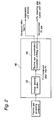
- Fig. 2 is a schematic view showing a cleaning gas generating device 40 in Fig. 1,
- Fig. 3 is a schematic view showing a second example of the CVD apparatus having the cleaning mechanism according to the present invention.
- Fig. 4 is the same schematic view as Fig. 2 showing the first example of the CVD apparatus having the cleaning mechanism according to the present invention.
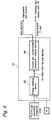
- Fig. 5 is the same schematic view as Fig. 2 showing the second example of the CVD apparatus having the cleaning mechanism according to the present invention.
- Fig. 6 is the same schematic view as Fig. 2 showing a third example of the CVD apparatus having the cleaning mechanism according to the present invention.
- Fig. 7 is a schematic view showing a plasma CVD apparatus to be used for a conventional plasma CVD method.
- Fig. 1 is a schematic view showing a first example of a CVD apparatus having a cleaning mechanism according to the present invention.
- a CVD apparatus 10 comprises a reaction chamber 12 maintained in a decompression state (a vacuum state).
- the reaction chamber 12 is maintained in a constant vacuum state (a decompression state) by discharging an internal gas to the outside through an exhaust path 16 formed on a bottom wall 12c of the reaction chamber 12, by means of a mechanical booster pump 11, a dry pump 14 and a toxicity removing device 13 for causing an exhaust gas to be nontoxic.
- a lower electrode 18 constituting a stage for mounting a base material A to deposit (vapor deposit or the like) a silicon thin film on a surface of a silicon wafer or the like, for example, is provided in the reaction chamber 12.
- the lower electrode 18 penetrates through the bottom wall 12c of the reaction chamber 12 and is constituted vertically slidably by a driving mechanism which is not shown, and a position can be adjusted.
- a sliding portion between the lower electrode 18 and the bottom wall 12c is provided with a seal member such as a seal ring in order to maintain a degree of vacuum in the reaction chamber 12, which is not shown.
- an upper electrode 20 is provided in the upper part of the reaction chamber 12. Furthermore, the upper electrode 20 has a base end portion 22 thereof which penetrates through a top wall 12a of the reaction chamber 12 and is connected to a high frequency power source 24 provided on the outside of the reaction chamber 12.
- the upper electrode 20 is provided with a high frequency applicator 25 such as a high frequency application coil which is not shown.
- a matching circuit (not shown) is provided between the high frequency applicator 25 and the high frequency power source 24. Consequently, it is possible to propagate a high frequency generated by the high frequency power source 24 to the high frequency applicator 25 such as the high frequency application coil without a loss.
- a reactive gas supply path 26 is formed on the upper electrode 20.
- a film forming gas is introduced from a film forming gas supply source 28 into the reaction chamber 12, which is maintained in a decompression state, through the reactive gas supply path 26 and the upper electrode 20.
- a cleaning gas supply path 30 is branched and connected to the reactive gas supply path 26.
- a cleaning gas can be introduced from a cleaning gas generating device 40 into the reaction chamber 12 through the cleaning gas supply path 30.
- the CVD apparatus 10 according to the present invention having such a structure is operated in the following manner.
- the base material A for depositing a silicon thin film on a surface of a silicon wafer or the like, for example, is mounted over the stage of the lower electrode 18 in the reaction chamber 12. Thereafter, a distance from the upper electrode 20 is regulated to be a predetermined distance by a driving mechanism which is not shown.
- An internal gas is discharged to the outside through the dry pump 14 via the exhaust path 16 formed on the bottom wall 12c in the reaction chamber 12. Consequently, a constant vacuum state (a decompression state), for example, a decompression state of 10 to 2000 Pa is maintained.
- a decompression state for example, a decompression state of 10 to 2000 Pa is maintained.
- a switching valve 52 provided on the reactive gas supply path 26 is opened and a film forming gas is introduced from the film forming gas supply source 28 into the reaction chamber 12, which is maintained in the decompression state, through the reactive gas supply path 26 and the upper electrode 20.
- the switching valve 52 provided on the reactive gas supply path 26 and a switching valve 54 provided on the exhaust path 16 are opened.
- a switching valve 56 provided on the cleaning gas supply path 30 is closed.
- monosilane (SiH 4 ), N 2 O, N 2 , O 2 , Ar and the like in the formation of the film of silicon oxide (SiO 2 ) and the monosilane (SiH 4 ), NH 3 , N 2 , O 2 and Ar in the formation of the film of silicon nitride (Si 3 N 4 or the like) should be supplied as the film forming gas which is to be supplied from the film forming gas supply source 28, for example.
- the film forming gas is not restricted to them but they can properly be changed, for example, disilane (Si 2 H 6 ), TEOS (tetraethoxysilane ; Si(OC 2 H 5 ) 4 ) or the like is used as the film forming gas and O 2 , O 3 or the like is used as a carrier gas depending on the type of a thin film to be formed, for example.
- disilane Si 2 H 6
- TEOS tetraethoxysilane ; Si(OC 2 H 5 ) 4
- O 2 , O 3 or the like is used as a carrier gas depending on the type of a thin film to be formed, for example.
- a high frequency electric field is generated from the high frequency applicator 25 such as a high frequency application coil to the upper electrode 20 by a high frequency generated from the high frequency power source 24. Then, electrons are impacted with neutral molecules of the film forming gas in the electric field. As a result, a high frequency plasma is formed and the film forming gas is dissociated into ions and radicals. By the actions of the ions and radicals, a silicon thin film is formed on the surface of the base material A such as a silicon wafer which is provided on the lower electrode 18.
- a thin film material such as SiO 2 or Si 3 N 4 is also adhered to and deposited on the surfaces of an inner wall, an electrode and the like in the reaction chamber 12 other than a semiconductor product A to be formed.
- a by-product is obtained by a discharge in the reaction chamber 12.
- this by-product grows to have a constant thickness, it is peeled and scattered by a dead weight, a stress or the like.
- fine particles to be foreign matters are mixed into the semiconductor product so that contamination is caused. For this reason, a thin film of high quality cannot be manufactured so that the disconnection or short-circuit of a semiconductor circuit is caused.
- a yield or the like might also be deteriorated.
- a cleaning gas supplied from the cleaning gas generating device 40 is introduced into the reaction chamber 12 through the cleaning gas supply path 30.
- the switching valve 52 provided on the reactive gas supply path 26 is closed so that the supply of the film forming gas from the film forming gas supply source 28 into the reaction chamber 12 is stopped.
- the switching valve 56 provided on the cleaning gas supply path 30 is opened so that the cleaning gas is introduced from the cleaning gas generating device 40 into the reaction chamber 12 through the cleaning gas supply path 30.
- a high frequency electric field is generated from the high frequency applicator 25 such as a high frequency application coil to the upper electrode 20, by the high frequency generated from the high frequency power source 24.
- a high frequency plasma is formed. Consequently, the cleaning gas is dissociated into ions and radicals, and the ions and the radicals react to a by-product such as SiO 2 or Si 3 N 4 which is adhered to and deposited on the surfaces of the inner wall, the electrode and the like in the reaction chamber 12. As a result, the by-product is changed into a gas as SiF 4 .
- the cleaning gas generating device 40 includes an energy applying device 42.
- the energy applying device 42 is constituted to apply an energy to a cleaning gas material comprising a fluorine compound thereby reacting the fluorine compound, so that a fluorine gas component and a component other than the fluorine gas component are generated.
- the fluorine gas component is separated and refined from the fluorine gas component and the component other than the fluorine gas component, which are generated in the energy applying device 42, by means of a fluorine gas concentration/separation refining device 44.
- the fluorine gas separated and refined by the fluorine gas concentration/separation refining device 44 is introduced as a cleaning gas into the reaction chamber 12 through the cleaning gas supply path 30.
- the components other than the fluorine gas component, from which the fluorine gas is separated by the fluorine gas concentration/separation refining device 44 can be regenerated (not shown), they are separately regenerated by a regenerating device (not shown) depending on the components.
- the components other than the fluorine gas component do not need to be regenerated, they are separately processed by a processing device (not shown) and are discharged or used for another processing.
- a fluorine compound containing nitrogen can be used for the cleaning gas material comprising the fluorine compound.
- a fluorine compound containing the nitrogen for example, NF 3 , FNO and F 3 NO can be used.
- the fluorine compound containing the nitrogen is FNO
- the FNO is a stable substance.
- the cleaning gas material comprising the fluorine compound
- a fluorine compound containing chlorine for such a fluorine compound containing the chlorine, it is possible to use ClF 3 , for example.
- the fluorine compound containing the chlorine is ClF 3
- the ClF 3 is decomposed into ClF and F 2 .
- the ClF and the F 2 have different boiling points from each other, that is, the ClF has a boiling point of -101°C and the F 2 has a boiling point of -188.1°C.
- a fluorine compound containing iodine for the cleaning gas material comprising the fluorine compound, moreover, it is possible to use a fluorine compound containing iodine.
- a fluorine compound containing the iodine for example, it is possible to use IF 5 and IF 7 .
- a product such as IF 3 has a different boiling point from that of F 2 .
- a refrigerant such as liquid nitrogen or dry ice, for example, it is possible to easily separate the fluorine gas.
- a fluorine compound containing sulfur for the cleaning gas material comprising the fluorine compound, moreover, it is possible to use a fluorine compound containing sulfur.
- a fluorine compound containing the sulfur for such a fluorine compound containing the sulfur, SF 6 can be used, for example.
- products such as SO 2 F 2 and SO 2 have different boiling points, that is, the SO 2 F 2 has a boiling point of -83.1°C, the SO 2 has a boiling point of -10°C and the F 2 has a boiling point of -188.1°C.
- a fluorine compound containing carbon for the cleaning gas material comprising the fluorine compound, furthermore, it is possible to use a fluorine compound containing carbon.
- a fluorine compound containing the carbon for example, it is possible to use CF 4 , COF 2 and C 2 F 6 .
- the fluorine compound containing the carbon is the CF 4 , the COF 2 or the C 2 F 6 , products such as CO 2 (a boiling point of -78.5°C), the COF 2 (a boiling point of -83.1°C), the C 2 F 6 (a boiling point of -78.2°C) and the CF 4 have different boiling points from the boiling point of the F 2 (a boiling point of -188.1°C).
- the energy applying device 42 serves to only apply an energy to a fluorine compound, thereby carrying out reaction to generate a fluorine gas component and a component other than the fluorine gas component.
- a heating device for heating the fluorine compound a plasma applying device for applying a plasma to the fluorine compound, a catalyst decomposing device, a light exciting device using an ultraviolet xenon lamp or an excimer laser or the like.
- the heating device is not particularly restricted but heating using an electric furnace or the like can be used.
- a heating temperature and a heating time may be properly selected depending on the type of the fluorine compound to be used.
- the fluorine compound contains nitrogen, for example, is FNO, it is desirable that decomposition should be carried out at an atmospheric pressure or a reduced pressure by using the plasma device.
- the plasma applying device may be a well-known plasma generating device to be used at a reduced pressure or an atmospheric pressure and is not particularly restricted.
- ASTRON manufactured by ASTEX Co., Ltd.
- ASTEX Co., Ltd. can be used.
- the fluorine compound containing chlorine is ClF 3 , for example, it is desirable that heating should be carried out up to a temperature of 250°C to 800°C and preferably 350°C to 500°C.
- the fluorine gas concentration/separation refining device 44 furthermore, it is possible to utilize a separating device using distillation and fractional distillation or a liquid trapping method, in which a fluorine gas component is separated from a component other than the fluorine gas component by utilizing a difference in a boiling point through a refrigerant, that is, a difference in a vapor pressure. Furthermore, a separating device using adsorption or desorption through a molecular sieve or the like, a film separating device or the like can be also used.
- a refrigerant such as liquid nitrogen, dry ice or an electron cooler can be used for a cooling agent to be utilized in the separating device. More specifically, it is preferable that external cooling should be carried out by using the liquid nitrogen.
- the fluorine gas component and the component other than the fluorine gas component is cooled and fractionally distilled so that the fluorine gas component is separated from the component other than the fluorine gas component, for example.
- Examples of the desired compound for chamber cleaning based on the fluorocompound include an adherend comprising a silicon compound which is adhered to a CVD chamber wall, a jig of a CVD apparatus or the like by a CVD method or the like.
- Examples of the adherend of such a silicon compound include at least one of:
- the flow of the fluorine component gas to be introduced into the reaction chamber 12 should be 0.1 to 10 L/min and preferably 0.5 to 1 L/min in consideration of the effect obtained by cleaning a by-product adhered to the inner wall of the chamber 12. More specifically, if the flow of the cleaning gas to be introduced into the reaction chamber 12 is less than 0.1 L/min, the cleaning effect cannot be expected. To the contrary, if the flow of the introduction is more than 10 L/min, the amount of the cleaning gas to be discharged to the outside is increased without contributing to the cleaning.
- the flow of the introduction can be properly changed depending on the type, size or the like of the base material A, for example, a flat panel disc. As an example, it is preferable that the flow of the introduction should be set to be 0.5 to 5 L/min as for F 2 to be supplied from the fluorine gas generating device.
- the pressure of the cleaning gas in the reaction chamber 12 should be 10 to 2000 Pa and preferably 50 to 500 Pa. More specifically, if the pressure of the cleaning gas in the reaction chamber 12 is lower than 10 Pa or is higher than 2000 Pa, the cleaning effect cannot be expected.
- the pressure in the reaction chamber 12 can be properly changed depending on the type, size or the like of the base material A, for example, a flat panel disc. As an example, it is preferable that the pressure should be 100 to 500 Pa if 30% of the fluorine gas component is contained.
- Fig. 3 is a schematic view showing a second example of the CVD apparatus having the cleaning mechanism according to the present invention.
- the CVD apparatus 10 has basically the same structure as that of the CVD apparatus 10 shown in Fig. 1, and the same components have the same reference numerals and detailed description thereof will be omitted.
- the CVD apparatus 10 according to the example in Fig. 1 is constituted to introduce the cleaning gas supplied from the cleaning gas generating device 40 into the reaction chamber 12 through the cleaning gas supply path 30.
- a cleaning gas containing a fluorine gas component is converted to a plasma by a remote plasma generating device 70 and the resultant plasma is introduced from a side wall 12b of the reaction chamber 12, which is maintained in a decompression state, into the reaction chamber 12 through a connecting piping 72.
- the material of the connecting piping 72 is not particularly restricted but it is desirable to use alumina, inactivated aluminum, a fluororesin, a metal coated with a fluororesin and the like, for example, in consideration of the effect of preventing the reduction in a gasification efficiency.
- the remote plasma generating device 70 and the reaction chamber 12 are so arranged that a cleaning gas converted to a plasma is introduced from the chamber side wall 12b through the connecting piping 72 in the present example, it is not restricted but it is sufficient that the cleaning gas is directly introduced into the reaction chamber 12 and the cleaning gas may be introduced from the top wall 12a or the bottom wall 12c in the chamber 12, for example.
- a silicon wafer was mounted on the stage of the lower electrode 18 of the reaction chamber 12 and monosilane (SiH 4 ) and N 2 O were supplied in a ratio of 70 : 2000 as a film forming gas from the film forming gas supply source 28.
- the inside of the reaction chamber 12 was maintained in a decompression state of 200 Pa and a high frequency electric field of 13.56 Hz was generated from the high frequency applying device 25 over the upper electrode 20.
- a high frequency plasma was formed so that a thin SiO 2 film was formed on the surface of the base material A of the silicon wafer.
- FNO was used as a cleaning gas material comprising a fluorine compound and was diluted with Ar (FNO 75%).
- a plasma generating device as the energy applying device 42, the FNO was reacted so that NO, NO 2 or the like and F 2 were generated.
- the NO, the NO 2 or the like and the F 2 thus generated were trapped with liquid nitrogen to concentrate and separate the F 2 by using a distilling device as the fluorine gas concentration/separation refining device 44.
- the F 2 thus separated was introduced as a cleaning gas into the reaction chamber 12 through the cleaning gas supply path 30.
- the inside of the reaction chamber 12 was maintained in a decompression state of 250 Pa. In this state, a high frequency electric field of 13.56 MHz was generated from the high frequency applying device 25 over the upper electrode 20, thereby forming a high frequency plasma.
- An ion or F radical thus generated reacted to a by-product such as SiO 2 , which was adhered to and deposited on the surfaces of the inner wall, the electrode and the like in the reaction chamber.
- the by-product was changed into a gas as SiF 4 .
- the by-product thus changed into the gas was discharged through the exhaust path 16. Such a cleaning process was carried out for 60 seconds.
- a thin SiO 2 film was formed on the surface of the base material A of a silicon wafer in the same manner as in the example 1.
- a by-product such as SiO 2 was adhered to and deposited on the surfaces of an internal wall, an electrode and the like in the reaction chamber 12.
- ClF 3 was used as a cleaning gas material comprising a fluorine compound, and a heating device was used as the energy applying device 42.
- the ClF 3 was thermally decomposed at an atmospheric pressure and a temperature of 450°C through heating in an electric furnace, so that ClF and F 2 were generated.
- the ClF and the F 2 thus generated were separated into the ClF and the F 2 by using a distilling device as the fluorine gas concentration/separation refining device 44 and liquid nitrogen as a refrigerant.
- the F 2 thus separated was introduced as a cleaning gas into the reaction chamber 12 through the cleaning gas supply path 30.
- the inside of the reaction chamber 12 was maintained in a decompression state of 250 Pa at an electrode temperature of 300°C.
- a high frequency electric field of 13.56 MHz was generated from the high frequency applying device 25 over the upper electrode 20, so that a high frequency plasma was formed.
- An ion or F radical thus generated reacted to a by-product such as SiO 2 which was adhered to and deposited on the surfaces of an inner wall, an electrode and the like in the reaction chamber 12.'
- the by-product was changed into a gas as SiF 4 .
- the by-product thus changed into the gas was discharged through the exhaust path 16.
- Such a cleaning process was carried out for 60 seconds.
- SiH 4 , NH 3 and N 2 were supplied in a ratio of 180 : 320 : 1000 to form a thin SiN film on the surface of the base material A of a silicon wafer in the same manner as in the example 1.
- a by-product such as Si 3 N 4 was adhered to and deposited on the surfaces of an internal wall, an electrode and the like in the reaction chamber 12.
- a plasma generating device was used as the energy applying device 42 and decomposition was carried out at 13.56 MHz and 200 Pa to generate CO, CO 2 , F 2 or the like.
- the gas thus generated was pressurized to have an atmospheric pressure.
- a liquid trapping device as the fluorine gas concentration/separation refining device 44, then, remaining COF 2 , CO 2 or the like was separated by using liquid nitrogen as a refrigerant.
- an F 2 gas containing concentrated O 2 was obtained.
- the separated F 2 containing the O 2 was introduced as a cleaning gas into the reaction chamber 12 through the cleaning gas supply path 30.
- the inside of the reaction chamber 12 was maintained in a decompression state of 200 Pa at a substrate temperature of 300°C.
- a high frequency electric field of 13.56 MHz was generated from the high frequency applying device 25 over the upper electrode 20, thereby forming a high frequency plasma.
- An ion or F radical thus generated reacted to a by-product such as SiO 2 , which was adhered to and deposited on the surfaces of an inner wall, an electrode and the like in the reaction chamber 12.
- the by-product was changed into a gas as SiF 4 .
- the by-product thus changed into the gas was discharged through the exhaust path 16.
- Such a cleaning process was carried out for 60 seconds.
- the present invention has been applied to the plasma CVD apparatus in the examples, moreover, it is a matter of course that various changes can be made. That is, the present invention can also be applied to other CVD methods such as a vacuum deposition method in which a thin film material is deposited on a substrate by thermal decomposition, oxidation, reduction, polymerization, vaporization reaction or the like at a high temperature.
- the energy is simply applied to react the fluorine compound so that the fluorine gas component and the component other than the fluorine gas component are generated and separated. Consequently, the fluorine gas component is simply separated and refined so that the fluorine gas can easily be obtained.
- the film forming process for the base material is carried out by the CVD apparatus and the fluorine gas thus obtained is then converted to a plasma.
- the plasma By using the plasma to remove a by-product adhered into the reaction chamber, it is possible to obtain a very excellent etching speed. Thus, an excellent cleaning uniformity can be maintained.
- such a fluorine gas generating device has a smaller size as compared with a conventional fluorine gas generating device using electrolysis, and furthermore, the fluorine gas can be obtained efficiently.
- the CVD apparatus itself is also small-sized and maintenance can easily be carried out.
- the fluorine compound is reacted to generate the fluorine gas component and the component other than the fluorine gas component.
- the fluorine gas component can be obtained. Therefore, a size can be more reduced as compared with a conventional fluorine gas generating device using electrolysis, and furthermore, the fluorine gas can be obtained efficiently.
- the CVD apparatus itself is also small-sized and the maintenance can easily be carried out.
- the fluorine compound is reacted to generate the fluorine gas component and the component other than the fluorine gas component.
- the fluorine gas component can be obtained. Therefore, a size can be more reduced as compared with a conventional fluorine gas generating device using electrolysis, and furthermore, the fluorine gas can be obtained efficiently.
- the CVD apparatus itself is also small-sized and the maintenance can easily be carried out.
- the fluorine gas component is separated from the component other than the fluorine gas component by utilizing a difference in a boiling point, that is, a difference in a vapor pressure through cooling. Therefore, a size can be more reduced as compared with a conventional fluorine gas generating device using electrolysis, and furthermore, the fluorine gas can be obtained efficiently.
- the CVD apparatus itself is also small-sized and the maintenance can easily be carried out.
- the fluorine compound contains nitrogen. Therefore, examples of the fluorine compound containing the nitrogen include FNO and F 3 NO.
- the FNO is a stable substance. By using the FNO as a fluorine gas source, it is possible to use the fluorine gas as a cleaning gas more stably.
- the fluorine compound contains chlorine. Therefore, if the fluorine compound containing the chlorine is ClF 3 , for example, the ClF 3 is decomposed into ClF and F 2 . Referring to the ClF and the F 2 , the boiling point of the ClF is -101°C and that of the F 2 is -188.1°C, which are different from each other. By using a cooling agent such as liquid nitrogen or dry ice, for example, it is possible to easily separate the fluorine gas.
- a cooling agent such as liquid nitrogen or dry ice
- the fluorine compound contains iodine. Therefore, if the fluorine compound containing the iodine is IF 5 or IF 7 , for example, a product such as IF 3 has a different boiling point from that of F 2 . Therefore, it is possible to easily separate the fluorine gas by using a cooling agent such as liquid nitrogen or dry ice.
- the fluorine compound contains sulfur. Therefore, if the fluorine compound containing the sulfur is SF 6 , for example, products such as SO 2 F 2 , SO 2 and the like have different boiling points from each other. That is, the boiling point of the SO 2 F 2 is -83.1°C, that of the SO 2 is -10°C and that of F 2 is -188.1°C. By carrying out trapping or the like using liquid nitrogen, dry ice or the like, for example, it is possible to easily separate the fluorine gas.
- SF 6 for example, products such as SO 2 F 2 , SO 2 and the like have different boiling points from each other. That is, the boiling point of the SO 2 F 2 is -83.1°C, that of the SO 2 is -10°C and that of F 2 is -188.1°C.
- the fluorine compound contains carbon. Therefore, if the fluorine compound containing the carbon is CF 4 , COF 2 or C 2 F 6 , for example, products such as CO 2 (a boiling point of -78.5°C), the COF 2 (a boiling point of -83.1°C), the C 2 F 2 (a boiling point of -78.2°C) and the CF 4 have different boiling points from the boiling point of the F 2 (a boiling point of -188.1°C). Therefore, it is possible to easily separate the fluorine gas by carrying out trapping or the like using liquid nitrogen, dry ice or the like, for example. Thus, the present invention is very excellent and can produce various remarkable and special functions and effects.
Landscapes
- Chemical & Material Sciences (AREA)
- Engineering & Computer Science (AREA)
- Physics & Mathematics (AREA)
- Analytical Chemistry (AREA)
- Plasma & Fusion (AREA)
- Materials Engineering (AREA)
- Metallurgy (AREA)
- Organic Chemistry (AREA)
- Mechanical Engineering (AREA)
- Chemical Kinetics & Catalysis (AREA)
- General Chemical & Material Sciences (AREA)
- Health & Medical Sciences (AREA)
- Epidemiology (AREA)
- Public Health (AREA)
- Optics & Photonics (AREA)
- Chemical Vapour Deposition (AREA)
- Drying Of Semiconductors (AREA)
Abstract
Description
more specifically, a technique for converting a solid thin film material to an atom or an atomic group to be physical means and depositing the same on a surface of a formed film, thereby forming a thin film;
more specifically, a technique for heating a gaseous thin film material to a high temperature so as to induce chemical reaction, thereby forming a thin film; and
more specifically, a technique for converting a gaseous thin film material to a plasma so as to induce chemical reaction, thereby forming a thin film.
Claims (20)
- A CVD apparatus having a cleaning mechanism for supplying a reactive gas into a reaction chamber and forming a deposited film on a surface of a base material provided in the reaction chamber, comprising a fluorine gas generating device including:wherein after a film forming process for the base material is carried out by the CVD apparatus, a fluorine gas, which is separated and refined by the fluorine gas generating device, is then converted to a plasma to remove a by-product adhered into the reaction chamber.an energy applying device configured to apply an energy to a fluorine compound to react the fluorine compound, thereby generating a fluorine gas component and a component other than the fluorine gas component; anda fluorine gas concentration/separation refining device configured to separate the fluorine gas component and the component other than the fluorine gas component which are generated by the energy applying device, thereby separating and refining the fluorine gas component,
- The CVD apparatus having a cleaning mechanism according to claim 1, wherein the energy applying device is constituted to heat the fluorine compound, thereby reacting the fluorine compound to generate the fluorine gas component and the component other than the fluorine gas component.
- The CVD apparatus having a cleaning mechanism according to claim 1, wherein the energy applying device is constituted to apply a plasma to the fluorine compound, thereby reacting the fluorine compound to generate the fluorine gas component and the component other than the fluorine gas component.
- The CVD apparatus having a cleaning mechanism according to claim 1, wherein the energy applying device is constituted to react the fluorine compound by a catalyst, thereby generating the fluorine gas component and the component other than the fluorine gas component.
- The CVD apparatus having a cleaning mechanism according to any of claims 1 to 4, wherein the fluorine gas concentration/separation refining device is constituted to separate the fluorine gas component from the component other than the fluorine gas component by utilizing a difference in a boiling point which is made by cooling.
- The CVD apparatus having a cleaning mechanism according to any of claims 1 to 5, wherein the fluorine compound contains nitrogen.
- The CVD apparatus having a cleaning mechanism according to any of claims 1 to 5, wherein the fluorine compound contains chlorine.
- The CVD apparatus having a cleaning mechanism according to any of claims 1 to 5, wherein the fluorine compound contains iodine.
- The CVD apparatus having a cleaning mechanism according to any of claims 1 to 5, wherein the fluorine compound contains sulfur.
- The CVD apparatus having a cleaning mechanism according to any of claims 1 to 5, wherein the fluorine compound contains carbon.
- A method of cleaning a CVD apparatus for supplying a reactive gas into a reaction chamber and forming a deposited film on a surface of a base material provided in the reaction chamber, comprising:wherein after a film forming process for the base material is carried out by the CVD apparatus, a separated and refined fluorine gas is then converted to a plasma to remove a by-product adhered into the reaction chamber.applying an energy to a fluorine compound to react the fluorine compound, thereby generating a fluorine gas component and a component other than the fluorine gas component; andseparating the fluorine gas component and the component other than the fluorine gas component which are generated, thereby separating and refining the fluorine gas component,
- The method of cleaning a CVD apparatus according to claim 11, wherein the fluorine compound is heated and is thus reacted, thereby generating the fluorine gas component and the component other than the fluorine gas component.
- The method of cleaning a CVD apparatus according to claim 11, wherein a plasma is applied to the fluorine compound, thereby reacting the fluorine compound to generate the fluorine gas component and the component other than the fluorine gas component.
- The method of cleaning a CVD apparatus according to claim 11, wherein the fluorine compound is reacted by a catalyst, thereby generating the fluorine gas component and the component other than the fluorine,gas component.
- The method of cleaning a CVD apparatus according to any of claims 11 to 14, wherein the fluorine gas component is separated from the component other than the fluorine gas component by utilizing a difference in a boiling point which is made by cooling.
- The method of cleaning a CVD apparatus according to any of claims 11 to 15, wherein the fluorine compound contains nitrogen.
- The method of cleaning a CVD apparatus according to any of claims 11 to 15, wherein the fluorine compound contains chlorine.
- The method of cleaning a CVD apparatus according to any of claims 11 to 15, wherein the fluorine compound contains iodine.
- The method of cleaning a CVD apparatus according to any of claims 11 to 15, wherein the fluorine compound contains sulfur.
- The method of cleaning a CVD apparatus according to any of claims 11 to 15, wherein the fluorine compound contains carbon.
Applications Claiming Priority (3)
| Application Number | Priority Date | Filing Date | Title |
|---|---|---|---|
| JP2002192311A JP3855081B2 (en) | 2002-07-01 | 2002-07-01 | CVD apparatus equipped with fluorine gas cleaning mechanism and method of cleaning CVD apparatus with fluorine gas |
| JP2002192311 | 2002-07-01 | ||
| PCT/JP2003/003021 WO2004003983A1 (en) | 2002-07-01 | 2003-03-13 | Cvd apparatus having means for cleaning with fluorine gas and method of cleaning cvd apparatus with fluorine gas |
Publications (2)
| Publication Number | Publication Date |
|---|---|
| EP1542264A1 true EP1542264A1 (en) | 2005-06-15 |
| EP1542264A4 EP1542264A4 (en) | 2007-03-28 |
Family
ID=29996964
Family Applications (1)
| Application Number | Title | Priority Date | Filing Date |
|---|---|---|---|
| EP03712689A Withdrawn EP1542264A4 (en) | 2002-07-01 | 2003-03-13 | DEVICE FOR CHEMICAL VAPOR DEPOSITION (DCPV) PROCESS WITH FLUORIN GAS CLEANING SYSTEM, AND METHOD FOR CLEANING DCPV FLUORINE GAS DEVICE |
Country Status (7)
| Country | Link |
|---|---|
| US (1) | US20050252451A1 (en) |
| EP (1) | EP1542264A4 (en) |
| JP (1) | JP3855081B2 (en) |
| KR (1) | KR100573808B1 (en) |
| CN (1) | CN1290157C (en) |
| TW (1) | TW583334B (en) |
| WO (1) | WO2004003983A1 (en) |
Cited By (3)
| Publication number | Priority date | Publication date | Assignee | Title |
|---|---|---|---|---|
| EP1596419A3 (en) * | 2004-05-12 | 2006-06-07 | The Boc Group, Inc. | High rate etching using fluorine plasma |
| WO2007047095A3 (en) * | 2005-10-12 | 2007-12-27 | Boc Group Inc | Integrated chamber cleaning system |
| EP1731480A4 (en) * | 2004-03-31 | 2009-06-03 | Kanto Denka Kogyo Kk | METHOD FOR PRODUCING GAS CONTAINING F2, APPARATUS FOR PRODUCING GAS CONTAINING F2, METHOD FOR MODIFYING THE SURFACE OF THE ARTICLE, AND APPARATUS FOR MODIFYING THE SURFACE OF THE ARTICLE |
Families Citing this family (37)
| Publication number | Priority date | Publication date | Assignee | Title |
|---|---|---|---|---|
| JP3855081B2 (en) * | 2002-07-01 | 2006-12-06 | 株式会社日立国際電気 | CVD apparatus equipped with fluorine gas cleaning mechanism and method of cleaning CVD apparatus with fluorine gas |
| US7581549B2 (en) * | 2004-07-23 | 2009-09-01 | Air Products And Chemicals, Inc. | Method for removing carbon-containing residues from a substrate |
| US20060017043A1 (en) * | 2004-07-23 | 2006-01-26 | Dingjun Wu | Method for enhancing fluorine utilization |
| CN100447944C (en) * | 2005-09-15 | 2008-12-31 | 旺宏电子股份有限公司 | Drying method for semiconductor equipment |
| KR100799703B1 (en) * | 2005-10-31 | 2008-02-01 | 삼성전자주식회사 | Method of film formation and removal of reaction byproducts |
| EP2021528A4 (en) * | 2006-04-26 | 2011-03-23 | Advanced Tech Materials | CLEANING SEMICONDUCTOR PROCESSING SYSTEMS |
| KR100765128B1 (en) | 2006-05-30 | 2007-10-11 | 주식회사 아토 | Cleaning apparatus and method of the CD chamber |
| JP5008957B2 (en) * | 2006-11-30 | 2012-08-22 | 東京エレクトロン株式会社 | Silicon nitride film forming method, forming apparatus, forming apparatus processing method, and program |
| JP4925314B2 (en) * | 2007-05-30 | 2012-04-25 | カシオ計算機株式会社 | Silicon nitride film dry etching method and thin film transistor manufacturing method |
| US7699935B2 (en) | 2008-06-19 | 2010-04-20 | Applied Materials, Inc. | Method and system for supplying a cleaning gas into a process chamber |
| JP5572981B2 (en) | 2009-04-01 | 2014-08-20 | セントラル硝子株式会社 | Fluorine gas generator |
| KR20100115720A (en) * | 2009-04-20 | 2010-10-28 | 주식회사 아이피에스 | Thin film deposition process module for manufacturing solar cell, thin film deposition process system for manufacturing solar cell, and cleaning method for thin film deposition process module |
| CN101880880B (en) * | 2009-05-06 | 2011-07-27 | 中国科学院微电子研究所 | Carbon dioxide buffered silicon wafer punching device |
| JP5581676B2 (en) | 2009-12-02 | 2014-09-03 | セントラル硝子株式会社 | Fluorine gas generator |
| JP5577705B2 (en) | 2010-01-05 | 2014-08-27 | セントラル硝子株式会社 | Fluorine gas generator |
| DE102012101438B4 (en) * | 2012-02-23 | 2023-07-13 | Aixtron Se | Method for cleaning a process chamber of a CVD reactor |
| JP6255335B2 (en) * | 2012-03-22 | 2017-12-27 | 株式会社日立国際電気 | Semiconductor device manufacturing method, substrate processing method, substrate processing apparatus, and program |
| JP2013203571A (en) * | 2012-03-28 | 2013-10-07 | Central Glass Co Ltd | Method and apparatus for producing fluorine gas |
| CN102691050B (en) * | 2012-06-11 | 2016-04-13 | 上海华虹宏力半导体制造有限公司 | A kind of purging method of tungsten chemical vapor deposition system |
| KR101965256B1 (en) * | 2012-10-17 | 2019-04-04 | 삼성디스플레이 주식회사 | Organic light emitting display device and the manufacturing method thereof |
| JP6107198B2 (en) * | 2013-02-14 | 2017-04-05 | セントラル硝子株式会社 | Cleaning gas and cleaning method |
| US9246133B2 (en) * | 2013-04-12 | 2016-01-26 | Semiconductor Energy Laboratory Co., Ltd. | Light-emitting module, light-emitting panel, and light-emitting device |
| JP6210039B2 (en) * | 2014-09-24 | 2017-10-11 | セントラル硝子株式会社 | Deposit removal method and dry etching method |
| JP2016222984A (en) * | 2015-06-01 | 2016-12-28 | 株式会社フィルテック | Heat beam deposition apparatus |
| CN104962880B (en) | 2015-07-31 | 2017-12-01 | 合肥京东方光电科技有限公司 | A kind of vapor deposition apparatus |
| JP6867581B2 (en) | 2016-02-09 | 2021-04-28 | セントラル硝子株式会社 | Fluorine gas purification method |
| JP6792158B2 (en) | 2016-02-09 | 2020-11-25 | セントラル硝子株式会社 | Fluorine compound gas purification method |
| CN108883933B (en) * | 2016-04-05 | 2023-02-28 | 关东电化工业株式会社 | Method for supplying chlorine fluoride |
| CN106373868B (en) * | 2016-10-10 | 2020-03-10 | 昆山龙腾光电股份有限公司 | A manufacturing method of an array substrate |
| TWI629378B (en) * | 2017-09-28 | 2018-07-11 | 財團法人金屬工業研究發展中心 | Surface treatment for stainless steel |
| US10751765B2 (en) * | 2018-08-13 | 2020-08-25 | Applied Materials, Inc. | Remote plasma source cleaning nozzle for cleaning a gas distribution plate |
| EP3989682A4 (en) * | 2019-06-18 | 2022-08-03 | Showa Denko K.K. | PLASMA ETCHING PROCESS |
| KR102493908B1 (en) | 2020-10-14 | 2023-01-30 | 에스케이스페셜티 주식회사 | The preparation method for trifluoroamine oxide |
| US20230260759A1 (en) * | 2020-10-23 | 2023-08-17 | Lam Research Corporation | Integration of vapor deposition process into plasma etch reactor |
| KR102594634B1 (en) * | 2020-12-09 | 2023-10-25 | 에스케이스페셜티 주식회사 | Etching Method of Silicon-containing Film and Manufacturing Method of Semiconductor Device including the Same |
| TWI885255B (en) * | 2021-04-09 | 2025-06-01 | 南韓商周星工程股份有限公司 | Substrate processing method and substrate processing apparatus |
| KR102949847B1 (en) * | 2021-04-29 | 2026-04-07 | 에이에스엠 아이피 홀딩 비.브이. | Reactor systems and methods for cleaning reactor systems |
Family Cites Families (15)
| Publication number | Priority date | Publication date | Assignee | Title |
|---|---|---|---|---|
| US3320140A (en) * | 1963-12-13 | 1967-05-16 | Allied Chem | Electrolytic production of fluorine |
| US3989808A (en) * | 1975-07-28 | 1976-11-02 | The United States Of America As Represented By The United States Energy Research And Development Administration | Method of preparing pure fluorine gas |
| US4711680A (en) * | 1983-05-23 | 1987-12-08 | Rockwell International Corporation | Pure fluorine gas generator |
| US6060397A (en) * | 1995-07-14 | 2000-05-09 | Applied Materials, Inc. | Gas chemistry for improved in-situ cleaning of residue for a CVD apparatus |
| JP2000009037A (en) * | 1998-06-18 | 2000-01-11 | Fujitsu Ltd | Exhaust device and exhaust method |
| JP2000265276A (en) * | 1999-01-12 | 2000-09-26 | Central Glass Co Ltd | Cleaning gas |
| US6609540B1 (en) * | 1999-06-24 | 2003-08-26 | Showa Denko Kabushiki Kaisha | Method and apparatus for supplying fluorine gas |
| JP4346741B2 (en) * | 1999-08-05 | 2009-10-21 | キヤノンアネルバ株式会社 | Heating element CVD apparatus and method for removing attached film |
| JP4459329B2 (en) * | 1999-08-05 | 2010-04-28 | キヤノンアネルバ株式会社 | Method and apparatus for removing attached film |
| US20030010354A1 (en) * | 2000-03-27 | 2003-01-16 | Applied Materials, Inc. | Fluorine process for cleaning semiconductor process chamber |
| JP2001293335A (en) * | 2000-04-12 | 2001-10-23 | Ebara Corp | Method for treating waste gas containing fluoride |
| US6453913B2 (en) * | 2000-04-27 | 2002-09-24 | Canon Kabushiki Kaisha | Method of cleaning a film deposition apparatus, method of dry etching a film deposition apparatus, and an article production method including a process based on the cleaning or dry etching method |
| US20030143846A1 (en) * | 2000-09-25 | 2003-07-31 | Akira Sekiya | Gas compositions for cleaning the interiors of reactors as well as for etching films of silicon- containing compounds |
| JP3527915B2 (en) * | 2002-03-27 | 2004-05-17 | 株式会社ルネサステクノロジ | CVD apparatus and cleaning method of CVD apparatus using the same |
| JP3855081B2 (en) * | 2002-07-01 | 2006-12-06 | 株式会社日立国際電気 | CVD apparatus equipped with fluorine gas cleaning mechanism and method of cleaning CVD apparatus with fluorine gas |
-
2002
- 2002-07-01 JP JP2002192311A patent/JP3855081B2/en not_active Expired - Lifetime
-
2003
- 2003-03-13 WO PCT/JP2003/003021 patent/WO2004003983A1/en not_active Ceased
- 2003-03-13 CN CNB038012316A patent/CN1290157C/en not_active Expired - Lifetime
- 2003-03-13 US US10/490,217 patent/US20050252451A1/en not_active Abandoned
- 2003-03-13 EP EP03712689A patent/EP1542264A4/en not_active Withdrawn
- 2003-03-13 KR KR1020047004497A patent/KR100573808B1/en not_active Expired - Lifetime
- 2003-03-19 TW TW092105992A patent/TW583334B/en not_active IP Right Cessation
Cited By (4)
| Publication number | Priority date | Publication date | Assignee | Title |
|---|---|---|---|---|
| EP1731480A4 (en) * | 2004-03-31 | 2009-06-03 | Kanto Denka Kogyo Kk | METHOD FOR PRODUCING GAS CONTAINING F2, APPARATUS FOR PRODUCING GAS CONTAINING F2, METHOD FOR MODIFYING THE SURFACE OF THE ARTICLE, AND APPARATUS FOR MODIFYING THE SURFACE OF THE ARTICLE |
| US7919141B2 (en) | 2004-03-31 | 2011-04-05 | Kanto Denka Kogyo Co., Ltd. | Processes and equipments for preparing F2-containing gases, as well as process and equipments for modifying the surfaces of articles |
| EP1596419A3 (en) * | 2004-05-12 | 2006-06-07 | The Boc Group, Inc. | High rate etching using fluorine plasma |
| WO2007047095A3 (en) * | 2005-10-12 | 2007-12-27 | Boc Group Inc | Integrated chamber cleaning system |
Also Published As
| Publication number | Publication date |
|---|---|
| JP2004039740A (en) | 2004-02-05 |
| JP3855081B2 (en) | 2006-12-06 |
| US20050252451A1 (en) | 2005-11-17 |
| WO2004003983A1 (en) | 2004-01-08 |
| CN1565046A (en) | 2005-01-12 |
| TW200401047A (en) | 2004-01-16 |
| EP1542264A4 (en) | 2007-03-28 |
| KR100573808B1 (en) | 2006-04-26 |
| KR20040037162A (en) | 2004-05-04 |
| CN1290157C (en) | 2006-12-13 |
| TW583334B (en) | 2004-04-11 |
Similar Documents
| Publication | Publication Date | Title |
|---|---|---|
| US20050252451A1 (en) | Cvd apparatus having means for cleaning with fluorine gas and method of cleaning cvd apparatus with fluorine gas | |
| EP1489645B1 (en) | Cvd apparatus and method of cleaning the cvd apparatus | |
| US8277560B2 (en) | CVD apparatus and method of cleaning the CVD apparatus | |
| US6935351B2 (en) | Method of cleaning CVD device and cleaning device therefor | |
| EP1612857B1 (en) | Cvd apparatus and method for cleaning cvd apparatus | |
| US7168436B2 (en) | Gas for removing deposit and removal method using same | |
| JPH0653193A (en) | Removal of carbon-based polymer residue by using ozone useful for cleaning of plasma reaction container | |
| JP5172707B2 (en) | Gas flow treatment method | |
| EP1731480B1 (en) | Method for producing f2-containing gas and method for modifying article surface | |
| JP3649650B2 (en) | Substrate etching method and semiconductor device manufacturing method | |
| KR20120104215A (en) | Method of plasma etching and plasma chamber cleaning using f2 and cof2 | |
| JPH1140502A (en) | Dry cleaning method for semiconductor manufacturing equipment | |
| JP3820212B2 (en) | Method for conditioning a CVD chamber after CVD chamber cleaning | |
| JP4220318B2 (en) | Cleaning method inside process chamber | |
| JPH11236561A (en) | Cleaning gas |
Legal Events
| Date | Code | Title | Description |
|---|---|---|---|
| PUAI | Public reference made under article 153(3) epc to a published international application that has entered the european phase |
Free format text: ORIGINAL CODE: 0009012 |
|
| 17P | Request for examination filed |
Effective date: 20040325 |
|
| AK | Designated contracting states |
Kind code of ref document: A1 Designated state(s): AT BE BG CH CY CZ DE DK EE ES FI FR GB GR HU IE IT LI LU MC NL PT RO SE SI SK TR |
|
| AX | Request for extension of the european patent |
Extension state: AL LT LV MK |
|
| DAX | Request for extension of the european patent (deleted) | ||
| RBV | Designated contracting states (corrected) |
Designated state(s): AT BE BG CH CY DE FR GB IT LI NL |
|
| RIN1 | Information on inventor provided before grant (corrected) |
Inventor name: SEKIYA, AKIRA Inventor name: YONEMURA, TAISUKE Inventor name: OHIRA, YUTAKA Inventor name: MITSUI, YUKI Inventor name: KAMEDA, KENJI Inventor name: WANI, ETSUO Inventor name: MURATA, HITOSHI Inventor name: ABE, KAORU Inventor name: SAKAMURA, MASAJI Inventor name: OKURA, SEIJI Inventor name: SAKAI, KATSUO Inventor name: BEPPU, TATSURO |
|
| A4 | Supplementary search report drawn up and despatched |
Effective date: 20070228 |
|
| RIC1 | Information provided on ipc code assigned before grant |
Ipc: C23C 16/44 20060101ALI20070222BHEP Ipc: H01L 21/306 20060101AFI20070222BHEP |
|
| STAA | Information on the status of an ep patent application or granted ep patent |
Free format text: STATUS: THE APPLICATION HAS BEEN WITHDRAWN |
|
| 18W | Application withdrawn |
Effective date: 20070618 |
|
| RIC1 | Information provided on ipc code assigned before grant |
Ipc: H01L 21/306 20060101AFI20140204BHEP Ipc: C23C 16/44 20060101ALI20140204BHEP |