EP1538691A1 - Variable capacitance element - Google Patents
Variable capacitance element Download PDFInfo
- Publication number
- EP1538691A1 EP1538691A1 EP04747111A EP04747111A EP1538691A1 EP 1538691 A1 EP1538691 A1 EP 1538691A1 EP 04747111 A EP04747111 A EP 04747111A EP 04747111 A EP04747111 A EP 04747111A EP 1538691 A1 EP1538691 A1 EP 1538691A1
- Authority
- EP
- European Patent Office
- Prior art keywords
- movable part
- electrode
- movable
- fixed electrode
- transmission line
- Prior art date
- Legal status (The legal status is an assumption and is not a legal conclusion. Google has not performed a legal analysis and makes no representation as to the accuracy of the status listed.)
- Granted
Links
Images






Classifications
-
- H—ELECTRICITY
- H01—ELECTRIC ELEMENTS
- H01P—WAVEGUIDES; RESONATORS, LINES, OR OTHER DEVICES OF THE WAVEGUIDE TYPE
- H01P1/00—Auxiliary devices
- H01P1/10—Auxiliary devices for switching or interrupting
- H01P1/12—Auxiliary devices for switching or interrupting by mechanical chopper
- H01P1/127—Strip line switches
-
- H—ELECTRICITY
- H01—ELECTRIC ELEMENTS
- H01G—CAPACITORS; CAPACITORS, RECTIFIERS, DETECTORS, SWITCHING DEVICES, LIGHT-SENSITIVE OR TEMPERATURE-SENSITIVE DEVICES OF THE ELECTROLYTIC TYPE
- H01G5/00—Capacitors in which the capacitance is varied by mechanical means, e.g. by turning a shaft; Processes of their manufacture
- H01G5/01—Details
- H01G5/013—Dielectrics
- H01G5/0134—Solid dielectrics
- H01G5/0136—Solid dielectrics with movable electrodes
-
- H—ELECTRICITY
- H01—ELECTRIC ELEMENTS
- H01G—CAPACITORS; CAPACITORS, RECTIFIERS, DETECTORS, SWITCHING DEVICES, LIGHT-SENSITIVE OR TEMPERATURE-SENSITIVE DEVICES OF THE ELECTROLYTIC TYPE
- H01G5/00—Capacitors in which the capacitance is varied by mechanical means, e.g. by turning a shaft; Processes of their manufacture
- H01G5/16—Capacitors in which the capacitance is varied by mechanical means, e.g. by turning a shaft; Processes of their manufacture using variation of distance between electrodes
-
- H—ELECTRICITY
- H01—ELECTRIC ELEMENTS
- H01G—CAPACITORS; CAPACITORS, RECTIFIERS, DETECTORS, SWITCHING DEVICES, LIGHT-SENSITIVE OR TEMPERATURE-SENSITIVE DEVICES OF THE ELECTROLYTIC TYPE
- H01G5/00—Capacitors in which the capacitance is varied by mechanical means, e.g. by turning a shaft; Processes of their manufacture
- H01G5/16—Capacitors in which the capacitance is varied by mechanical means, e.g. by turning a shaft; Processes of their manufacture using variation of distance between electrodes
- H01G5/18—Capacitors in which the capacitance is varied by mechanical means, e.g. by turning a shaft; Processes of their manufacture using variation of distance between electrodes due to change in inclination, e.g. by flexing, by spiral wrapping
-
- H—ELECTRICITY
- H01—ELECTRIC ELEMENTS
- H01G—CAPACITORS; CAPACITORS, RECTIFIERS, DETECTORS, SWITCHING DEVICES, LIGHT-SENSITIVE OR TEMPERATURE-SENSITIVE DEVICES OF THE ELECTROLYTIC TYPE
- H01G7/00—Capacitors in which the capacitance is varied by non-mechanical means; Processes of their manufacture
- H01G7/04—Capacitors in which the capacitance is varied by non-mechanical means; Processes of their manufacture having a dielectric selected for the variation of its permittivity with applied temperature
-
- H—ELECTRICITY
- H01—ELECTRIC ELEMENTS
- H01H—ELECTRIC SWITCHES; RELAYS; SELECTORS; EMERGENCY PROTECTIVE DEVICES
- H01H59/00—Electrostatic relays; Electro-adhesion relays
- H01H59/0009—Electrostatic relays; Electro-adhesion relays making use of micromechanics
-
- H—ELECTRICITY
- H01—ELECTRIC ELEMENTS
- H01P—WAVEGUIDES; RESONATORS, LINES, OR OTHER DEVICES OF THE WAVEGUIDE TYPE
- H01P1/00—Auxiliary devices
- H01P1/10—Auxiliary devices for switching or interrupting
- H01P1/12—Auxiliary devices for switching or interrupting by mechanical chopper
-
- H—ELECTRICITY
- H01—ELECTRIC ELEMENTS
- H01H—ELECTRIC SWITCHES; RELAYS; SELECTORS; EMERGENCY PROTECTIVE DEVICES
- H01H59/00—Electrostatic relays; Electro-adhesion relays
- H01H59/0009—Electrostatic relays; Electro-adhesion relays making use of micromechanics
- H01H2059/0072—Electrostatic relays; Electro-adhesion relays making use of micromechanics with stoppers or protrusions for maintaining a gap, reducing the contact area or for preventing stiction between the movable and the fixed electrode in the attracted position
Definitions
- the present invention relates to a variable capacitance element that performs a switching operation on a high frequency signal or the like by changing capacitance, or that is suitable for use as a variable capacitor.
- variable capacitance elements are used as, for example, variable capacitance switches, variable capacitors, etc.
- a movable part is provided above a substrate so as to be displaced and the movable part is moved close to or away from the substrate by an electrostatic force.
- Patent Document 1 Japanese Unexamined Patent Application Publication No. 2000-188050
- variable capacitance switch as the above type of variable capacitance element of the related art, in the variable capacitance switch, a transmission line, such as a coplanar line, is provided above a substrate.
- a plate-like movable part is provided above the substrate by support beams so as to be displaced.
- the movable part opposes an intermediate region of the transmission line, with a gap provided therebetween.
- a region of the movable part which faces the transmission line is provided with a movable electrode formed by a metal film or the like.
- the movable electrode and the movable part are displaced perpendicularly to the substrate, whereby both are moved close to or away from the transmission line.
- the movable part is provided with a driving electrode which is externally supplied with power.
- the substrate is provided with a counter driving electrode which opposes the driving electrode, with a gap provided therebetween.
- a driving electrode which is externally supplied with power.
- the substrate is provided with a counter driving electrode which opposes the driving electrode, with a gap provided therebetween.
- variable capacitance switch by increasing and decreasing the capacitance between a movable electrode and a transmission line in accordance with the position of a movable part, and changing the resonant frequency of the transmission line in this region, for example, a high frequency signal transmitted through the transmission line is allowed to pass or is cut off (or reflected) at a variable capacitance switch position.
- a plate-like movable part is moved close and away from a transmission line.
- the movable part is displaced, for example, due to the shapes of support beams, a variation in spring force, etc.
- the movable part (and movable electrode) may be moved close to the transmission line, not in parallel thereto, but with it inclined.
- a film movable electrode is provided so as to cover a plate-like movable part. Accordingly, when an ambient temperature around the switch changes, the movable part and the movable electrode easily warp due to a difference in thermal expansion between both, or the like. Moreover, regarding the warping, there are, for example, cases in which the movable part warps in a convex form toward the transmission line, and in which the movable part warps in a concave form away from the transmission line. The warping direction may be changed in accordance with an increase or decrease in temperature.
- the capacitance between the movable electrode and the transmission line easily varies.
- this causes also a problem in that the operation of the variable capacitance switch becomes unstable for a change in temperature, or the like.
- An object of the present invention is to provide a variable capacitance element in which, when a movable part is displaced, capacitance can be stably changed between a movable electrode and a fixed electrode, which can maintain good operation characteristics for a change in temperature, or the like, and in which reliability can be improved.
- the present invention is applied to a variable capacitance element comprising a substrate, a fixed electrode provided on the substrate, a plate-like movable part provided, at a position opposing the fixed electrode, on the substrate so as to be displaced, the movable part being moved close to and away from the fixed electrode, a movable electrode provided in a region of the movable part which faces the fixed electrode, the movable electrode having a capacitance in conjunction with the fixed electrode which is changed when the movable electrode is moved close to or away from the fixed electrode, and driving means for driving the movable part in a direction in which the movable part is moved close to or away from the fixed electrode, wherein the movable part is provided with a warp adjusting film by which a direction in which a central portion of the movable part warps with respect to peripheral portions thereof is constantly maintained to one of a direction of warping in a convex form toward the fixed electrode and a direction of warping in a concave form away from
- a construction employed by the present invention is characterized in that the movable part is provided with a warp adjusting film by which a direction in which a central portion of the movable part warps with respect to peripheral portions thereof is constantly maintained to one of a direction of warping in a convex form toward the fixed electrode and a direction of warping in a concave form away from the fixed electrode.
- a driving means is used to move the movable part close to and away from a fixed electrode.
- the capacitance between the movable electrode and the fixed electrode can be changed.
- the warp adjusting film allows the movable part to constantly warp in a predetermined direction.
- the warp adjusting film can stably maintain the movable electrode at a predetermined position close to the fixed electrode.
- the warp adjusting film can prevent the movable part and the movable electrode from having a change in warp due to a difference in thermal expansion, and can prevent the positional relationship between the movable electrode and the fixed electrode from being shifted due to the above change.
- a capacitance obtained when the movable electrode and the fixed electrode are moved close to each other can be set to an accurate value.
- the capacitance between both can be switched with high accuracy in accordance with the position of the movable part. This makes it possible to perform stable switching operations of various types which use, for example, a change in capacitance, and good operation characteristics can be maintained for a change in temperature. In addition, the performance and reliability of the element can be improved.
- the movable part and the warp adjusting film may be formed so that, for a change in temperature, the total stress constantly maintains the warping direction of the movable part to be unidirectional.
- the movable part and the warp adjusting film are formed so that a total stress of an internal stress and a thermal stress constantly maintains the warping direction of the movable part to be unidirectional.
- the warping direction is prevented from being varied based on this stress. Accordingly, the movable part can be constantly warped in a predetermined direction in a stable state.
- the warp adjusting film is formed to warp the movable part in the direction of warping in the convex form toward the fixed electrode.
- the warp adjusting film is formed so that the movable part warps in a convex form toward the fixed electrode.
- a central portion of the movable part can project close to the fixed electrode compared with peripheral portions. This enables the central portion of the movable part and the fixed electrode to move closer to each other, even if the movable part is displaced toward the fixed electrode, with it inclined. Thus, the distance between both can be sufficiently reduced.
- the warp adjusting film may be an insulating film for covering, with a compressive stress, the region of the movable part which faces the fixed electrode, the movable electrode may be provided on the movable part, with the insulating film provided therebetween, and the insulating film may use the compressive stress to warp the movable part and the movable electrode in the direction of warping in the convex form toward the fixed electrode.
- the movable electrode is provided on the movable part, with the insulating film provided therebetween, which serves as a warp adjusting film, and the insulating film uses a compressive stress to warp the movable part and the movable electrode in the direction of warping in a convex form toward the fixed electrode.
- the insulating film uses a compressive stress to warp the movable part and the movable electrode in the direction of warping in a convex form toward the fixed electrode.
- the insulating film establishes insulation between the movable part and the movable electrode, for example, even if the movable part is supplied with power, the need to provide another insulating structure between the movable part and the movable electrode is eliminated.
- Their construction can be simplified.
- the warp adjusting film may be formed so as to warp the movable part in the direction of warping in the concave form away from the fixed electrode.
- the warp adjusting film is formed so as to warp the movable part in the direction of warping in the concave form away from the fixed electrode.
- the movable electrode and the fixed electrode can be made close to each other, having an accurate positional relationship, for example, even if there is inclination of the movable part or a change in ambient temperature. Accordingly, the capacitance between them can be switched with high accuracy in accordance with the position of the movable part.
- At least one member is provided with an insulating stopper which abuts on the other member when the movable part is displaced toward the fixed electrode.
- At least one member is provided with an insulating stopper which abuts on the other member when the movable part is displaced toward the fixed electrode.
- the fixed electrode is provided with a stopper
- the movable electrode can abut on the stopper.
- the stopper to stably maintain the movable part at a predetermined position close to the fixed electrode, so that the positional relationship (capacitance) between them can be accurately set.
- the movable electrode can be prevented from being accidentally displaced due to a shock or the like, thus enhancing resistance of the element to vibration. It is ensured that the stopper establishes insulation between the movable electrode and the fixed electrode, so that their short-circuiting can be prevented.
- the stopper when the movable part is displaced toward the fixed electrode, the stopper is allowed to abut on the fixed electrode. Also in this case, similarly, the positional relationship between the movable electrode and the fixed electrode can be accurately set by the stopper, and short-circuiting between both can be prevented.
- the stopper may be provided in a portion of a region where the fixed electrode and the movable electrode oppose each other.
- the stopper is provided in a portion of a region where the fixed electrode and the movable part oppose each other.
- an area in which the movable electrode and the stopper abut on each other (or an area in which the fixed electrode and the stopper abut on each other) can be reduced. This can prevent the variable capacitance element from malfunctioning due to fixed bonding of the movable electrode and the stopper, or the fixed electrode and the stopper, so that the element operation can be stabilized.
- a gap can be formed between the movable electrode and the fixed electrode.
- the stopper can absorb a processing error or the like in movable electrode or fixed electrode, so that the positional relationship of these can be stably set.
- the fixed electrode may be formed by a transmission line for transmitting a high frequency signal.
- the fixed electrode is a transmission line for transmitting a high frequency signal.
- a high frequency signal transmitted through the transmission line can be cut off or is allowed to pass, whereby a switching operation can be performed for the high frequency signal.
- the warp adjusting film can constantly maintain the warping of the movable part to be unidirectional, a capacitance, obtained when the movable electrode and the fixed electrode are close to each other, can be set to an accurate value. In this vicinity region, the resonant frequency of the transmission line can be switched to a desired value. This makes it possible to perform a stable switching operation of permitting passage and cutoff of the high frequency signal.
- a different substrate is provided opposite the substrate, with the movable part provided therebetween, and the different substrate is provided with a driving electrode which forms the driving means and which uses an electrostatic force to displace the movable part.
- a different substrate is provided opposite the substrate, with the movable part provided therebetween, and a driving means is formed by a driving electrode provided on the different substrate.
- variable capacitance switches for example, variable capacitors
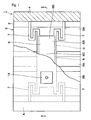
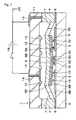
- Figs. 1 to 12 show a first embodiment of the present invention.
- a variable capacitance switch is described as an example of a variable capacitance element.
- reference numeral 1 denotes a variable capacitance switch
- reference numeral 2 denotes a substrate that forms a main part of the variable capacitance switch 1.
- the substrate 2 is made of, for example, high resistive monocrystal silicon material, insulating glass material, or the like.
- Reference numeral 3 denotes a transmission line which is provided as a fixed electrode on the substrate 2.
- the transmission 3 is composed of, for example, a plurality of metal films, etc., and is formed as a coplanar line for transmitting high frequency signals such as microwaves and milliwaves.
- the transmission line 3 is constituted by a central conductor 3A which extends in the front and back directions in Fig. 1, and ground conductors 3B which are disposed to the left side and right side of the central conductor 3A, and which are connected to the ground.
- Reference numeral 4 denotes, for example, two supporting portions which are provided on the substrate 2 in a protruding manner. To be more specific, the supporting portions are provided on both the right side and the left side of the transmission line 3 respectively.
- Each supporting portion 4 is made of, for example, low resistive monocrystal silicon material or the like, and is formed by means of an etching process, or the like, with a movable part 6 and support beams 7, which are described later.
- the supporting portion 4 is fixedly bonded to the substrate 2 by using, for example, an adhesive 5 such as polyimide resin.
- Reference numeral 6 denotes a movable part which is disposed above the upper surface of the substrate 2 so as to be displaced.
- the movable part 6 is made of, for example, resistive monocrystal silicon material or the like, and is formed into an approximately quadrangle plate having, for example, a thickness of approximately 20 to 80 ⁇ m.
- the movable part 6 is supported above the substrate 2 by the support beams 7, which is described later, and opposes a longitudinal intermediate region of the transmission line 3.
- the movable part 6 is displaced in a direction (a direction in which the movable part 6 is moved close to or away from the transmission line 3)perpendicular to the substrate 2.
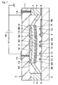
- the movable part 6 is vertically moved between a signal cutoff position (see Fig. 2) at which a high frequency signal on the transmission line 3 is cut off or blocked by a movable electrode 9, which is described later, and a signal passage position (see Fig. 5) which allows the high frequency signal to pass through the longitudinal intermediate region of the transmission line 3.
- a region of the movable part 6 which faces the conductors 3A and 3B of the transmission line 3 serves as a quadrangle conductor facing surface 6A.
- an insulating film 8, which is described later, and the movable part 9 are stacked.
- a region of the movable part 6 which faces a cover part 11, which is described later, serves as a back face 6B.
- Reference numeral 7 denotes, for example, four support beams which are each provided between each of four corners of the movable part 6 and each supporting portion 4.
- Each support beam 7 is made of, for example, low resistive monocrystal silicon material or the like, and is bent in a crank form, as shown in Figs. 1 and 2.
- Each support beam 7 warps to be deformed in an upward-downward direction in Fig. 2 perpendicular to the substrate 2, whereby the movable part 6 is supported so as to be displaced in the direction.
- the support beam 7 When the movable part 6 is at the signal cutoff position, the support beam 7 is maintained in a warping deformed (elastically deformed) state in a direction away from the transmission line 3. Its resilience (spring force) causes the movable part 6, etc., to apply a force to the transmission line 3. Therefore, when no power is supplied between a driving electrode 13, which is described later, and the movable part 6, the spring force of each support beam 7 maintains the movable electrode 9 to halt at a position (signal cutoff position) abutting against a stopper 10, which is described later.
- Reference numeral 8 denotes an insulating film which is provided as a warp adjusting film on the conductor facing surface 6A of the movable part 6.
- the insulating film 8 is formed by an insulating thin film of, for example, silicon oxide (SiO 2 ) or the like. It covers approximately the entirety of the conductor facing surface 6A of the movable part 6, having a thickness of, for example, approximately 0.1 to 10 ⁇ m.
- the insulating film 8 is disposed between the movable part 6 and the movable electrode 9, and provides insulation therebetween. In addition, by causing a compressive stress to operate on the movable part 6, the insulating film 8 adjusts the direction of a warp occurring in the entirety of the movable part 6, the insulating film 8, and the movable electrode 9. This constantly maintains all of them in a state in which they warp in a convex form toward the transmission line 3.
- the movable part 6, the insulating film 8, and the movable electrode 9 are formed so that a contributing component of a thermal stress, generated by differences in thermal expansion among the movable part 6, the insulating film 8, and the movable electrode 9, is small for an internal stress generated when the insulating film 8 and the movable electrode 9 are formed on the movable part 6.
- a total stress of the internal stress and the thermal stress can be designed so as to constantly maintain the warping direction of the movable part 6 to be unidirectional for a change in temperature, etc.
- variable capacitance switch 1 This allows the variable capacitance switch 1 to stably maintain a state in which, for a change in temperature of, for example, approximately -50 to 150°C, the movable part 6, etc., warps in a downwardly convex form toward the transmission line 3. This can prevent the warping direction from changing.
- Reference numeral 9 denotes a movable electrode provided to the conductor facing surface 6A with the insulating film 8 disposed therebetween.
- the movable electrode 9 is formed by a three-layer thin metal film obtained by stacking, for example, an adhesion layer of titanium, chromium, or the like, a barrier layer of platinum, palladium, or the like, and an electrode layer of gold or the like.
- the movable electrode 9 is formed having a thickness of, for example, approximately 0.1 to 5 ⁇ m, and is disposed in a position for covering the conductor facing surface 6A of the movable part 6.
- the movable electrode 9 moves close to the intermediate portion of the transmission line 3 at the signal cutoff position and moves away from the transmission line 3 at the signal passage position, whereby the capacitance between the movable electrode 9 and the transmission line 3 is changed.
- This allows the resonant frequency of the transmission line 3 to change in accordance with the position of the movable electrode 9.
- a high frequency signal transmitted on the transmission line 3 is cut off at the position of the movable electrode 9 in accordance with the resonant frequency, or passes at this position.
- the movable electrode 9 can perform a switching operation.
- the compressive stress of the insulating film 8 maintains the movable electrode 9 to warp in a convex form toward the transmission line 3, with the movable part 6.
- a central portion 9A of the movable electrode 9 more projects than peripheral portions 9B toward the transmission line 3.
- the central portion 9A, or the like, of the movable electrode 9 can be stably brought to halt at a position close the central conductor 3A of the transmission line 3.
- the capacitance between the movable electrode 9 and the transmission line 3, the resonant frequency of the transmission line 3, etc. can be accurately set, whereby the high frequency signal can be stably cut off.
- Reference numeral 10 denotes insular stoppers provided at plural positions of the transmission line 3.
- Each stopper 10 is formed by etching an insulating film of, for example, silicon oxide, and is formed in a portion of the surface of the transmission line 3, as shown in Figs. 2 and 3.
- the stopper 10 upward projects from the surface of the transmission line 3 to the movable electrode 9. Its projecting end abuts on the movable electrode 9 at the signal cutoff position. This allows the stopper 10 to maintain the movable part 6, the movable electrode 9, etc., to which force is applied by each support beam 7, at a halt at the signal cutoff position. In this state, the stopper 10 establishes insulation between the transmission line 3 and the movable electrode 9.
- Reference numeral 11 denotes the cover part, which is provided as another substrate to the substrate 2, with each supporting portion 4 provided therebetween.
- the cover part 11 is made of, for example, insulating glass material, high resistive silicon material, or the like.
- the cover part 11 is joined to one end of the supporting portion 4 by means of anode coupling, and is disposed opposite the substrate 2, with the movable part 6 provided therebetween.
- Reference numerals 12 denotes insular stoppers integrally formed at plural points of the cover part 11 at positions opposing the back face 6B of the movable part 6.
- the stopper 12 projects at a position closer to the movable part 6 compared with a driving electrode 13, which is described later. Its projecting end abuts on the movable part 6 at the signal passage position.
- the stopper 12 maintains the movable part 6, the movable electrode 9, etc., which are pulled to the driving electrode 13, to be at a halt at the signal passage position. It establishes insulation between the movable part 6 and the driving electrode 13.
- Reference numeral 13 denotes the driving electrode, which is provided as a driving means on the cover part 11 by using, for example, a metal film or the like.
- the driving electrode 13 is disposed between stoppers 12, and opposes the back face 6B of the movable part 6.
- the driving electrode 13 is connected to a power supply 15 through a lead electrode 14 provided on the cover part 11.
- the power supply 15 is connected to the movable part 6 through another lead electrodes 14, the supporting portions 4, the support beams 7, etc.
- variable capacitance switch 1 in this embodiment has the above-described configuration. Next, the case of using the variable capacitance switch 1 as a shunt switch is exemplified and its operation is described.
- the movable part 6 When the movable part 6 is at the signal cutoff position, by using the power supply 15 to supply power between the driving electrode 13 and the movable part 6, the movable part 6 is driven by an electrostatic force generated between them.
- the movable part 6, the movable electrode 9, etc., are displaced in a direction away from the transmission line 3. They halt at the signal passage position in a state pressed onto the stoppers 12.
- the impedances of opposing regions of both are sufficiently higher than the impedance (e.g., approximately 50 ⁇ ) of the transmission line 3. Accordingly, the high frequency signal transmitted through the transmission line 3 can pass at the position of the movable electrode 9, so that the variable capacitance switch 1 becomes a closed (ON) state.
- the spring forces of the support beams 7 drive the movable part 6 to be close to the transmission line 3.
- the resonant frequency of the transmission line 3 in the vicinity of the movable electrode 9 is changed to a predetermined frequency determined by the capacitance between the movable electrode 9 and the transmission line 3, and the inductance of the movable electrode 9.
- the impedance of the transmission line 3 becomes the minimum value in the vicinity of the movable electrode 9, and the high frequency signal transmitted through the transmission line 3 can be cut off (reflected) at the position of the movable electrode 9. This can switch the variable capacitance switch 1 to an open (OFF) state.
- the compressive stress of the insulating film 8 causes the movable part 6, the insulating film 8, and the movable electrode 9 to warp in a convex form toward the transmission line 3. Accordingly, when the movable part 6 is switched to the signal cutoff position, the central portion 9A, etc., of the movable electrode 9 can be stably maintained at an accurate position close to the central conductor 3A of the transmission line 3.
- the capacitance can be accurately changed so that the capacitance between the movable electrode 9 and the transmission line 3 is a predetermined value of capacitance.
- the resonant frequency of the transmission line 3 can be set with high accuracy in accordance with the value of the capacitance.
- the resonant frequency obtained when the movable part 6 is at the signal cutoff position and the frequency of the high frequency signal transmitted through the transmission line 3 can be set to be coincident with each other. This ensures that a signal cutoff operation can be performed.
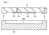
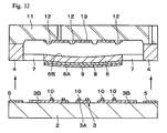
- variable capacitance switch 1 Next, a method for producing the variable capacitance switch 1 is described with reference to Figs. 6 to 12.
- the cover part 11 on which the stoppers 12, the driving electrode 13, etc., are provided is formed.
- a depression 16A having a predetermined depth is formed beforehand.
- the silicon plate 16 and the cover part 11 are joined to each other by a means such as anode coupling.
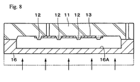
- the polishing step shown in Fig. 8 by polishing the silicon plate 16 from the opposite side of the cover part 11, the silicon plate 16 is formed to have a thickness of approximately 20 to 80 ⁇ m.
- the insulating-film forming step shown in Fig. 9 by using, for example, a means such as sputtering or thermal oxidation, to form a silicon oxide film on the polished surface of the silicon plate 16, and etching the film into a predetermined shape, the insulating film 8 is formed.
- a means such as sputtering or thermal oxidation
- the movable electrode 9 is formed.
- the compressive stress of the insulating film 8 cancels the tensile stress of the movable electrode 9, so that a total stress of the movable part 6, the insulating film 8, and the movable electrode 9 causes them to warp downwardly in a convex form.
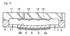
- the silicon plate 16 is patterned into a predetermined shape. Its portions are used to form the supporting portions 4, the movable part 6, and the support beams 7. Accordingly, the compressive stress of the insulating film 8 causes the patterned movable part 6 to warp downwardly in a convex form.
- etching such as reactive ion etching
- the variable capacitance switch 1 can be produced.
- the insulating film 8 is provided as a warp adjusting film on the conductor facing surface 6A of the movable part 6.
- the insulating film 8 can constantly warp the movable part 6 and the movable electrode 9 in a predetermined direction of warping in a downward convex form.
- the movable electrode 9 can be stably maintained at a predetermined position close to the central conductor 3A, etc., of the transmission line 3.
- the central portion 9A of the movable electrode 9 and the central conductor 3A of the transmission line 3, etc. can be moved close, having an accurate positional relationship.
- the insulating film 8 can prevent the warping direction of the movable part 6 and the movable electrode 9 from being changed due to a difference in their thermal expansion, and can prevent the positional relationship between the movable electrode 9 and the transmission line 3 from being shifted with the change.
- a capacitance obtained when the movable electrode 9 and the transmission line 3 are moved close to each other can be set to an accurate value, and the capacitance between them can be switched with high accuracy in accordance with the position of the movable part 6.
- This makes it possible to perform a stable switching operation for the high frequency signal, and the operation characteristics can be preferably maintained for a change in temperature, etc.
- the performance and reliability required for the switch can be improved.
- the movable part 6 and the insulating film 8 are formed so that a total stress of an internal stress and a thermal stress constantly maintains the warping direction of the movable part 6 to be constant for a change in temperature.
- the warping direction can be prevented from being varied by this stress. This enables the movable part 6 and the movable electrode 9 to constantly warp in a stable state in a predetermined direction.
- the insulating film 8 causes the movable part 6 and the movable electrode 9 to warp in a convex form toward the transmission line 3 by using a compressive stress.
- their central portions 6C and 9A can be set to project at a position close to the transmission line 3 compared with the peripheral portions 6D and 9B. Accordingly, when the movable part 6 is displaced toward the transmission line 3, the central portion 9A of the movable electrode 9 and the transmission line 3 are set to be closer to each other, so that the distance between both can be sufficiently decreased. Therefore, when the movable electrode 9 is moved close to or away from the transmission line 3, the capacitance between them can be greatly changed, whereby the switching operation can be stably performed in response to a change in capacitance.
- the insulating film 8 establishes insulation between the movable part 6 and the movable electrode 9, while adjusting the warping direction of them. This eliminates the need to provide another insulating structure or the like between the movable part 6, which is supplied with power from the power supply 15, and the movable electrode 9. Their construction can be simplified.
- the movable electrode 9 Since the transmission line 3 is provided with the stoppers 10, when the movable part 6 is displaced toward the transmission line 3, the movable electrode 9 is allowed to abut on the stoppers 10. This enables the stoppers 10 to stably maintain the movable electrode 9 at the signal cutoff position close to the transmission line 3, and the positional relationship (capacitance) between them can be accurately set. In addition, the movable electrode 9 can be prevented from being accidentally displaced due to vibration, a shock, etc., so that a vibration resistant characteristic can be enhanced. It is ensured that the stoppers 10 establish insulation between the movable electrode 9 and the transmission line 3, thus preventing short-circuiting between them.
- the stoppers 10 are formed to be insular, and they are locally disposed on the surface of the transmission line 3.
- an area in which the movable electrode 9 and each stopper 10 abut on each other can be reduced, whereby the variable capacitive switch 1 can be prevented from malfunctioning due to fixed bonding of both.
- gaps can be formed between the movable electrode 9 and the transmission line 3.
- the stoppers 10 can absorb the processing error or the like concerning the movable electrode 9 and the transmission line 3, and the positional relationship between both can be stably set.
- the cover part 11 is provided opposite the substrate 2, with the movable part 6 provided therebetween, and the cover part 11 is provided with the stoppers 12, which are insular.
- the stoppers 12 stably maintain the movable electrode 9 at the signal passage position, which is away from the transmission line 3. In this state, it is ensured that insulation is established between the movable part 6 and the driving electrode 13, and the movable part 6 can be prevented from being fixedly bonded to the stoppers 12. Since, in this case, the stoppers 12 are integrally formed with the cover part 11, processing and formation thereof can be efficiently performed.
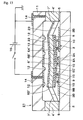
- Fig. 13 shows a second embodiment of the present invention.
- This embodiment is characterized in that a driving electrode is provided on also a movable part.
- a driving electrode is provided on also a movable part.
- Reference numeral 21 denotes a variable capacitance switch.
- the variable capacitance switch 21 includes, almost similarly to the first embodiment, a substrate 2, a transmission line 3, supporting portions 4', a movable part 6', support beams 7', an insulating film 8, a movable electrode 9, and a driving electrode 13.
- the movable part 6' has a conductor facing surface 6A', a back face 6B', a central portion 6C', and peripheral portions 6D'.
- a metal film or the like is used to provide a movable side driving electrode 22 on the back face 6B' of the movable part 6'.
- the driving electrode 22 and a fixed side driving electrode 13 constitute a driving means.
- the driving electrode 22 is also connected to a lead electrode 14 through a wiring pattern 23 (partially shown) provided along the supporting portions 4' and the support beams 7'.
- variable capacitance switch 21 When the variable capacitance switch 21 is switched, by using a power supply 15 to supply power between the driving electrodes 13 and 22 to generate an electrostatic force between them, the movable part 6' can be displaced to the signal passage position.
- the movable side driving electrode 22 is provided on the back face 6B' of the movable part 6.
- the variable capacitance switch 21 when the variable capacitance switch 21 is switched, by supplying power between the fixed side driving electrode 13 and the movable side driving electrode 22, the movable part 6', etc., can be smoothly displaced to the signal passage position.
- Fig. 14 shows a third embodiment of the present invention.
- This embodiment is characterized in that a movable part is set to warp in a concave form away from a fixed electrode.
- a movable part is set to warp in a concave form away from a fixed electrode.
- Reference numeral 31 denotes a variable capacitance switch.
- the variable capacitance switch 31 includes, almost similarly to the first embodiment, a substrate 2, a transmission line 3, support beams 7, a driving electrode 13, and a movable part 32, an insulating film 33, a movable electrode 34, etc., which are described later.
- Reference numeral 32 denotes a movable part which is disposed on the surface of the substrate 2 so as to be displaced.
- the movable part 32 is made of, for example, monocrystal silicon material or the like, almost similarly to the first embodiment.
- the movable part 32 is formed into a substantially quadrangle plate having a conductor facing surface 32A, a back face 32B, a central portion 32C, and peripheral portions 32D, and is supported by the support beams 7 so as to be displaced perpendicularly with respect to the substrate 2.
- the insulating film 33 and the movable electrode 34 which are almost similar to those in the first embodiment, are stacked on the conductor facing surface 32A of the movable part 32. However, both apply tensile stress to the movable part 32.
- the insulating films 8 are provided on the conductor facing surfaces 6A and 6A' of the movable parts 6 and 6'.
- the present invention is not limited thereto.
- the insulating films 8 and 33 which are made of, for example, silicon oxide, are used as warp-adjusting films.
- the warp-adjusting films may be made of other materials including silicon nitride (SiN).
- the warp-adjusting film may be made of conductive material.
- the stoppers 10 are provided on the transmission line 3 in a protruding manner.
- the present invention is not limited thereto.
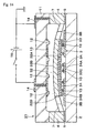
- the present invention may be formed into the modification shown in Fig. 15.
- stoppers 10' are provided on the surface of the movable electrode 9 in a protruding manner instead of the stoppers 10 on the side of the transmission line 3.
- both stoppers 10 and 10' may be provided.
- the stoppers 10 which are insular, are formed.
- the present invention is not limited thereto.
- insulating material other than silicon oxide may be used.
- an insulating film for covering the transmission line 3 may be formed and directly used without being etched.
- the driving electrode 13 is provided on the cover part 11.
- the present invention is not limited thereto.
- a driving electrode may be provided on a substrate and a cover part or the like may not be used.
- the driving electrode opposes a movable part at a position different from a fixed electrode, and an electrostatic force displaces the movable part.
- variable capacitance switches 1, 21, and 31 have been described as examples of variable capacitance elements.
- the present invention is not limited thereto.
- the present invention may be applied to a variable capacitor in which the capacitance of a capacitor composed of a fixed electrode and a movable electrode is switched in accordance with the position of a movable part.
- a coplanar line is described as an example of the transmission line 3.
- the present invention is not limited thereto.
- the present invention may be formed for application to various types of transmission lines including a slot line, etc.
Landscapes
- Engineering & Computer Science (AREA)
- Power Engineering (AREA)
- Microelectronics & Electronic Packaging (AREA)
- Micromachines (AREA)
- Waveguide Switches, Polarizers, And Phase Shifters (AREA)
- Manufacture Of Switches (AREA)
Abstract
Description
Claims (9)
- A variable capacitance element comprising: a substrate; a fixed electrode provided on the substrate; a plate-like movable part provided, at a position opposing the fixed electrode, on the substrate so as to be displaced, the movable part being moved close to and away from the fixed electrode; a movable electrode provided in a region of the movable part which faces the fixed electrode, the movable electrode having a capacitance in conjunction with the fixed electrode which is changed when the movable electrode is moved close to or away from the fixed electrode; and driving means for driving the movable part in a direction in which the movable part is moved close to or away from the fixed electrode,
wherein the movable part is provided with a warp adjusting film by which a direction in which a central portion of the movable part warps with respect to peripheral portions thereof is constantly maintained to one of a direction of warping in a convex form toward the fixed electrode and a direction of warping in a concave form away from the fixed electrode. - The variable capacitance element according to Claim 1, wherein, when the sum of an internal stress generated in the formation of the warp adjusting film on the movable part and a thermal stress generated by a difference in thermal expansion between the movable part and the warp adjusting film is a total stress, the movable part and the warp adjusting film are formed so that, for a change in temperature, the total stress constantly maintains the warping direction of the movable part to be unidirectional.
- The variable capacitance element according to Claim 1 or 2, wherein the warp adjusting film is formed to warp the movable part in the direction of warping in the convex form toward the fixed electrode.
- The variable capacitance element according to Claim 1 or 2, wherein the warp adjusting film is an insulating film for covering, with a compressive stress, the region of the movable part which faces the fixed electrode, the movable electrode is provided on the movable part, with the insulating film provided therebetween, and the insulating film uses the compressive stress to warp the movable part and the movable electrode in the direction of warping in the convex form toward the fixed electrode.
- The variable capacitance element according to Claim 1 or 2, wherein the warp adjusting film is formed so as to warp the movable part in the direction of warping in the concave form away from the fixed electrode.
- The variable capacitance element according to Claim 1, 2, 3, 4, or 5, wherein, between the fixed electrode and the movable electrode, at least one member is provided with an insulating stopper which abuts on the other member when the movable part is displaced toward the fixed electrode.
- The variable capacitance element according to Claim 6, wherein the stopper is provided in a portion of a region where the fixed electrode and the movable part oppose each other.
- The variable capacitance element according to Claim 1, 2, 3, 4, 5, 6, or 7, wherein the fixed electrode is a transmission line for transmitting a high frequency signal.
- The variable capacitance element according to Claim 1, 2, 3, 4, 5, 6, 7, or 8, wherein, for said substrate, a different substrate is provided opposite said substrate, with the movable part provided therebetween, and the different substrate is provided with a driving electrode which forms the driving means and which uses an electrostatic force to displace the movable part.
Applications Claiming Priority (3)
| Application Number | Priority Date | Filing Date | Title |
|---|---|---|---|
| JP2003315423 | 2003-09-08 | ||
| JP2003315423 | 2003-09-08 | ||
| PCT/JP2004/009642 WO2005027257A1 (en) | 2003-09-08 | 2004-07-07 | Variable capacitance element |
Publications (3)
| Publication Number | Publication Date |
|---|---|
| EP1538691A1 true EP1538691A1 (en) | 2005-06-08 |
| EP1538691A4 EP1538691A4 (en) | 2005-09-28 |
| EP1538691B1 EP1538691B1 (en) | 2011-05-18 |
Family
ID=34308425
Family Applications (1)
| Application Number | Title | Priority Date | Filing Date |
|---|---|---|---|
| EP04747111A Expired - Lifetime EP1538691B1 (en) | 2003-09-08 | 2004-07-07 | Variable capacitance element |
Country Status (7)
| Country | Link |
|---|---|
| US (1) | US7054132B2 (en) |
| EP (1) | EP1538691B1 (en) |
| JP (1) | JP4107329B2 (en) |
| KR (1) | KR100609589B1 (en) |
| CN (1) | CN1310374C (en) |
| AT (1) | ATE510318T1 (en) |
| WO (1) | WO2005027257A1 (en) |
Families Citing this family (37)
| Publication number | Priority date | Publication date | Assignee | Title |
|---|---|---|---|---|
| FR2851368B1 (en) * | 2003-02-18 | 2008-03-07 | Agence Spatiale Europeenne | ELECTRONIC COMPONENTS COMPRISING MICRO ELECTROMECHANICAL CAPACITORS WITH ADJUSTABLE CAPABILITY |
| JP2006210843A (en) * | 2005-01-31 | 2006-08-10 | Fujitsu Ltd | Variable capacitor and manufacturing method thereof |
| FR2884960B1 (en) * | 2005-04-25 | 2007-07-06 | Commissariat Energie Atomique | ELECTROMECHANICAL MICRO-CAPACITOR WITH VARIABLE CAPACITY AND METHOD OF MANUFACTURING SUCH MICRO-CAPACITOR |
| JP2007167998A (en) * | 2005-12-20 | 2007-07-05 | Toshiba Corp | Device having beam structure and semiconductor device |
| US20070145523A1 (en) * | 2005-12-28 | 2007-06-28 | Palo Alto Research Center Incorporated | Integrateable capacitors and microcoils and methods of making thereof |
| JP2007273932A (en) * | 2006-03-06 | 2007-10-18 | Fujitsu Ltd | Variable capacitor and variable capacitor manufacturing method |
| JP2008085022A (en) * | 2006-09-27 | 2008-04-10 | Nikon Corp | Variable capacitor |
| TWI466374B (en) * | 2006-09-27 | 2014-12-21 | 尼康股份有限公司 | Electronic component, variable capacitor, microswitch, microswitch driving method, and MEMS type electronic component |
| JP4279308B2 (en) * | 2006-11-02 | 2009-06-17 | アルプス電気株式会社 | Variable capacitance element and variable capacitance device |
| JP4910679B2 (en) * | 2006-12-21 | 2012-04-04 | 株式会社ニコン | Variable capacitor, variable capacitor device, high frequency circuit filter and high frequency circuit |
| JP2008155342A (en) * | 2006-12-26 | 2008-07-10 | Nippon Telegr & Teleph Corp <Ntt> | Manufacturing method of fine structure |
| JP4611323B2 (en) * | 2007-01-26 | 2011-01-12 | 富士通株式会社 | Variable capacitor |
| JP2008258186A (en) * | 2007-03-30 | 2008-10-23 | Matsushita Electric Ind Co Ltd | Variable capacity device |
| CN101471183B (en) * | 2007-12-27 | 2012-06-06 | 汉王科技股份有限公司 | Regulating mechanism of capacitor |
| JP2009160677A (en) * | 2007-12-28 | 2009-07-23 | Yamaha Corp | Mems and its manufacturing method |
| WO2009113344A1 (en) * | 2008-03-11 | 2009-09-17 | 株式会社 村田製作所 | Variable capacitance element |
| US8339764B2 (en) | 2008-05-12 | 2012-12-25 | Nxp B.V. | MEMs devices |
| JP5314932B2 (en) * | 2008-05-26 | 2013-10-16 | 太陽誘電株式会社 | Electric micro mechanical switch |
| JP2010061976A (en) * | 2008-09-03 | 2010-03-18 | Toshiba Corp | Switch and esd protection element |
| US8543580B2 (en) * | 2008-12-23 | 2013-09-24 | Microsoft Corporation | Mining translations of web queries from web click-through data |
| WO2010137447A1 (en) * | 2009-05-29 | 2010-12-02 | 株式会社村田製作所 | Variable capacity element |
| US8362853B2 (en) * | 2009-06-19 | 2013-01-29 | Qualcomm Incorporated | Tunable MEMS resonators |
| JP5223793B2 (en) * | 2009-06-26 | 2013-06-26 | 富士通株式会社 | Variable capacitor |
| DE102009047599A1 (en) * | 2009-12-07 | 2011-06-09 | Ihp Gmbh - Innovations For High Performance Microelectronics / Leibniz-Institut Für Innovative Mikroelektronik | Electromechanical microswitch for switching an electrical signal, microelectromechanical system, integrated circuit and method for producing an integrated circuit |
| KR101104537B1 (en) * | 2010-05-28 | 2012-01-11 | 한국과학기술원 | Variable capacitors and driving method thereof |
| JP5593903B2 (en) * | 2010-07-16 | 2014-09-24 | 富士通株式会社 | Variable capacitance element |
| KR102005335B1 (en) * | 2011-09-02 | 2019-07-30 | 카벤디시 키네틱스, 인크. | Mems variable capacitor with enhanced rf performance |
| US20140103878A1 (en) | 2011-10-31 | 2014-04-17 | Powermag, LLC | Power conditioning and saving device |
| JPWO2014054751A1 (en) * | 2012-10-04 | 2016-08-25 | アルプス電気株式会社 | Variable capacitor |
| TW201428794A (en) * | 2013-01-02 | 2014-07-16 | Ind Tech Res Inst | Tunable capacitor |
| EP2969912A4 (en) | 2013-03-15 | 2016-11-09 | Wispry Inc | DEVICES AND METHODS FOR CONTROLLING AND SEPARATING ACTUATOR PLATES |
| JP5921477B2 (en) | 2013-03-25 | 2016-05-24 | 株式会社東芝 | MEMS element |
| CN103440985B (en) * | 2013-07-30 | 2016-08-10 | 清华大学 | A kind of linear adjustable MEMS capacitor of multi-electrode |
| US20160099112A1 (en) * | 2014-10-03 | 2016-04-07 | wiSpry, Inc. . | Systems, devices, and methods to reduce dielectric charging in micro-electro-mechanical systems devices |
| FR3051458B1 (en) * | 2016-05-20 | 2020-09-04 | Univ Limoges | MICROELECTROMECHANICAL RADIOFREQUENCY VARIABLE SWITCH |
| DE102017109226A1 (en) * | 2017-04-28 | 2018-10-31 | Testo SE & Co. KGaA | Deep-frying oil and / or frying fat sensor for determining a frying oil and / or frying fat quality |
| JP7366706B2 (en) * | 2019-11-22 | 2023-10-23 | 東プレ株式会社 | capacitive switch |
Family Cites Families (9)
| Publication number | Priority date | Publication date | Assignee | Title |
|---|---|---|---|---|
| US5479042A (en) | 1993-02-01 | 1995-12-26 | Brooktree Corporation | Micromachined relay and method of forming the relay |
| US5526172A (en) | 1993-07-27 | 1996-06-11 | Texas Instruments Incorporated | Microminiature, monolithic, variable electrical signal processor and apparatus including same |
| US5901031A (en) * | 1995-02-01 | 1999-05-04 | Murata Manufacturing Co., Ltd. | Variable capacitor |
| JPH11274805A (en) * | 1998-03-20 | 1999-10-08 | Ricoh Co Ltd | High frequency switch, manufacturing method, and integrated high frequency switch array |
| US6020564A (en) | 1998-06-04 | 2000-02-01 | Wang Electro-Opto Corporation | Low-voltage long life electrostatic microelectromechanical system switches for radio-frequency applications |
| US6242989B1 (en) | 1998-09-12 | 2001-06-05 | Agere Systems Guardian Corp. | Article comprising a multi-port variable capacitor |
| JP3119255B2 (en) | 1998-12-22 | 2000-12-18 | 日本電気株式会社 | Micromachine switch and method of manufacturing the same |
| EP1343190A3 (en) * | 2002-03-08 | 2005-04-20 | Murata Manufacturing Co., Ltd. | Variable capacitance element |
| JP4151338B2 (en) * | 2002-07-30 | 2008-09-17 | 松下電器産業株式会社 | Variable capacitance element and method for forming the same |
-
2004
- 2004-07-07 AT AT04747111T patent/ATE510318T1/en not_active IP Right Cessation
- 2004-07-07 US US10/535,861 patent/US7054132B2/en not_active Expired - Fee Related
- 2004-07-07 JP JP2005513816A patent/JP4107329B2/en not_active Expired - Fee Related
- 2004-07-07 KR KR1020057008740A patent/KR100609589B1/en not_active Expired - Fee Related
- 2004-07-07 CN CNB2004800013557A patent/CN1310374C/en not_active Expired - Fee Related
- 2004-07-07 EP EP04747111A patent/EP1538691B1/en not_active Expired - Lifetime
- 2004-07-07 WO PCT/JP2004/009642 patent/WO2005027257A1/en not_active Ceased
Also Published As
| Publication number | Publication date |
|---|---|
| JP4107329B2 (en) | 2008-06-25 |
| WO2005027257A1 (en) | 2005-03-24 |
| ATE510318T1 (en) | 2011-06-15 |
| JPWO2005027257A1 (en) | 2006-11-24 |
| EP1538691A4 (en) | 2005-09-28 |
| CN1310374C (en) | 2007-04-11 |
| KR20050086669A (en) | 2005-08-30 |
| CN1706066A (en) | 2005-12-07 |
| US20060056132A1 (en) | 2006-03-16 |
| EP1538691B1 (en) | 2011-05-18 |
| US7054132B2 (en) | 2006-05-30 |
| KR100609589B1 (en) | 2006-08-08 |
Similar Documents
| Publication | Publication Date | Title |
|---|---|---|
| EP1538691B1 (en) | Variable capacitance element | |
| US7242273B2 (en) | RF-MEMS switch and its fabrication method | |
| US6833985B2 (en) | Variable capacitance element | |
| US8390173B2 (en) | MEMS switch and method of manufacturing the MEMS switch | |
| JP3402642B2 (en) | Electrostatic drive type relay | |
| EP1602624A1 (en) | Mems element and method of producing the same, and diffraction type mems element | |
| WO2009153757A1 (en) | Piezoelectric bimorph switch | |
| EP1788603B1 (en) | RF MEMS switch and method for fabricating the same | |
| JP3053069B2 (en) | Laminated actuator and its wiring method | |
| US7145284B2 (en) | Actuator and micro-electromechanical system device | |
| KR950005004A (en) | Optical path control device for projection image display device and manufacturing method thereof | |
| US7554136B2 (en) | Micro-switch device and method for manufacturing the same | |
| JPH10149950A (en) | Variable capacitance capacitor | |
| WO2005059933A1 (en) | Displacing element | |
| JP2009252516A (en) | Mems switch | |
| US20070139599A1 (en) | Comb-type electrode structure capable of large linear-displacement motion | |
| JPH0714490A (en) | Electrostatic actuating relay | |
| JP4628275B2 (en) | Microswitching device and method for manufacturing microswitching device | |
| JP2021001965A (en) | Wavelength variable interference filter | |
| JP2010021252A (en) | Variable capacitance element, and method of manufacturing the same | |
| US20220371880A1 (en) | Piezoelectric actuator stack with tapered sidewall | |
| JPH11234083A (en) | Piezoelectric part and its manufacture | |
| JP2009252378A (en) | Mems switch | |
| WO2005052966A1 (en) | Displacement element | |
| JP2003188049A (en) | Variable capacitance capacitor |
Legal Events
| Date | Code | Title | Description |
|---|---|---|---|
| PUAI | Public reference made under article 153(3) epc to a published international application that has entered the european phase |
Free format text: ORIGINAL CODE: 0009012 |
|
| 17P | Request for examination filed |
Effective date: 20050405 |
|
| AK | Designated contracting states |
Kind code of ref document: A1 Designated state(s): AT BE BG CH CY CZ DE DK EE ES FI FR GB GR HU IE IT LI LU MC NL PL PT RO SE SI SK TR |
|
| AX | Request for extension of the european patent |
Extension state: AL HR LT LV MK |
|
| A4 | Supplementary search report drawn up and despatched |
Effective date: 20050816 |
|
| DAX | Request for extension of the european patent (deleted) | ||
| RAP1 | Party data changed (applicant data changed or rights of an application transferred) |
Owner name: MURATA MANUFACTURING CO., LTD. |
|
| GRAP | Despatch of communication of intention to grant a patent |
Free format text: ORIGINAL CODE: EPIDOSNIGR1 |
|
| GRAS | Grant fee paid |
Free format text: ORIGINAL CODE: EPIDOSNIGR3 |
|
| GRAA | (expected) grant |
Free format text: ORIGINAL CODE: 0009210 |
|
| AK | Designated contracting states |
Kind code of ref document: B1 Designated state(s): AT BE BG CH CY CZ DE DK EE ES FI FR GB GR HU IE IT LI LU MC NL PL PT RO SE SI SK TR |
|
| REG | Reference to a national code |
Ref country code: GB Ref legal event code: FG4D |
|
| REG | Reference to a national code |
Ref country code: CH Ref legal event code: EP |
|
| REG | Reference to a national code |
Ref country code: IE Ref legal event code: FG4D |
|
| REG | Reference to a national code |
Ref country code: DE Ref legal event code: R096 Ref document number: 602004032712 Country of ref document: DE Effective date: 20110630 |
|
| REG | Reference to a national code |
Ref country code: NL Ref legal event code: VDEP Effective date: 20110518 |
|
| PG25 | Lapsed in a contracting state [announced via postgrant information from national office to epo] |
Ref country code: SE Free format text: LAPSE BECAUSE OF FAILURE TO SUBMIT A TRANSLATION OF THE DESCRIPTION OR TO PAY THE FEE WITHIN THE PRESCRIBED TIME-LIMIT Effective date: 20110518 Ref country code: PT Free format text: LAPSE BECAUSE OF FAILURE TO SUBMIT A TRANSLATION OF THE DESCRIPTION OR TO PAY THE FEE WITHIN THE PRESCRIBED TIME-LIMIT Effective date: 20110919 |
|
| PG25 | Lapsed in a contracting state [announced via postgrant information from national office to epo] |
Ref country code: BE Free format text: LAPSE BECAUSE OF FAILURE TO SUBMIT A TRANSLATION OF THE DESCRIPTION OR TO PAY THE FEE WITHIN THE PRESCRIBED TIME-LIMIT Effective date: 20110518 Ref country code: AT Free format text: LAPSE BECAUSE OF FAILURE TO SUBMIT A TRANSLATION OF THE DESCRIPTION OR TO PAY THE FEE WITHIN THE PRESCRIBED TIME-LIMIT Effective date: 20110518 Ref country code: FI Free format text: LAPSE BECAUSE OF FAILURE TO SUBMIT A TRANSLATION OF THE DESCRIPTION OR TO PAY THE FEE WITHIN THE PRESCRIBED TIME-LIMIT Effective date: 20110518 Ref country code: ES Free format text: LAPSE BECAUSE OF FAILURE TO SUBMIT A TRANSLATION OF THE DESCRIPTION OR TO PAY THE FEE WITHIN THE PRESCRIBED TIME-LIMIT Effective date: 20110829 Ref country code: GR Free format text: LAPSE BECAUSE OF FAILURE TO SUBMIT A TRANSLATION OF THE DESCRIPTION OR TO PAY THE FEE WITHIN THE PRESCRIBED TIME-LIMIT Effective date: 20110819 Ref country code: CY Free format text: LAPSE BECAUSE OF FAILURE TO SUBMIT A TRANSLATION OF THE DESCRIPTION OR TO PAY THE FEE WITHIN THE PRESCRIBED TIME-LIMIT Effective date: 20110518 Ref country code: SI Free format text: LAPSE BECAUSE OF FAILURE TO SUBMIT A TRANSLATION OF THE DESCRIPTION OR TO PAY THE FEE WITHIN THE PRESCRIBED TIME-LIMIT Effective date: 20110518 |
|
| PG25 | Lapsed in a contracting state [announced via postgrant information from national office to epo] |
Ref country code: NL Free format text: LAPSE BECAUSE OF FAILURE TO SUBMIT A TRANSLATION OF THE DESCRIPTION OR TO PAY THE FEE WITHIN THE PRESCRIBED TIME-LIMIT Effective date: 20110518 |
|
| PG25 | Lapsed in a contracting state [announced via postgrant information from national office to epo] |
Ref country code: CZ Free format text: LAPSE BECAUSE OF FAILURE TO SUBMIT A TRANSLATION OF THE DESCRIPTION OR TO PAY THE FEE WITHIN THE PRESCRIBED TIME-LIMIT Effective date: 20110518 Ref country code: EE Free format text: LAPSE BECAUSE OF FAILURE TO SUBMIT A TRANSLATION OF THE DESCRIPTION OR TO PAY THE FEE WITHIN THE PRESCRIBED TIME-LIMIT Effective date: 20110518 |
|
| PG25 | Lapsed in a contracting state [announced via postgrant information from national office to epo] |
Ref country code: SK Free format text: LAPSE BECAUSE OF FAILURE TO SUBMIT A TRANSLATION OF THE DESCRIPTION OR TO PAY THE FEE WITHIN THE PRESCRIBED TIME-LIMIT Effective date: 20110518 Ref country code: PL Free format text: LAPSE BECAUSE OF FAILURE TO SUBMIT A TRANSLATION OF THE DESCRIPTION OR TO PAY THE FEE WITHIN THE PRESCRIBED TIME-LIMIT Effective date: 20110518 Ref country code: DK Free format text: LAPSE BECAUSE OF FAILURE TO SUBMIT A TRANSLATION OF THE DESCRIPTION OR TO PAY THE FEE WITHIN THE PRESCRIBED TIME-LIMIT Effective date: 20110518 Ref country code: RO Free format text: LAPSE BECAUSE OF FAILURE TO SUBMIT A TRANSLATION OF THE DESCRIPTION OR TO PAY THE FEE WITHIN THE PRESCRIBED TIME-LIMIT Effective date: 20110518 Ref country code: MC Free format text: LAPSE BECAUSE OF NON-PAYMENT OF DUE FEES Effective date: 20110731 |
|
| REG | Reference to a national code |
Ref country code: CH Ref legal event code: PL |
|
| PLBE | No opposition filed within time limit |
Free format text: ORIGINAL CODE: 0009261 |
|
| STAA | Information on the status of an ep patent application or granted ep patent |
Free format text: STATUS: NO OPPOSITION FILED WITHIN TIME LIMIT |
|
| 26N | No opposition filed |
Effective date: 20120221 |
|
| REG | Reference to a national code |
Ref country code: IE Ref legal event code: MM4A |
|
| PG25 | Lapsed in a contracting state [announced via postgrant information from national office to epo] |
Ref country code: CH Free format text: LAPSE BECAUSE OF NON-PAYMENT OF DUE FEES Effective date: 20110731 Ref country code: LI Free format text: LAPSE BECAUSE OF NON-PAYMENT OF DUE FEES Effective date: 20110731 |
|
| PG25 | Lapsed in a contracting state [announced via postgrant information from national office to epo] |
Ref country code: IT Free format text: LAPSE BECAUSE OF FAILURE TO SUBMIT A TRANSLATION OF THE DESCRIPTION OR TO PAY THE FEE WITHIN THE PRESCRIBED TIME-LIMIT Effective date: 20110518 |
|
| REG | Reference to a national code |
Ref country code: DE Ref legal event code: R097 Ref document number: 602004032712 Country of ref document: DE Effective date: 20120221 |
|
| PG25 | Lapsed in a contracting state [announced via postgrant information from national office to epo] |
Ref country code: IE Free format text: LAPSE BECAUSE OF NON-PAYMENT OF DUE FEES Effective date: 20110707 |
|
| PG25 | Lapsed in a contracting state [announced via postgrant information from national office to epo] |
Ref country code: LU Free format text: LAPSE BECAUSE OF NON-PAYMENT OF DUE FEES Effective date: 20110707 |
|
| PG25 | Lapsed in a contracting state [announced via postgrant information from national office to epo] |
Ref country code: BG Free format text: LAPSE BECAUSE OF FAILURE TO SUBMIT A TRANSLATION OF THE DESCRIPTION OR TO PAY THE FEE WITHIN THE PRESCRIBED TIME-LIMIT Effective date: 20110818 |
|
| PG25 | Lapsed in a contracting state [announced via postgrant information from national office to epo] |
Ref country code: TR Free format text: LAPSE BECAUSE OF FAILURE TO SUBMIT A TRANSLATION OF THE DESCRIPTION OR TO PAY THE FEE WITHIN THE PRESCRIBED TIME-LIMIT Effective date: 20110518 |
|
| PG25 | Lapsed in a contracting state [announced via postgrant information from national office to epo] |
Ref country code: HU Free format text: LAPSE BECAUSE OF FAILURE TO SUBMIT A TRANSLATION OF THE DESCRIPTION OR TO PAY THE FEE WITHIN THE PRESCRIBED TIME-LIMIT Effective date: 20110518 |
|
| REG | Reference to a national code |
Ref country code: FR Ref legal event code: PLFP Year of fee payment: 13 |
|
| PGFP | Annual fee paid to national office [announced via postgrant information from national office to epo] |
Ref country code: GB Payment date: 20160721 Year of fee payment: 13 Ref country code: DE Payment date: 20160722 Year of fee payment: 13 |
|
| PGFP | Annual fee paid to national office [announced via postgrant information from national office to epo] |
Ref country code: FR Payment date: 20160721 Year of fee payment: 13 |
|
| REG | Reference to a national code |
Ref country code: DE Ref legal event code: R119 Ref document number: 602004032712 Country of ref document: DE |
|
| GBPC | Gb: european patent ceased through non-payment of renewal fee |
Effective date: 20170707 |
|
| REG | Reference to a national code |
Ref country code: FR Ref legal event code: ST Effective date: 20180330 |
|
| PG25 | Lapsed in a contracting state [announced via postgrant information from national office to epo] |
Ref country code: DE Free format text: LAPSE BECAUSE OF NON-PAYMENT OF DUE FEES Effective date: 20180201 Ref country code: GB Free format text: LAPSE BECAUSE OF NON-PAYMENT OF DUE FEES Effective date: 20170707 |
|
| PG25 | Lapsed in a contracting state [announced via postgrant information from national office to epo] |
Ref country code: FR Free format text: LAPSE BECAUSE OF NON-PAYMENT OF DUE FEES Effective date: 20170731 |