EP1538678A2 - LDMOS structure and method of making the same - Google Patents
LDMOS structure and method of making the same Download PDFInfo
- Publication number
- EP1538678A2 EP1538678A2 EP04106161A EP04106161A EP1538678A2 EP 1538678 A2 EP1538678 A2 EP 1538678A2 EP 04106161 A EP04106161 A EP 04106161A EP 04106161 A EP04106161 A EP 04106161A EP 1538678 A2 EP1538678 A2 EP 1538678A2
- Authority
- EP
- European Patent Office
- Prior art keywords
- source
- diffusion
- opening
- polysilicon gate
- gate layer
- Prior art date
- Legal status (The legal status is an assumption and is not a legal conclusion. Google has not performed a legal analysis and makes no representation as to the accuracy of the status listed.)
- Granted
Links
Images


Classifications
-
- H—ELECTRICITY
- H10—SEMICONDUCTOR DEVICES; ELECTRIC SOLID-STATE DEVICES NOT OTHERWISE PROVIDED FOR
- H10D—INORGANIC ELECTRIC SEMICONDUCTOR DEVICES
- H10D30/00—Field-effect transistors [FET]
- H10D30/60—Insulated-gate field-effect transistors [IGFET]
- H10D30/64—Double-diffused metal-oxide semiconductor [DMOS] FETs
- H10D30/65—Lateral DMOS [LDMOS] FETs
-
- H—ELECTRICITY
- H10—SEMICONDUCTOR DEVICES; ELECTRIC SOLID-STATE DEVICES NOT OTHERWISE PROVIDED FOR
- H10D—INORGANIC ELECTRIC SEMICONDUCTOR DEVICES
- H10D30/00—Field-effect transistors [FET]
- H10D30/01—Manufacture or treatment
- H10D30/021—Manufacture or treatment of FETs having insulated gates [IGFET]
- H10D30/028—Manufacture or treatment of FETs having insulated gates [IGFET] of double-diffused metal oxide semiconductor [DMOS] FETs
-
- H—ELECTRICITY
- H10—SEMICONDUCTOR DEVICES; ELECTRIC SOLID-STATE DEVICES NOT OTHERWISE PROVIDED FOR
- H10D—INORGANIC ELECTRIC SEMICONDUCTOR DEVICES
- H10D62/00—Semiconductor bodies, or regions thereof, of devices having potential barriers
- H10D62/10—Shapes, relative sizes or dispositions of the regions of the semiconductor bodies; Shapes of the semiconductor bodies
- H10D62/124—Shapes, relative sizes or dispositions of the regions of semiconductor bodies or of junctions between the regions
- H10D62/126—Top-view geometrical layouts of the regions or the junctions
- H10D62/127—Top-view geometrical layouts of the regions or the junctions of cellular field-effect devices, e.g. multicellular DMOS transistors or IGBTs
-
- H—ELECTRICITY
- H10—SEMICONDUCTOR DEVICES; ELECTRIC SOLID-STATE DEVICES NOT OTHERWISE PROVIDED FOR
- H10D—INORGANIC ELECTRIC SEMICONDUCTOR DEVICES
- H10D62/00—Semiconductor bodies, or regions thereof, of devices having potential barriers
- H10D62/10—Shapes, relative sizes or dispositions of the regions of the semiconductor bodies; Shapes of the semiconductor bodies
- H10D62/13—Semiconductor regions connected to electrodes carrying current to be rectified, amplified or switched, e.g. source or drain regions
- H10D62/149—Source or drain regions of field-effect devices
- H10D62/151—Source or drain regions of field-effect devices of IGFETs
- H10D62/152—Source regions of DMOS transistors
- H10D62/153—Impurity concentrations or distributions
-
- H—ELECTRICITY
- H10—SEMICONDUCTOR DEVICES; ELECTRIC SOLID-STATE DEVICES NOT OTHERWISE PROVIDED FOR
- H10D—INORGANIC ELECTRIC SEMICONDUCTOR DEVICES
- H10D30/00—Field-effect transistors [FET]
- H10D30/60—Insulated-gate field-effect transistors [IGFET]
- H10D30/64—Double-diffused metal-oxide semiconductor [DMOS] FETs
- H10D30/66—Vertical DMOS [VDMOS] FETs
-
- H—ELECTRICITY
- H10—SEMICONDUCTOR DEVICES; ELECTRIC SOLID-STATE DEVICES NOT OTHERWISE PROVIDED FOR
- H10D—INORGANIC ELECTRIC SEMICONDUCTOR DEVICES
- H10D62/00—Semiconductor bodies, or regions thereof, of devices having potential barriers
- H10D62/10—Shapes, relative sizes or dispositions of the regions of the semiconductor bodies; Shapes of the semiconductor bodies
- H10D62/13—Semiconductor regions connected to electrodes carrying current to be rectified, amplified or switched, e.g. source or drain regions
- H10D62/149—Source or drain regions of field-effect devices
- H10D62/151—Source or drain regions of field-effect devices of IGFETs
-
- H—ELECTRICITY
- H10—SEMICONDUCTOR DEVICES; ELECTRIC SOLID-STATE DEVICES NOT OTHERWISE PROVIDED FOR
- H10D—INORGANIC ELECTRIC SEMICONDUCTOR DEVICES
- H10D62/00—Semiconductor bodies, or regions thereof, of devices having potential barriers
- H10D62/80—Semiconductor bodies, or regions thereof, of devices having potential barriers characterised by the materials
- H10D62/83—Semiconductor bodies, or regions thereof, of devices having potential barriers characterised by the materials being Group IV materials, e.g. B-doped Si or undoped Ge
-
- H—ELECTRICITY
- H10—SEMICONDUCTOR DEVICES; ELECTRIC SOLID-STATE DEVICES NOT OTHERWISE PROVIDED FOR
- H10D—INORGANIC ELECTRIC SEMICONDUCTOR DEVICES
- H10D64/00—Electrodes of devices having potential barriers
- H10D64/20—Electrodes characterised by their shapes, relative sizes or dispositions
- H10D64/23—Electrodes carrying the current to be rectified, amplified, oscillated or switched, e.g. sources, drains, anodes or cathodes
- H10D64/251—Source or drain electrodes for field-effect devices
- H10D64/257—Source or drain electrodes for field-effect devices for lateral devices wherein the source or drain electrodes are characterised by top-view geometrical layouts, e.g. interdigitated, semi-circular, annular or L-shaped electrodes
-
- H—ELECTRICITY
- H10—SEMICONDUCTOR DEVICES; ELECTRIC SOLID-STATE DEVICES NOT OTHERWISE PROVIDED FOR
- H10D—INORGANIC ELECTRIC SEMICONDUCTOR DEVICES
- H10D64/00—Electrodes of devices having potential barriers
- H10D64/20—Electrodes characterised by their shapes, relative sizes or dispositions
- H10D64/23—Electrodes carrying the current to be rectified, amplified, oscillated or switched, e.g. sources, drains, anodes or cathodes
- H10D64/251—Source or drain electrodes for field-effect devices
- H10D64/258—Source or drain electrodes for field-effect devices characterised by the relative positions of the source or drain electrodes with respect to the gate electrode
-
- H—ELECTRICITY
- H10—SEMICONDUCTOR DEVICES; ELECTRIC SOLID-STATE DEVICES NOT OTHERWISE PROVIDED FOR
- H10D—INORGANIC ELECTRIC SEMICONDUCTOR DEVICES
- H10D64/00—Electrodes of devices having potential barriers
- H10D64/60—Electrodes characterised by their materials
- H10D64/62—Electrodes ohmically coupled to a semiconductor
Definitions
- the present invention relates to integrated circuits, and in particular to an DMOS structure of enhanced characteristics in withstanding high currents while retaining a low on-resistance and which can be integrated with enhanced compactness.
- An DMOS structure is constituted by a drain region, a source region and a gate defined over a channel region.
- the source-body region that is realized in correspondence of a purposely defined opening of a polysilicon gate layer, includes a P-body diffusion formed inside an N- pocket, a single or, more commonly, a shallow N- and a deeper N+ source diffusions are formed in succession in the P-body region, by successive implants, self-aligned to the definition edges of the poly (gate) opening and to dielectric spacers successively formed there along, respectively, according to well known VLSI and ULSI fabrication techniques.
- a source contact is established on the N+ source diffusion (of course the types of conductivities are inverted in the case of a P-channel device).
- ULSI DMOS structures (N-channel or P-channel) generally have source regions provided with a plurality of minimum size contacts formed on the (N+ or P+) source diffusions and larger size contacts on the local plug diffusions (p+ or N+) of electrical connection to the body region. The local short-circuit between the P+ and N+ diffusions is thence established through the common source contact metallization.
- an electrically conductive layer of silicide formed in a self-aligned manner (from where the acronym SAlicide) over the whole silicon surface in the source region area, effectively short-circuits the source (N+ or P+) diffusion and the plug diffusion (P+ or N+) of electrical connection of the underlying body region, while the electric current eventually flows through one or more contacts formed on the silicide layer.
- at least a source contact is projectively formed over the area of the plug diffusion (P+ or N+) of electrical connection.
- the layout of the contacts in the source region influences the on-resistance of integrated DMOS devices.
- the on-resistance per unit area of integration is proportional to the "pitch" distance between the source contacts and the drain contacts, and inversely proportional to the width W of the drain and source regions.
- the on-resistance per unit area of integration may be lowered only by reducing as much as possible the distance between such regions within the limits imposed by the fabrication technology.
- the layout of an DMOS structure is practically symmetrical for p-channel and n-channel devices.
- SAlicide layer onto which forming at least a source-body contact and if required a plurality of source contacts formed spacingly along the central axis in the width direction W of the opening through the polysilicon, has significantly helped in enhancing the resulting conductivity of an integrated DMOS structure by accomplishing a most even distribution of the lines of current in the silicon toward the multiple source contacts and in reducing the width and pitch of the structure for comparable electrical performances, has imposed the requisite of providing for the presence of a continuous heavily doped superficial region within the source region definition opening through the polysilicon, in order to achieve an optimization of conduction characteristics.
- formation of a highly conductive layer of SAlicide thereon is favored by the presence of heavily doped silicon at the surface.
- Such a requisite is generally fulfilled by the continuity of the relatively heavily doped source area implant (N+) surrounding the area of definition of the body contact plug diffusion (that need to be masked from the heavy source implant by a resist cap or island) in order to ensure continuity of a heavily doped silicon surface area along the W direction of the opening through the polysilicon layer.
- P+ dopant
- N+ polysilicon
- the width of the opening in the polysilicon must be necessarily made sufficiently large for ensuring a sufficient distance of separation between the side of the central mask window used for implanting the body contact plug diffusion dopant from the definition edge of the poly (gate), inevitably limits the possibility of reducing the width in the pitch direction of the elongated openings through the polysilicon gate layer.
- the pitch of integration of an DMOS structure may be further significantly reduced and/or the on-resistance per unit area of integration of the structure significantly increased while preserving adequate voltage withstanding characteristics of the integrated structure, by the ability provided by this invention of reducing the width (in the pitch direction) of the opening through the polysilicon gate layer in correspondence of each body-source island far beyond the limits imposed in the structures made according to the prior art, for the reasons mentioned above.
- the invention rests on a finding that continuity of the heavily doped superficial silicon region along the axis of the elongated source island openings through the polysilicon gate layer in the width direction (W) of the integrated structure, no longer needs to be assured by defining it with a width (in the pitch direction) sufficiently large to account for the overlay of two distinct and relatively critical masks, namely: the source implant mask and the body contacting plug diffusion implant contact opening mask, which was responsible of limiting the possibility of restricting the opening through the polysilicon gate layer in order to safely ensure an appropriate distance of the body connection plug diffusion dopant profile from the defmition edges of the polysilicon.
- the body connection plug diffusion implant area is, according to this invention, defined by way of a mutual orthogonality between two no longer critical masks that may both be defined at minimum linewidth of the fabrication process.
- the source implant mask defines within the opening through the polysilicon gate a certain area in the form of a strip orthogonal to the width direction (W) and extending across the opening through the polysilicon gate layer that is masked from the source implant and that therefore receives only a first shallow light doping (LDD) source implant before formation of the dielectric spacers on the definition edges of the opening through the polysilicon gate layer.
- W width direction
- LDD shallow light doping
- such an orthogonal masked strip may be defined at minimum linewidth of the fabrication process, however, the width of such a source implant mask extending across the opening through the polysilicon gate layer, that is orthogonally in respect of the width direction (W) of the integrated structure, may even be larger than the minimum linewidth with which will be successively defined the source contact metal.
- the mask of body connection plug diffusion area implant defining an implant window in the form of a continuous strip along the central axis in the width direction (W) of the opening through the polysilicon gate layer may be defined at minimum linewidth.
- the linewidth of definition of the two masks of heavy source implant area and of the body connection plug diffusion implant area may both be the same as the width of defmition of the source contact to be formed on the layer of salicide in correspondence of the body contact plug diffusion.
- the linewidth may be the minimum afforded by the fabrication process.
- the implanted dopant of the body connection plug diffusion is received along such a central strip of minimum linewidth also by the heavily doped silicon of the source region without inverting the type of conductivity thereof.
- the implant window of the body connection plug diffusion dopant as an orthogonal strip of minimum linewidth, instead of a centered island area, the need of accounting for an adequate overlay is eliminated and overall renders the two masks that define (at their crossover) the implant area of the plug diffusion no longer critical.
- any "necking" of the most conductive portion of the area of the successively deposited silicide layer that may be consequent of a reduced concentration of dopant present at the surface of the silicon from the diffusion profile line of the body contact play diffusion dopant to the edge of defmition of the gate polysilicon in correspondence of the orthogonal strip of definition of minimum linewidth of the source implant mask does not affect in any sensible manner the electrical conduction behavior (equipotentiality) of the source contacts and of the body-source short-circuiting provided by the silicide layer.
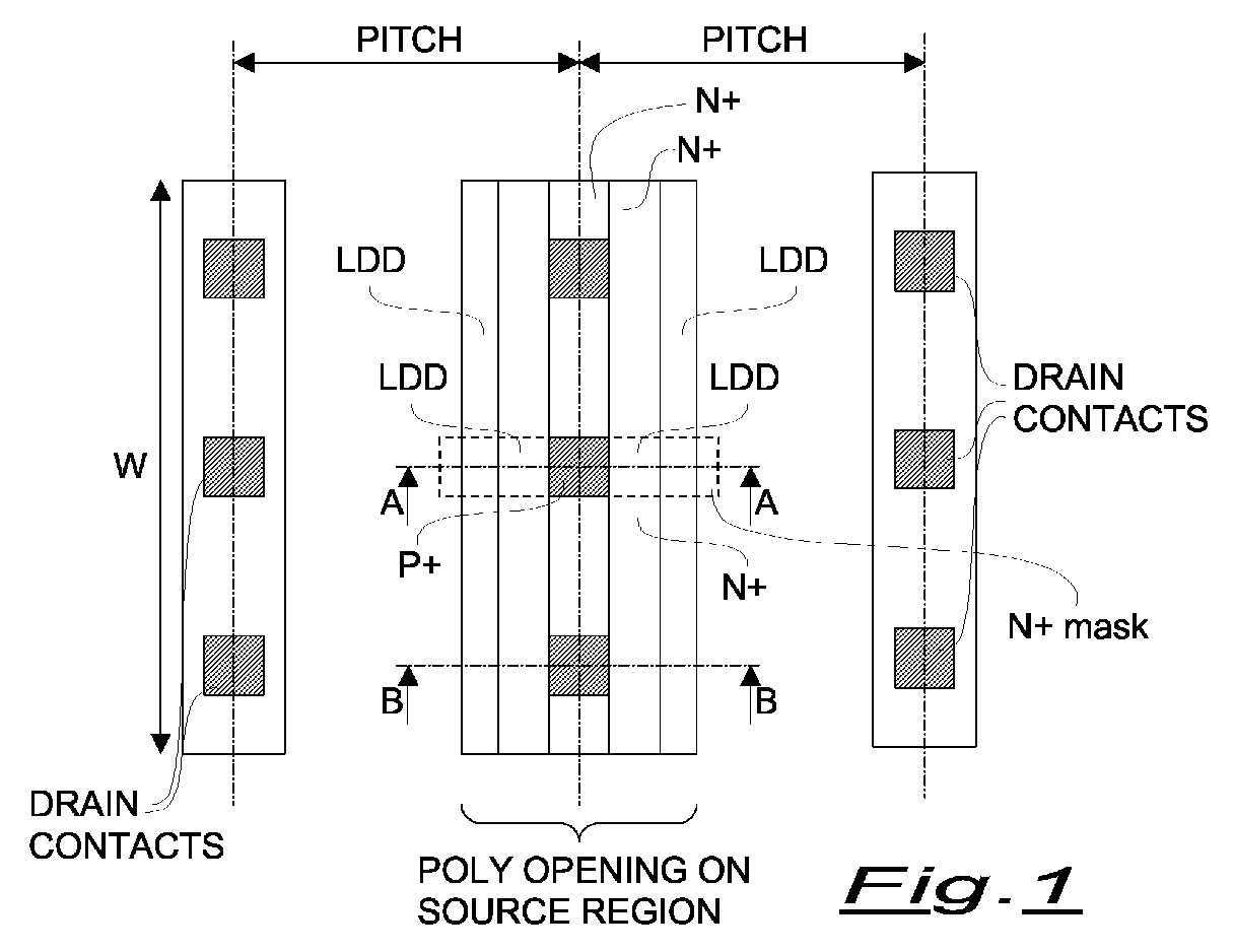
- FIG. 1 The basic layout view of an integrated LDMOS N-channel structure made according to the present invention is shown in Figure 1, while Figures 2 and 3 are partial cross sectional views along the section planes A-A and B-B, respectively.
- the N+ mask may be defined with the minimum linewidth of the process of fabrication, like the source contacts.
- Another feature of the structure of this invention is represented by the fact that the P+ mask that is used for implanting the P+ dopant in the crossover area with the N+ mask, for realizing the body connection plug diffusion P+ and which eventually also increases the total dopant species concentration in the silicon region extending along the central axis of the source region in the width direction W of the integrated structure though without inverting the type of conductivity conferred to it by the higher N+ source implant, is also defined with the minimum linewidth, centered about the central axis of the source region in the W direction.
- the body connection plug diffusion P+ is defined by way of the orthogonality of the two masks N+ and P+ (crossover area), without accounting for any overlay that by contrast was necessary to account for in the known process.
- the width of the longitudinal central strip of the N+ source region that eventually receives also the P+ dopant in an amount short of compensation of the N+ heavy source doping has minimum linewidth, like the N+ mask and the source contact mask.
- the width of the longitudinal central strip of the source region, receiving the heavy implants of dopants of opposite type of conductivities, because of the necessary overlays of about 0.1 ⁇ m on each side, would become 0.6 ⁇ m and by considering the spacers, the total width of the poly opening will be of about 1.2 ⁇ m.
- the novel method of this invention permits to narrow the width of the poly openings of source areas to about 0.8 ⁇ m, practically to 2/3 of the width that was necessary in the prior process.
- the minimum linewidth of definition used ranges from 0.3 to 0.8 ⁇ m
- the overlays in defining the width of the longitudinal central strip area of a source island range from 0.1 to 0.3 ⁇ m and the lateral extension of dielectric spacers may range from 0.2 to 0.9 ⁇ m.
- the novel approach of the present applicants to realize the required shotcircuiting of the body region to the source contacts permits to achieve a significative reduction of the width of the poly openings of the source islands and therefore a consistent shrinkage of the whole DMOS structure.
- the highly conductive silicide layer remains electrically continuous along the width direction W of the source region of the integrated LDMOS structure, notwithstanding the local discontinuity deliberately caused in the N+ source diffusion and the consequent presence of local lightly doped zones at the surface of the silicon, between the heavily doped central area of the P+ plug diffusion and the opposing edge of the gate electrode (POLY).
Landscapes
- Insulated Gate Type Field-Effect Transistor (AREA)
Abstract
Description
- the body mask which defines the opening through the polysilicon gate layer in correspondence in the source/body region of the structure;
- the contact (opening) and source (island) masks that are commonly designed at minimum lithographical dimension;
- the body contact mask, by which a sufficient effective distance from the polysilicon (gate electrode) edge of the "plug" of heavily doped silicon of type of conductivity opposite to that of the surrounding source region, reaching down in depth to contact the underlying body region, is defined to ensure adequate voltage withstanding characteristics.

Claims (4)
- A DMOS structure realized in a region of a first type of conductivity (N-pocket) of a semiconductor substrate and comprising a polysilicon gate layer, drain regions and source regions spacingly and parallelly extending in a first direction for a certain width (W) of integration of the DMOS structure, each source region being formed in correspondence of a purposely defined opening through said polysilicon gate layer, elongated in said width (W) direction of the integrated structure, wherein each of said source region comprisescharacterized in thata body diffusion (PBODY) of a second type of conductivity implanted in self-alignment to the definition edges of the opening through the polysilicon gate layer,a first source diffusion (LDD) of said first type of conductivity implanted in self-alignment to the definition edges of said opening through the polysilicon gate layer and a second heavily doped source diffusion (N+) implanted in self-alignment to the edges of dielectric spacers formed on the edges of definition of said opening in the polysilicon gate layer, except for a central area purposely masked from said second source implant (N+),a body connection plug diffusion (P+) of said second type of conductivity formed in said masked area, reaching down to said body diffusion (PBODY),a layer of silicide formed over the silicon surface of said second source diffusion (N+) and of said body connection plug diffusion (P+) and at least a source contact formed over said silicide layer in correspondence of said body connection plug diffusion (P+),said area of the silicon masked from said second source diffusion (N+) implant is in the form of a strip orthogonal to said width direction (W) and extends across the opening in the polysilicon gate layer;said masked area and the area of implant of the dopant of said body connection plug diffusion (P+) along the central axis of the opening in said width direction (W) being both defined with the same linewidth of defmition of said source contact.
- The DMOS structure according to claim 1, wherein said linewidth of definition is the minimum linewidth afforded by the fabrication process used for realizing the structure.
- A method of reducing the pitch of integration of a DMOS structure realized in a region of a first type of conductivity (N-pocket) of a semiconductor substrate and comprising a polysilicon gate layer, drain regions and source regions spacingly and parallelly extending in a first direction for a certain width (W) of integration of the structure, each source region being formed in correspondence of a purposely defined opening through said polysilicon gate layer, elongated in said width (W) direction of the integrated structure, each source region comprising a body diffusion (PBODY) of a second type of conductivity implanted in self-alignment to the definition edges of said opening through the polysilicon gate layer, a first source diffusion (LDD) of said first type of conductivity implanted in self-alignment to the definition edges of said opening through the polysilicon gate layer and a second source diffusion (N+) implanted in self-alignment to the edges of dielectric spacers formed on the edges of definition of said opening in the polysilicon gate layer, except for a central area purposely masked from said second source implant (N+), a body connection plug diffusion (P+) of said second type of conductivity formed in said masked area, reaching down to said body diffusion (PBODY), a layer of silicide formed over the silicon surface of said second source diffusion (N+) and of said body contact plug diffusion (P+) and at least a source contact formed over said silicide layer in correspondence of said body connection plug diffusion (P+), the method consisting in defining the implant area of said body connection plug diffusion (P+) in the crossover area of a (N+) implant mask of said second source diffusion defining a strip orthogonal to said width direction (W) extending across said opening in the polysilicon gate layer and of an implant mask of said body connection plug diffusion (P+) defming a strip of the same linewidth of said orthogonal strip of the implant mask of said second source diffusion and along the central axis of the opening in said width (W) direction.
- The method of claim 3, wherein said linewidth of definition is the minimum linewidth afforded by the fabrication process.
Priority Applications (1)
| Application Number | Priority Date | Filing Date | Title |
|---|---|---|---|
| EP04106161A EP1538678B1 (en) | 2003-12-05 | 2004-11-29 | DMOS structure and method of making the same |
Applications Claiming Priority (3)
| Application Number | Priority Date | Filing Date | Title |
|---|---|---|---|
| EP03425782 | 2003-12-05 | ||
| EP03425782A EP1538677A1 (en) | 2003-12-05 | 2003-12-05 | LDMOS structure and method of making the same |
| EP04106161A EP1538678B1 (en) | 2003-12-05 | 2004-11-29 | DMOS structure and method of making the same |
Publications (3)
| Publication Number | Publication Date |
|---|---|
| EP1538678A2 true EP1538678A2 (en) | 2005-06-08 |
| EP1538678A3 EP1538678A3 (en) | 2005-07-27 |
| EP1538678B1 EP1538678B1 (en) | 2008-07-16 |
Family
ID=34466361
Family Applications (1)
| Application Number | Title | Priority Date | Filing Date |
|---|---|---|---|
| EP04106161A Expired - Lifetime EP1538678B1 (en) | 2003-12-05 | 2004-11-29 | DMOS structure and method of making the same |
Country Status (1)
| Country | Link |
|---|---|
| EP (1) | EP1538678B1 (en) |
Cited By (1)
| Publication number | Priority date | Publication date | Assignee | Title |
|---|---|---|---|---|
| CN112071913A (en) * | 2020-09-08 | 2020-12-11 | 深圳基本半导体有限公司 | Silicon carbide planar gate MOSFET cell structure and manufacturing method |
Families Citing this family (1)
| Publication number | Priority date | Publication date | Assignee | Title |
|---|---|---|---|---|
| CN101673762B (en) * | 2008-09-09 | 2011-08-24 | 上海华虹Nec电子有限公司 | LDMOS transistor structure and fabrication method |
Family Cites Families (4)
| Publication number | Priority date | Publication date | Assignee | Title |
|---|---|---|---|---|
| JPS5688363A (en) * | 1979-12-20 | 1981-07-17 | Nec Corp | Field effect transistor |
| US5719421A (en) * | 1994-10-13 | 1998-02-17 | Texas Instruments Incorporated | DMOS transistor with low on-resistance and method of fabrication |
| US5825065A (en) * | 1997-01-14 | 1998-10-20 | Texas Instruments Incorporated | Low voltage DMOS transistor |
| EP1158583A1 (en) * | 2000-05-23 | 2001-11-28 | STMicroelectronics S.r.l. | Low on-resistance LDMOS |
-
2004
- 2004-11-29 EP EP04106161A patent/EP1538678B1/en not_active Expired - Lifetime
Cited By (1)
| Publication number | Priority date | Publication date | Assignee | Title |
|---|---|---|---|---|
| CN112071913A (en) * | 2020-09-08 | 2020-12-11 | 深圳基本半导体有限公司 | Silicon carbide planar gate MOSFET cell structure and manufacturing method |
Also Published As
| Publication number | Publication date |
|---|---|
| EP1538678A3 (en) | 2005-07-27 |
| EP1538678B1 (en) | 2008-07-16 |
Similar Documents
| Publication | Publication Date | Title |
|---|---|---|
| US7605040B2 (en) | Method of forming high breakdown voltage low on-resistance lateral DMOS transistor | |
| US10014381B2 (en) | Semiconductor power devices manufactured with self-aligned processes and more reliable electrical contacts | |
| KR100958421B1 (en) | Power device and manufacturing method thereof | |
| US7649225B2 (en) | Asymmetric hetero-doped high-voltage MOSFET (AH2MOS) | |
| US5102815A (en) | Method of fabricating a composite inverse T-gate metal oxide semiconductor device | |
| CN100585875C (en) | LDMOS transistor | |
| EP1577952B1 (en) | Method of making a high voltage insulated gate field-effect transistor | |
| US10069006B2 (en) | Semiconductor device with vertical field floating rings and methods of fabrication thereof | |
| US6093588A (en) | Process for fabricating a high voltage MOSFET | |
| US7671425B2 (en) | Semiconductor device and method of manufacturing the same | |
| US7696061B2 (en) | Semiconductor device and method for manufacturing same | |
| US12243939B2 (en) | Laterally diffused metal-oxide semiconductor (LDMOS) transistor with integrated back-gate | |
| KR100289049B1 (en) | Power device having double field plate structure | |
| EP1538677A1 (en) | LDMOS structure and method of making the same | |
| KR20000014215A (en) | Method for manufacturing the reliable lateral transistor | |
| EP1538678B1 (en) | DMOS structure and method of making the same | |
| JPH07263693A (en) | FET manufacturing method and integrated structure | |
| KR100272174B1 (en) | Lateral double-diffused mos transistor device and method for manufacturing the same | |
| KR100457907B1 (en) | Power transistors and method of fabricating the same | |
| EP1450411A1 (en) | MOS power device with high integration density and manufacturing process thereof | |
| KR20050101616A (en) | Method for manufacturing power mosfet | |
| JPH11297986A (en) | Mosfet | |
| JP2005175035A (en) | Method of manufacturing semiconductor device | |
| KR20000027642A (en) | Method of manufacturing semiconductor device | |
| KR19990085521A (en) | Power semiconductor device and manufacturing method |
Legal Events
| Date | Code | Title | Description |
|---|---|---|---|
| PUAI | Public reference made under article 153(3) epc to a published international application that has entered the european phase |
Free format text: ORIGINAL CODE: 0009012 |
|
| AK | Designated contracting states |
Kind code of ref document: A2 Designated state(s): AT BE BG CH CY CZ DE DK EE ES FI FR GB GR HU IE IS IT LI LU MC NL PL PT RO SE SI SK TR |
|
| AX | Request for extension of the european patent |
Extension state: AL HR LT LV MK YU |
|
| PUAL | Search report despatched |
Free format text: ORIGINAL CODE: 0009013 |
|
| AK | Designated contracting states |
Kind code of ref document: A3 Designated state(s): AT BE BG CH CY CZ DE DK EE ES FI FR GB GR HU IE IS IT LI LU MC NL PL PT RO SE SI SK TR |
|
| AX | Request for extension of the european patent |
Extension state: AL HR LT LV MK YU |
|
| 17P | Request for examination filed |
Effective date: 20060110 |
|
| AKX | Designation fees paid |
Designated state(s): DE FR GB IT |
|
| RTI1 | Title (correction) |
Free format text: DMOS STRUCTURE AND METHOD OF MAKING THE SAME |
|
| GRAP | Despatch of communication of intention to grant a patent |
Free format text: ORIGINAL CODE: EPIDOSNIGR1 |
|
| GRAS | Grant fee paid |
Free format text: ORIGINAL CODE: EPIDOSNIGR3 |
|
| GRAA | (expected) grant |
Free format text: ORIGINAL CODE: 0009210 |
|
| AK | Designated contracting states |
Kind code of ref document: B1 Designated state(s): DE FR GB IT |
|
| REG | Reference to a national code |
Ref country code: GB Ref legal event code: FG4D |
|
| REF | Corresponds to: |
Ref document number: 602004015050 Country of ref document: DE Date of ref document: 20080828 Kind code of ref document: P |
|
| PLBE | No opposition filed within time limit |
Free format text: ORIGINAL CODE: 0009261 |
|
| STAA | Information on the status of an ep patent application or granted ep patent |
Free format text: STATUS: NO OPPOSITION FILED WITHIN TIME LIMIT |
|
| 26N | No opposition filed |
Effective date: 20090417 |
|
| PG25 | Lapsed in a contracting state [announced via postgrant information from national office to epo] |
Ref country code: IT Free format text: LAPSE BECAUSE OF FAILURE TO SUBMIT A TRANSLATION OF THE DESCRIPTION OR TO PAY THE FEE WITHIN THE PRESCRIBED TIME-LIMIT Effective date: 20080716 |
|
| REG | Reference to a national code |
Ref country code: FR Ref legal event code: ST Effective date: 20090731 |
|
| PG25 | Lapsed in a contracting state [announced via postgrant information from national office to epo] |
Ref country code: FR Free format text: LAPSE BECAUSE OF NON-PAYMENT OF DUE FEES Effective date: 20081130 |
|
| PGFP | Annual fee paid to national office [announced via postgrant information from national office to epo] |
Ref country code: DE Payment date: 20131022 Year of fee payment: 10 Ref country code: GB Payment date: 20131025 Year of fee payment: 10 |
|
| REG | Reference to a national code |
Ref country code: DE Ref legal event code: R119 Ref document number: 602004015050 Country of ref document: DE |
|
| GBPC | Gb: european patent ceased through non-payment of renewal fee |
Effective date: 20141129 |
|
| PG25 | Lapsed in a contracting state [announced via postgrant information from national office to epo] |
Ref country code: GB Free format text: LAPSE BECAUSE OF NON-PAYMENT OF DUE FEES Effective date: 20141129 Ref country code: DE Free format text: LAPSE BECAUSE OF NON-PAYMENT OF DUE FEES Effective date: 20150602 |