Field of the Invention and
Related Art Statement
The present invention relates to: an electrical member
employing a carbon nanotube structure as an electrical contact such
as an electrode, a contact member, a switch member, or a substrate
for an electrical device; an electrical device provided with the
electrical member such as an electrical switch, an electric relay,
a circuit breaker, or an exchanger; and methods of manufacturing
the electrical member and electrical device.
Carbon nanotubes (CNTs), with their unique shapes and
characteristics, may find various applications. A carbon nanotube
has a tubular shape of one-dimensional nature which is obtained
by rolling one or more graphene sheets composed of six-membered
rings of carbon atoms into a tube. A carbon nanotube which is formed
from one graphene sheet is called a single-wall carbon nanotube
(SWNT) while a carbon nanotube which is formed from multiple graphene
sheets is called a multi-wall carbon nanotube (MWNT). SWNTs are
about 1 nm in diameter whereas multi-wall carbon nanotubes are several
tens nm in diameter, and both are far thinner than their predecessors,
which are called carbon fibers.
One of the characteristics of carbon nanotubes resides in that
the aspect ratio of length to diameter is very large since the length
of carbon nanotubes is on the order of micrometers. Carbon nanotubes
are unique in their extremely rare nature of being both metallic
and semiconductive because six-membered rings of carbon atoms in
carbon nanotubes are arranged into a spiral. In addition, the
electrical conductivity of carbon nanotubes is very high and allows
a current flow at a current density of 100 MA/cm2 or more.
Carbon nanotubes excel not only in electrical characteristics
but also in mechanical characteristics. That is, the carbon
nanotubes are distinctively tough, as attested by their Young's
moduli exceeding 1 TPa, which belies their extreme lightness
resulting from being formed solely of carbon atoms. In addition,
the carbon nanotubes have high elasticity and resiliency resulting
from their cage structure. Having such various and excellent
characteristics, carbon nanotubes are very appealing as industrial
materials.
Applied researches that exploit the excellent characteristics
of carbon nanotubes have been heretofore made extensively. To give
a few examples, a carbon nanotube is added as a resin reinforcer
or as a conductive composite material while another research uses
a carbon nanotube as a probe of a scanning probe microscope. Carbon
nanotubes have also been used as minute electron sources, field
emission electronic devices, and flat displays. An application that
is being developed is to use a carbon nanotube as a hydrogen storage.
As described above, carbon nanotubes may find use in various
applications. In particular, the applications of the carbon
nanotubes to electronic materials and electronic devices have been
attracting attention. Diodes and transistors as electrical devices
have been prototyped already.
As one example of the applications, JP 2002-075102 A discloses
a mixture prepared by dispersing carbon nanotubes as electrically
conductive particles in a polymer for binding and used as an electrical
contact material . The mixture does not form an oxide f ilm on a contact
surface, has little change in contact resistance, and can be used
stably over a long period of time.
Summary of the Invention
However, a mixture prepared by dispersing carbon nanotubes
in a resin and then solidifying the dispersion as described in JP
2002-075102 A only accidentally causes contact between carbon
nanotube surfaces because the resin adheres to the carbon nanotube
surface during mixing. Thus, an electrical path becomes unstable
depending only on entanglement of the carbon nanotubes, and a contact
state may change such as electrical disconnection at a contact through
actions of collision, pressing, or the like. Further, the carbon
nanotubes bundle together (multiple carbon nanotubes form a bundle),
and a structure formed through entanglement has a large gap portion
within a network and has a nonuniform density. Thus, electrical
conductivity varies at portions where facing electrical contacts
are in contact with each other.
Further, in an electrical switch, which opens and closes an
electrically conductive path through contact and separation of an
electrode at an electrical contact, contact and separation at the
electrical contact are repeated. Thus, strength of the contact in
addition to resistivity is an important factor. An alloy of hard
metals such as silver or copper, and tungsten was used, when a metal
was used as an electrical contact.
On the other hand, a carbon nanotube itself is tough, and a
possibility of the carbon nanotube itself cut through opening and
closing actions is low even with a carbon nanotube-dispersed resin
as in JP 2002-075102 A. However, an increased amount of the nanotube
dispersed to enhance electrical conductivity as described above
or to provide a uniform nanotube distribution at the contact
deteriorates the strength of the contact itself with decreasing
amount of a binder.
The present invention has been made in view of the above
circumstances and provides: an electrical member which can
effectively apply characteristics of a carbon nanotube such as an
electrode; and an electrical device such as an electrical switch.
The present invention provides an electrical member including
a base body and an electrical contact formed on the base body, in
which the electrical contact consists of a carbon nanotube structure
having a network structure constructed by mutually cross-linking
functional groups bonded to multiple carbon nanotubes through
chemical bonding of the functional groups together.
That is, the electrical member of the present invention has
mutually cross-linked carbon nanotubes, which is different from
mere contact between carbon nanotube surfaces. Secure and stable
electrical connection is provided to ensure a conductive path between
the nanotubes and to reduce resistivity of the electrical contact
itself. Further, the electrical contact consists of chemically
stable carbon nanotubes, and thus can be used stably over a long
period of time. The electrical contact has a network structure of
mutually cross-linked carbon nanotubes, and thus is hardly destroyed
by impact such as contact with another electrode or pressing. The
carbon nanotubes are hardly bundled by the presence of functional
groups.
The carbon nanotube is tough and flexible, and a carbon nanotube
structure having a network structure retains the characteristic.
Thus, disconnection due to cutting off of the electrical contact
hardly occurs, and the electrical member can be used stably over
a long period of time.
The electrical contact refers to a portion for providing
electrical connection through contact with another electrode and
is not limited to a contact of a device in which contact and separation
are repeated such as an electrical switch. The electrical contact
can be applied to a device of an embodiment in which a contact state
is maintained through other methods such as contact bonding and
using a resin.
Further, a material or shape of a base body itself on which
a contact is formed is not particularly limited. For example, a
base body on which a contact is formed may consist of a metal plate,
an electrically conductive polymer, a metal thin film, and a thick
film of a carbon nanotube structure having a network structure.
Further, the carbon nanotube structure constituting the electrical
contact of the present invention can be formed uniformly, and thus,
variation in electrical characteristics of the contact can be
suppressed even with minute patterning. Thus, an electrical contact
may be formed on a wiring pattern electrode as an electrical contact
with another device electrode in fine wiring patterning formed on
a silicon substrate.
An electrical device such as an electrical switch can include
a first electrode composed of the electrical member of the present
invention and a second electrode which can contact with and separate
from the electrical contact of the first electrode. The electrical
device of the present invention such as an electrical switch can
be used stably over a long period of time because of particularly
effective chemical stability and toughness of the carbon nanotube
itself.
The carbon nanotube structure is preferably obtained by curing
a solution containing multiple carbon nanotubes to which multiple
functional groups are bonded, to thereby form a cross-linked site
through chemical bonding of the multiple functional groups bonded
to the carbon nanotubes.
Of those, a preferable first structure for the cross-linked
site has a structure constructed by cross-linking the multiple
functional groups together through a cross-linking agent in the
solution, and the cross-linking agent is more preferably not
self-polymerizable.
By forming the carbon nanotube structure through the above
curing of the solution, the cross-linked site where the carbon
nanotubes are cross-linked together has a cross-linking structure
in which residues of the functional groups remaining after a
cross-linking reaction are connected together using a connecting
group which is a residue of the cross-linking agent remaining after
the cross-linking reaction. Thus, a stable electrical contact can
be provided.
A cross-linking agent for cross-linking carbon nanotubes
together such as alkoxide described in JP 2000-026760 A can be used.
However, the cross-linking agent having property of polymerizing
itself (self-polymerizability) such as alkoxide polymerizes the
cross-linking agent itself to form a connected structure. Carbon
nanotubes may be dispersed in a structure of the cross-linking agent,
thereby reducing an actual density of the carbon nanotubes in the
carbon nanotube structure. A size of the contact itself must be
sufficiently large when the carbon nanotube is used as an electrical
contact, to provide necessary electrical conductivity.
On the other hand, a not self-polymerizable cross-linking agent
allows control of a gap between each of the carbon nanotubes to
a size of a cross-linking agent residue used. Therefore, a desired
network structure of carbon nanotubes can be obtained with high
duplicability. Further, reducing the size of the cross-linking
agent residue can extremely narrow a gap between each of the carbon
nanotubes electrically and physically. In addition, carbon
nanotubes in the structure can be densely structured.
Therefore, a not self-polymerizable cross-linking agent can
provide the carbon nanotube structure according to the present
invention exerting the electrical characteristics and physical
characteristics of a carbon nanotube itself at high levels.
As a result, an electrical contact becomes uniform and highly
dense, thereby providing stable electrical connection. In the
present invention, the term "self-polymerizable" refers to property
of which the cross-linking agents may prompt a polymerization
reaction with each other in the presence of other components such
as water or in the absence of other components. On the other hand,
theterm"notself-polymerizable"meansthatthecross-linkingagent
has no such property.
Thus, a high density and homogeneous electrical contact can
be formed even when a fine electrical contact must be formed on
afineelectrode (on an electrode on a circuit substrate, for example) .
A selection of a not self-polymerizable cross-linking agent
as the cross-linking agent provides a cross-linked site, where carbon
nanotubes in the electrical member of the present invention are
cross-linked together, having primarily an identical cross-linking
structure. Furthermore, the connecting group preferably has
hydrocarbon as its skeleton, and the hydrocarbon preferably has
2 to 10 carbon atoms. Reducing the number of carbon atoms can shorten
the length of a cross-linked site and sufficiently narrow a gap
between carbon nanotubes as compared to the length of a carbon nanotube
itself. As a result, a carbon nanotube structure having a network
structure composed substantially only of carbon nanotubes can be
obtained, thereby providing an electrical contact having excellent
electrical characteristics.
Examples of the functional group include -OH, -COOH, -COOR
(where R represents a substituted or unsubstituted hydrocarbon
group), -COX (where X represents a halogen atom), -NH2, and -NCO.
A selection of at least one functional group from the group consisting
of the above functional groups is preferable, and in such a case,
a cross-linking agent, which may prompt a cross-linking reaction
with the selected functional group, is selected as the cross-linking
agent.
Further, examples of the preferable cross-linking agent
include a polyol, a polyamine, a polycarboxylic acid, a
polycarboxylate, a polycarboxylic acid halide, a polycarbodiimide,
and a polyisocyanate. A selection of at least one cross-linking
agent from the group consisting of the above cross-linking agents
is preferable, and in such a case, a functional group, which may
prompt a cross-linking reaction with the selected cross-linking
agent, is selected as the functional group.
At least one functional group and at least one cross-linking
agent are preferably selected respectively from the group consisting
of the functional groups exemplified as the preferable functional
groups and the group consisting of the cross-linking agents
exemplified as the preferable cross-linking agents, so that a
combination of the functional group and the cross-linking agent
may prompt a cross-linking reaction with each other.
Examples of the particularly preferable functional group
include -COOR (where R represents a substituted or unsubstituted
hydrocarbon group). Introduction of a carboxyl group into carbon
nanotubes is relatively easy, and the resultant substance (carbon
nanotube carboxylic acid) has high reactivity. Therefore, after
the formation of the substance, it is relatively easy to esterify
the substance to convert its functional group into -COOR (where
R represents a substituted or unsubstituted hydrocarbon group).
The functional group easily prompts a cross-linking reaction and
is suitable for formation of a carbon nanotube structure.
A polyol can be exemplified as the cross-linking agent
corresponding to the functional group. A polyol is cured by a
reaction with -COOR (where R represents a substituted or
unsubstituted hydrocarbon group), and forms a robust cross-linked
substance with ease. Among polyols, each of glycerin and ethylene
glycol reacts with the above functional groups well. Moreover, each
of glycerin and ethylene glycol itself is highly biodegradable,
and provides a low environmental load.
In the cross-linked site where multiple carbon nanotubes are
mutually cross-linked, the functional group is -COOR (where R
represents a substituted or unsubstituted hydrocarbon group). The
cross-linked site is -COO (CH2)2OCO- in the case where ethylene glycol
is used as the cross-linking agent. In the case where glycerin is
used as the cross-linking agent, the cross-linked site is
-COOCH2CHOHCH2OCO- or -COOCH2CH(OCO-)CH2OH if two OH groups
contribute to the cross-linking, and the cross-linked site is
-COOCH2CH(OCO-)CH2OCO- if three OH groups contribute to the
cross-linking. The chemical structure of the cross-linked site may
be any chemical structure selected from the group consisting of
the above four structures.
A second structure preferable as the structure of the
cross-linked site of carbon nanotubes is a structure formed through
chemical bonding of multiple functional groups together. More
preferably, a reaction that forms the chemical bonding is any one
of dehydration condensation, a substitution reaction, an addition
reaction, and an oxidative reaction.
The carbon nanotube structure of this case forms a cross-linked
site by chemically bonding together functional groups bonded to
thecarbonnanotubes, to thereby form a network structure. Therefore,
the size of the cross-linked site for bonding the carbon nanotubes
together becomes constant depending on the functional group to be
bonded. Since a carbon nanotube has an extremely stable chemical
structure, there is a low possibility that functional groups or
the like excluding a functional group to modify the carbon nanotube
are bonded to the carbon nanotube. In the case where the functional
groups are chemically bonded together, the designed structure of
the cross-linked site can be obtained, thereby providing a
homogeneous carbon nanotube structure.
Furthermore, the functional groups are chemically bonded
together, so that the length of the cross-linked site between the
carbon nanotubes can be shorter than that in the case where the
functional groups are cross-linked together with a cross-linking
agent. Therefore, the carbon nanotube structure is dense, and an
effect peculiar to a carbon nanotube is easily provided.
In addition, multiple carbon nanotubes construct a network
structure through multiple cross-linked sites in the carbon nanotube
structure of the present invention. As a result, excellent
characteristics of a carbon nanotube can be stably used unlike a
material such as a mere carbon nanotube dispersion film or resin
dispersion film in which carbon nanotubes are only accidentally
in contact with each other and are substantially isolated from each
other.
The chemical bonding of the multiple functional groups together
is preferably one selected from -COOCO-, -O-, -NHCO-, -COO-, and
-NCH - in a condensation reaction. The chemical bonding is preferably
at least one selected from -NH-, -S-, and -O- in a substitution
reaction. The chemical bonding is preferably -NHCOO- in an addition
reaction. The chemical bonding is preferably -S-S- in an oxidative
reaction.
Examples of the functional group to be bonded to a carbon
nanotube prior to the reaction include -OH, -COOH, -COOR (where
R represents a substituted or unsubstituted hydrocarbon group),
-X, -COX (where X represents a halogen atom), -SH, -CHO, -OSO2CH3,
-OSO2(C6H4)CH3, -NH2, and -NCO. It is preferable to select at least
one functional group from the group consisting of the above functional
groups.
Particularly preferable examples of the functional group
include -COOH. A carboxyl group can be relatively easily introduced
intoacarbonnanotube. In addition, the resultant substance (carbon
nanotube carboxylic acid) has high reactivity, easily prompts a
condensation reaction by using a dehydration condensation agent
such as N-ethyl-N'-(3-dimethylaminopropyl)carbodiimide, and thus
is suitable for forming a carbon nanotube structure.
Themultiplecarbonnanotubesareeachparticularlypreferably
a multi-wall carbon nanotube having high electrical conductivity
for providing stable electrical connection.
(Manufacturing Method)
In the meantime, a method of manufacturing an electrical member
of the present invention includes the steps of: supplying a base
body surface with a solution containing multiple carbon nanotubes
to which multiple functional groups are bonded; and mutually
cross-linkingthemultiplecarbonnanotubesthroughchemicalbonding
of the multiple functional groups together to construct a network
structure constituting a carbon nanotube structure as an electrical
contact. An electrical device of the present invention can be
manufactured through the step of packaging a first electrode composed
of the electrical member and a second electrode so that the second
electrode can contact with and separate from an electrical contact
of the first electrode.
According to the present invention, in the step of supplying
the base body surface with a solution containing carbon nanotubes
to which functional groups are bonded (hereinafter, simply referred
to as "cross-linking solution" in some cases), a structure (in the
form of a film, a layer, a block, or the like) is first formed with
the cross-linking solution on the whole surface of the base body
or a part of the surface of the base body. Then, in the subsequent
cross-linking step, the structure after the supply is cured to form
a carbon nanotube structure in which the multiple carbon nanotubes
are mutually cross-linked to construct a network structure. The
carbon nanotube structure is then used as an electrical contact.
Following those two steps can stabilize the structure itself of
the carbon nanotube structure on the surface of the base body.
The supplying step may be a step of applying a cross-linking
solution to a base body surface. Known techniques of applying a
solution to a base body such as direct dropping, screen printing,
and spin coating can be selected.
A patterning step is preferably further provided for patterning
a layer of the carbon nanotube structure (hereinafter, maybe referred
to carbon nanotube structure layer) to a pattern corresponding to
an electrical contact when a fine electrical contact is formed.
The structure itself of the carbon nanotube structure layer has
been already stabilized in the cross-linking step. This stable
carbon nanotube structure layer is patterned, and thus, the carbon
nanotube structure layer can be patterned into a pattern
corresponding to an electrical contact without concern of troubles
such as scattering of the carbon nanotube in the patterning step.
Further, a film itself of the carbon nanotube structure layer is
structured, and connection between the carbon nanotubes is ensured.
Thus, an electrical contact using the characteristics of a carbon
nanotube can be formed.
In forming chemical bonding of functional groups together,
a first method preferable for forming a cross-linked site is a method
of cross-linking the multiple functional groups together with a
cross-linking agent in the solution. More preferably, the
cross-linking agent is not self-polymerizable.
In the method of manufacturing an electrical member and
electrical device of the present invention, examples of the
functional group include -OH, -COOH, -COOR (where R represents a
substituted or unsubstituted hydrocarbon group), -COX (where X
represents a halogen atom), -NH2, and -NCO. It is preferable to
select at least one functional group from the group consisting of
the above functional groups. In such a case, a cross-linking agent,
which may prompt a cross-linking reaction with the selected
functional group, is selected as the cross-linking agent.
Further, preferable examples of the cross-linking agent
include a polyol, a polyamine, a polycarboxylic acid, a
polycarboxylate, a polycarboxylic acid halide, a polycarbodiimide,
and a polyisocyanate. It is preferable to select at least one
cross-linking agent from the group consisting of the above
cross-linking agents. In such a case, a functional group, which
may prompt a cross-linking reaction with the selected cross-linking
agent, is selected as the functional group.
At least one functional group and at least one cross-linking
agent are preferably selected respectively from the group consisting
of the functional groups exemplified as the preferable functional
groups and the group consisting of the cross-linking agents
exemplified as the preferable cross-linking agents, so that a
combination of the functional group and the cross-linking agent
may prompt a cross-linking reaction.
Particularly preferable examples of the functional group
include -COOR (where R represents a substituted or unsubstituted
hydrocarbon group). A carboxyl group can be introduced into a carbon
nanotube with relative ease, and the resultant substance (carbon
nanotube carboxylic acid) has high reactivity. Therefore, it is
relatively easy to esterify the substance to convert its functional
group into -COOR (where R represents a substituted or unsubstituted
hydrocarbon group) after the formation of the substance. The
functional group easily prompts a cross-linking reaction, and is
suitable for the formation of a carbon nanotube structure.
In addition, a polyol can be exemplified as the cross-linking
agent corresponding to the functional group. A polyol is cured by
a reaction with -COOR (where R represents a substituted or
unsubstituted hydrocarbon group) to easily form a robust
cross-linked substance. Among polyols, each of glycerin and
ethylene glycol reacts with the above functional groups well.
Moreover, each of glycerin and ethylene glycol itself is highly
biodegradable, and provides a low environmental load.
Further, a second method preferable for forming a cross-linked
site is a method of chemically bonding multiple functional groups
together.
By following the second method, the size of the cross-linked
site for bonding the carbon nanotubes together becomes constant
depending on the functional group to be bonded. Since a carbon
nanotube has an extremely stable chemical structure, there is a
low possibility that functional groups or the like excluding a
functional group to modify the carbon nanotube are bonded to the
carbon nanotube. In the case where the functional groups are
chemically bonded together, the designed structure of the
cross-linked site can be obtained, thereby providing a homogeneous
carbon nanotube structure.
Furthermore, the functional groups are chemically bonded
together, so that the length of the cross-linked site between the
carbon nanotubes can be shorter than that in the case where the
functional groups are cross-linked together with a cross-linking
agent. Therefore, the carbon nanotube structure is dense, and tends
to readily provide an effect peculiar to a carbon nanotube.
A reaction for chemically bonding the functional groups is
particularly preferably any one of a condensation reaction, a
substitution reaction, an addition reaction, and an oxidative
reaction.
The multiple carbon nanotubes to be used in the method of
manufacturing an electrical member and electrical device of the
present invention are each preferably a multi-wall carbon nanotube
having high electrical conductivity. This is because when
functional groups are bonded, an inner graphene sheet structure
destroys to a small extent, and thus the characteristics of a carbon
nanotube hardly deteriorate.
Brief Description of the Drawings
Preferred embodiments of the present invention will be
described in detail based on the following figures, wherein:
Fig. 1A is schematic sectional diagram of a base body surface
during a manufacturing process for explaining an example of a method
of manufacturing an electrical switch as an embodiment of the present
invention, showing a state of the base body surface after a
cross-linking step;
Fig. 1B is a schematic sectional diagram of a base body surface
during a manufacturing process for explaining an example of a method
of manufacturing an electrode as an embodiment of the present
invention, showing a state of the base body surface after formation
of a resist layer 16 on the whole surface having a carbon nanotube
structure layer 14 formed;
Fig. 1C is a schematic sectional diagram of a base body surface
during a manufacturing process for explaining an example of a method
of manufacturing an electrode as an embodiment of the present
invention, showing a state of the base body surface after a resist
layer forming step from which a non-light exposed portion of the
resist layer 16 on the whole surface is removed;
Fig. 1D is a schematic sectional diagram of a base body surface
during a manufacturing process for explaining an example of a method
of manufacturing an electrode as an embodiment of the present
invention, showing a state of the base body surface after a removal
step from which a carbon nanotube structure layer of an exposed
portion is removed;
Fig. 1E is a schematic sectional diagram of a base body surface
during a manufacturing process for explaining an example of a method
of manufacturing an electrode as an embodiment of the present
invention, showing a state of the base body surface after a resist
layer peeling step (after a patterning step) . Further, Fig. 1E shows
an electrode (electrical member) obtained through the manufacturing
process;
Fig. 2A is a schematic sectional diagram for explaining an
application of a method of manufacturing an electrode as an embodiment
of the present invention, showing a state of a carbon nanotube
structure layer 24 formed on the surface of a temporary substrate
22;
Fig. 2B is a schematic sectional diagram for explaining an
application of a method of manufacturing an electrode as an embodiment
of the present invention, showing a base body 28 move toward the
temporary substrate 22 with an adhesive side of the base body 28
facing a side of the temporary substrate 22 having the carbon nanotube
structure layer 24 formed;
Fig. 2C is a schematic sectional diagram for explaining an
application of a method of manufacturing an electrode as an embodiment
of the present invention, showing a state of the base body 28 and
the temporary substrate 22 attached through the carbon nanotube
structure layer 24;
Fig. 2D is a schematic sectional diagram for explaining an
application of a method of manufacturing an electrode as an embodiment
of the present invention, showing the carbon nanotube structure
layer 24 transferred to the adhesive side of the base body 28 after
being peeled off from the temporary substrate 22;
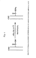
Fig. 3 shows a reaction scheme for synthesis of carbon nanotube
carboxylic acid in (Addition Step) of Example 1;
Fig. 4 shows a reaction scheme for esterification in (addition
step) of Example 1;
Fig. 5 shows a reaction scheme for cross-linking through an
ester exchange reaction in (Cross-linking Step) of Example 1;
Fig. 6A is a plan view of a silicon wafer 12 having a carbon
nanotube structure layer 14 and a resist layer formed for explaining
a shape of a portion of the resist layer 16 to remain, showing the
silicon wafer 12 seen from a side of the resist layer 16;
Fig. 6B is a plan view of a substrate seen from a side of the
resist layer on the substrate after a removal step in Example 1;
Fig. 7 is a plan view after resist removal in Example 1;
Fig. 8 is a graph showing results of measuring current-voltage
characteristics of a carbon nanotube structure layer formed in
Example 1 and a deposition layer formed in Comparative Example 1;
Fig. 9 is a schematic diagram showing an electrical switch
as an embodiment of the present invention;
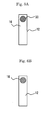
Fig. 10A is a schematic diagram showing an electrical rotary
switch as an embodiment of the present invention, which is a plan
view showing a rotary switch consisting of an insulating support
plate 17 of ceramics or the like fixed with multiple electrical
contacts 14; and
Fig. 10B is a schematic diagram showing an electrical rotary
switch as an embodiment of the present invention, showing a sectional
diagram of Fig. 10A along B-B.
Detailed Description of
the Preferred Embodiment
Hereinafter, the present invention will be specifically
described through a description of an embodiment. In the following
description, an electrical switch as an example of an electrical
device employing an electrode as an example of an electrical member
and a method of manufacturing the electrical switch are described
separately.
[Electrical Switch]
An electrical switch 60 as an example of an electrical device
of the present invention has a feature that an electrical contact
has a carbon nanotube structure having a network structure
constructed by mutually cross-linking multiple carbon nanotubes.
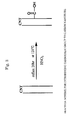
Fig. 9 shows an example of the structure of the electrical
switch 60.
In Fig. 9, the electrical switch 60 consists of: a movable
piece (first electrode) 50' including an electrical contact 14'
fixed on a base body 12'; and a fixed piece (second electrode) 50
including an electrical contact 14 fixed on a base body 12. The
electrical contacts 14 and 14' used herein each employ a carbon
nanotube structure layer described later. The movable piece 50'
moves to a direction of an arrow and to a direction opposite to
the arrow for switching on and off. That is, the movable piece 50'
is moved to the direction of an arrow by a not-shown magnet and
the electrical contact 14 is brought in contact with the electrical
contact 14', thereby connecting an electrical path between the
movable piece 50' and the fixed piece 50. On the other hand, the
movable piece 50' is moved to the direction opposite to the arrow
as in Fig. 9, thereby disconnecting the electrical path.
In the electrical switch of the embodiment of the present
invention, as described later, the electrical contact has a carbon
nanotube structure layer having a network structure constructed
by mutually cross-linking multiple carbon nanotubes. Further, the
cross-linking agent is not self-polymerizable, thereby forming a
highly dense network having uniform characteristics. Thus, the
electrical contact is hardly deteriorated through surface oxidation
and has excellent electrical conductivity, thereby improving
stability of electrical connection of the electrical switch.
A method of patterning, if required for a carbon nanotube
structure, is determined by the shape of a base body. A carbon
nanotube structure layer may be patterned directly on a base body
surface. Alternatively, a base body and a patterned carbon nanotube
structure layer carried on the base body may be attached together
onto a second base body, or the patterned carbon nanotube structure
layer alone may be transferred to the second base body.
A base body to have an electrical contact for an electrical
switch formed is not particularly limited. Metals, conductive
plastics, conductive ceramics, conductive semiconductors, or the
like can be used.
<Carbon Nanotube Structure>
In the present invention, the term "carbon nanotube structure"
refers to a structure having a network structure constructed by
mutually cross-linking multiple carbon nanotubes. Provided that
a carbon nanotube structure can be formed in such a manner that
carbon nanotubes are mutually cross-linked to construct a network
structure, the carbon nanotube structure may be formed through any
method. However, the carbon nanotube structure is preferably
manufactured through a method of manufacturing an electrical device
of the present invention described later for easy manufacture, a
high-performance electrical contact, and easy uniformization and
control of characteristics.
A first structure for the carbon nanotube structure employed
as an electrical contact manufactured through the method of
manufacturing an electrical device of the present invention
described later is manufactured by curing a solution (cross-linking
solution) containing carbon nanotubes having functional groups and
a cross-linking agent that prompts a cross-linking reaction with
the functional groups, to prompt a cross-linking reaction between
the functional groups of the carbon nanotubes and the cross-linking
agent, to thereby form a cross-linked site. Furthermore, a second
structure for the carbon nanotube structure is manufactured by
chemically bonding together functional groups of carbon nanotubes
to form cross-linked sites.
Hereinafter, the carbon nanotube structure layer in the
electrical contact for the electrical member and electrical device
of the present invention will be described by way of examples of
the manufacturing method. Unless otherwise stated, the structures
of cross-linked sites are not considered.
(Carbon Nanotube)
Carbon nanotubes, which are the main component in the present
invention, may be single-wall carbon nanotubes or multi-wall carbon
nanotubes each having two or more layers. Whether one or both types
of carbon nanotubes are used (and, if only one type is used, which
type is selected) may be decided appropriately taking into
consideration the use of the electrical member or the cost.
The carbon nanotube structure layer employed as an electrical
contact preferably contains a multi-wall carbon nanotube (MWNT)
for each of the multiple carbon nanotubes in the layer, for suppressing
resistance loss due to wiring. An electrically conductive
single-wall carbon nanotube (SWNT) can also be used, but SWNT is
manufactured as a mixture of semiconductive and conductive carbon
nanotubes and extraction of the conductive carbon nanotubes is
difficult. Thus, MSNT mainly containing conductive carbon
nanotubes is preferably used for the carbon nanotube structure layer
to serve as an electrical contact.
Carbon nanotubes in the present invention include ones that
are not exactly shaped like a tube, such as: a carbon nanohorn (a
horn-shaped carbon nanotube whose diameter continuously increases
from one end toward the other end) which is a variant of a single-wall
carbon nanotube; a carbon nanocoil (a coil-shaped carbon nanotube
forming a spiral when viewed in entirety); a carbon nanobead (a
spherical bead made of amorphous carbon or the like with its center
pierced by a tube); a cup-stacked nanotube; and a carbon nanotube
with its outer periphery covered with a carbon nanohorn or amorphous
carbon.
Furthermore, carbon nanotubes in the present invention may
include ones that contain some substances inside, such as: a
metal-containing nanotube which is a carbon nanotube containing
metal or the like; and a peapod nanotube which is a carbon nanotube
containing a fullerene or a metal-containing fullerene.
As described above, in the present invention, it is possible
to employ carbon nanotubes of any form, including common carbon
nanotubes, variants of the common carbon nanotubes, and carbon
nanotubes with various modifications, without a problem in terms
of reactivity. Therefore, the concept of "carbon nanotube" in the
present invention encompasses all of the above.
Those carbon nanotubes are conventionally synthesized through
a known method such as arc discharge, laser ablation, or CVD, and
the present invention can employ any of the methods. However, arc
discharge in a magnetic field is preferable from the viewpoint of
synthesizing a highly pure carbon nanotube.
A diameter of carbon nanotubes used in the present invention
is preferably 0.3 nm or more and 100 nm or less. A diameter of the
carbon nanotubes exceeding this upper limit undesirably results
in difficult and costly synthesis. A more preferable upper limit
of the diameter of a carbon nanotubes is 30 nm or less.
In general, the lower limit of the carbon nanotube diameter
is about 0.3 nm from a structural standpoint. However, too small
a diameter could undesirably lower the synthesis yield. It is
therefore preferable to set the lower limit of the carbon nanotube
diameter to 1 nm or more, more preferably 10 nm or more.
The length of carbon nanotubes used in the present invention
is preferably 0.1 µm or more and 100 µm or less. A length of the
carbon nanotubes exceeding this upper limit undesirably results
in difficult synthesis or requires a special synthesis method raising
cost. On the other hand, a length of the carbon nanotubes falling
short of this lower limit undesirably reduces the number of cross-link
bonding points per carbon nanotube. A more preferable upper limit
of the carbon nanotube length is 10 µm or less, and a more preferable
lower limit of the carbon nanotube length is 1 µm or more.
The appropriate carbon nanotube content in the cross-linking
solution varies depending on the length and thickness of carbon
nanotubes, whether single-wall carbon nanotubes or multi-wall carbon
nanotubes are used, the type and amount of functional groups in
the carbon nanotubes, the type and amount of cross-linking agent
or of an additive for bonding functional groups together, the presence
or absence of a solvent or other additive used and, if one is used,
the type and amount of the solvent or additive, etc. The carbon
nanotube content in the solution should be high enough to form a
satisfactory carbon nanotube structure after curing but not
excessively high because the applicability deteriorates.
Specifically, the ratio of carbon nanotubes to the entire
cross-linking solution excluding the mass of the functional groups
is 0.01 to 10 g/l, preferably 0.1 to 5 g/l, and more preferably
0.5 to 1.5 g/l, although the ranges cannot be determined uniquely
if the parameters are different as described above.
The purity of the carbon nanotubes to be used is desirably
raised by purifying the carbon nanotubes before preparation of the
cross-linking solution if the purity is not high enough. In the
present invention, the higher the carbon nanotube purity, the better
the result can be. Specifically, the purity is preferably 90% or
higher, more preferably 95% or higher. Low purity causes the
cross-linking agent to cross-link with carbon products such as
amorphous carbon and tar, which are impurities. This could change
the cross-linking distance between carbon nanotubes, and desired
characteristics may not be obtained. A purification method for
carbon nanotubes is not particularly limited, and any known
purification method can be employed.
Such carbon nanotubes are used for the formation of a carbon
nanotube structure with predetermined functional groups added to
the carbon nanotubes. A preferable functional group to be added
at this time varies depending on whether the carbon nanotube structure
is formed through the first method or second method described above
(a preferable functional group in the former case is referred to
as "functional group 1", and a preferable functional group in the
latter case is referred to as "functional group 2").
How functional groups are introduced into carbon nanotubes
will be described in the section below titled (Method of Preparing
Cross-linking Solution).
Hereinafter, components that can be used for the formation
of a carbon nanotube structure will be described for the respective
first and second methods.
(Case of First Method)
In the first method in which a cross-linked site is formed
using a cross-linking agent, carbon nanotubes can have any functional
group to be connected thereto without particular limitations, as
long as functional groups selected can be added to the carbon nanotubes
chemically and can prompt a cross-linking reaction with any type
ofcross-linkingagent. Specific examples of such functional groups
include -COOR, -COX, -MgX, -X (where X represents halogen), -OR,
-NR1R2, -NCO, -NCS, -COOH, -OH, -NH2, -SH, -SO3H, -R"CH2OH, -CHO,
-CN, -COSH, -SR, -SiR'3 (In the above formulae, R, R1, R2, R', and
R" each independently represent a substituted or unsubstituted
hydrocarbon group. R, R1, R2, and R' are each a monovalent hydrocarbon
group and are each preferably independently selected from -CnH2n-1
and -CnH2n+1 (n represents an integer of 1 to 10).. Of those, a methyl
group or an ethyl group is more preferable for each of R, R1, R2,
and R'. R" is a divalent hydrocarbon group and is preferably
selected from -CnH2n- (n represents an integer of 1 to 10). Of those,
a methylene group or an ethylene group is more preferable for R' ' . ) .
Note that the functional groups are not limited to those examples.
Of those, it is preferable to select at least one functional
group from the group consisting of -OH, -COOH, -COOR (In the formulae,
R represents a substituted or unsubstituted hydrocarbon group. R
is preferably selected from -CnH2n-1 and -CnH2n+1 (n represents an
integer of 1 to 10). Of those, a methyl group or an ethyl group
is more preferable.), -COX (where X represents a halogen atom),
-NH2, and -NCO. In that case, a cross-linking agent, which can prompt
a cross-linking reaction with the selected functional group, is
selected as the cross-linking agent.
In particular, -COOR (R is the same as that described above)
is particularly preferable. This is because a carboxyl group can
be introduced into a carbon nanotube with relative ease, because
the resultant substance (carbon nanotube carboxylic acid) can be
easily introduced as a functional group by esterifying the substance,
and because the substance has good reactivity with a cross-linking
agent.
R in the functional group -COOR is a substituted or
unsubstituted hydrocarbon group, and is not particularly limited.
However, R is preferably an alkyl group having 1 to 10 carbon atoms,
more preferably an alkyl group having 1 to 5 carbon atoms, and
particularly preferably a methyl group or an ethyl group in terms
of reactivity, solubility, viscosity, and ease of use as a solvent
for a cross-linking solution.
The amount of functional groups introduced cannot be determined
uniquely because the amount varies depending on the length and
thickness of a carbon nanotube, whether the carbon nanotube is of
a single-wall type or a multi-wall type, the type of a functional
group, the use of the electrical member, etc. From the viewpoint
of the strength of the cross-linked substance obtained, namely,
the strength of the carbon nanotube structure, a preferable amount
of functional groups introduced is large enough to add two or more
functional groups to each carbon nanotube. How functional groups
are introduced into carbon nanotubes will be described in the section
below titled [Method of Manufacturing Electrical Device].
(Cross-linking Agent)
A cross-linking agent is an essential ingredient for the
cross-linking solution. Any cross-linking agent can be used as long
as the cross-linking agent is capable of prompting a cross-linking
reaction with the functional groups of the carbon nanotubes. In
other words, the type of cross-linking agent that can be selected
is limited to a certain degree by the types of the functional groups.
Also, the conditions of curing (heating, UV irradiation, visible
light irradiation, air setting, etc. ) as a result of the cross-linking
reaction are naturally determined by the combination of those
parameters.
Specific examples of the preferable cross-linking agent
include a polyol, a polyamine, a polycarboxylic acid, a
polycarboxylate, apolycarboxylic acid halide, apolycarbodiimide,
and a polyisocyanate. It is preferable to select at least one
cross-lining agent from the group consisting of the above
cross-linking agents. In that case, a functional group which can
prompt a reaction with the cross-linking agent is selected as the
functional group.
At least one functional group and at least one cross-linking
agent are particularly preferably selected respectively from the
group consisting of the functional groups exemplified as the
preferable functional groups and the group consisting of the
cross-linking agents exemplified as the preferable cross-linking
agents, so that a combination of the functional group and the
cross-linking agent may prompt a cross-linking reaction with each
other. The following Table 1 lists the combinations of the functional
group of the carbon nanotubes and the corresponding cross-linking
agent, which can prompt a cross-linking reaction, along with curing
conditions of the combinations.
| Functional group of carbon nanotube | Cross-linking agent | Curing condition |
| -COOR | Polyol | heat curing |
| -COX | Polyol | heat curing |
| -COOH | Polyamine | heat curing |
| -COX | Polyamine | heat curing |
| -OH | Polycarboxylate | heat curing |
| -OH | Polycarboxylic acid halide | heat curing |
| -NH2 | Polycarboxylic acid | heat curing |
| -NH2 | Polycarboxylic acid halide | heat curing |
| -COOH | Polycarbodiimide | heat curing |
| -OH | Polycarbodiimide | heat curing |
| -NH2 | Polycarbodiimide | heat curing |
| -NCO | Polyol | heat curing |
| -OH | Polyisocyanate | heat curing |
| -COOH | Ammonium complex | heat curing |
| -COOH | Hydroquinone | heat curing |
| *where R represents a substituted or unsubstituted hydrocarbon group |
| *where X represents a halogen |
Of those combinations, preferable is the combination of -COOR
(R represents a substituted or unsubstituted hydrocarbon group.
R is preferably selected from -CnH2n-1 and -CnH2n+1 (n represents an
integer of 1 to 10). Of those, a methyl group or an ethyl group
is more preferable.) with good reactivity on a functional group
side and a polyol, which form a robust cross-linked substance with
ease. The term "polyol" in the present invention is a genetic name
for organic compounds each having two or more OH groups. Of those,
one having 2 to 10 (more preferably 2 to 5) carbon atoms and 2 to
22 (more preferably 2 to 5) OH groups is preferable in terms of
cross-linkability, solvent compatibility when an excessive amount
thereof is charged, treatability of waste liquid after a reaction
by virtue of biodegradability (environmental suitability), yield
of polyol synthesis, and so on. In particular, the number of carbon
atoms is preferably lower within the above range because a gap between
carbon nanotubes in the resultant carbon nanotube structure can
be narrowed to bring the carbon nanotubes into substantial contact
with each other (to bring the carbon nanotubes close to each other).
Specifically, glycerin and ethylene glycol are particularly
preferable, and one or both of glycerin and ethylene glycol are
preferably used as a cross-linking agent.
From another perspective, the cross-linking agent is
preferably a not self-polymerizable cross-linking agent. In
addition to glycerin and ethylene glycol as examples of the polyols,
butenediol, hexynediol, hydroquinone, and naphthalenediol are
obviously not self-polymerizable cross-linking agents. More
generally, a prerequisite for the not self-polymerizable
cross-linking agent is to be without a pair of functional groups,
which can prompt a polymerization reaction with each other, in itself .
On the other hand, examples of a self-polymerizable cross-linking
agent include one that has a pair of functional groups, which can
prompt a polymerization reaction with each other (alkoxide, for
example), in itself.
According to a method of manufacturing an electrical member
and electrical device of the present invention, the first method
may involve: further including a solvent in the solution used in
the supplying step and containing the multiple carbon nanotubes
to which the functional groups are bonded and the cross-linking
agent; and supplying the base body surface with the resultant solution.
The cross-linking agent may also serve as the solvent depending
on type of the cross-linking agent.
Formation of a carbon nanotube structure only involves:
supplying the base body surface with the multiple carbon nanotubes
to which functional groups are bonded and the cross-linking agent
(the supplying step in the method of manufacturing an electrical
member or electrical device of the present invention) ; and chemically
bonding the functional groups together to form a cross-linked site
(the cross-linking step in the method of manufacturing an electrical
member or electrical device of the present invention). In supplying
the base body surface with the multiple carbon nanotubes to which
functional groups are bonded and the cross-linking agent, the base
body surface is preferably supplied with a solution (cross-linking
solution) containing the carbon nanotubes, the cross-linking agent,
and a solvent. In particular, the solution is applied as a
cross-linking application liquid to form a cross-linked substance
film, for a simple, low cost operation in a short period of time.
(Case of second method)
In the second method in which a cross-linked site of a carbon
nanotube structure is formed by mutually cross-linking multiple
functional groups bonded to carbon nanotubes each having at least
one end different through chemical bonding of the functional groups,
to thereby construct a network structure. The functional group to
be bonded to the carbon nanotubes is not particularly limited as
long as the functional group can be chemically added to the carbon
nanotubes and is capable of reacting with each other using any type
of additive. Specific examples of the functional group include -COOR,
-COX, -MgX, -X (where X represents a halogen), -OR, -NR1R2, -NCO,
-NCS, -COOH, -OH, -NH2, -SH, -SO3H, -R''CH2OH, -CHO, -CN, -COSH,
-SR, -SiR'3 (In the above formulae, R, R1, R2, R', and R" each
independently represent a substituted or unsubstituted hydrocarbon
group. R, R1, R2, and R' are each a monovalent hydrocarbon group
and are preferably independently selected from -CnH2n-1 and -CnH2n+1
(n represents an integer of 1 to 10). Of those, a methyl group or
an ethyl group is more preferable for each of R, R1, R2, and R'.
R'' is a divalent hydrocarbon group and is preferably selected from
-CnH2n- (n represents an integer of 1 to 10) . Of those, a methylene
group or an ethylene group is more preferable for R''.). However,
the functional group is not limited to those.
A reaction for chemically bonding the functional groups
together is particularly preferably dehydration condensation, a
substitution reaction, an addition reaction, or an oxidative
reaction. The functional groups preferable for the respective
reactions out of the above functional groups are exemplified below.
According to a method of manufacturing an electrical member
and electrical device of the present invention, the second method
may involve: preparing a supply solution (cross-linking solution)
used in the supplying step by including the multiple carbon nanotubes
having the functional groups bonded and the additive as required
in a solvent; and supplying the base body surface with the resultant
solution.
When the reaction for chemically bonding the functional groups
together is dehydration condensation, a condensation agent is
preferably added as the additive. Specific examples of preferable
condensation agents include an acid catalyst and a dehydration
condensation agent such as sulfuric acid,
N-ethyl-N'-(3-dimethylaminopropyl)carbodiimide, and dicyclohexyl
carbodiimide. It is preferable to select at least one condensation
agent from the group consisting of the above. In that case, the
functional groups, which can prompt a reaction among the functional
groups with the help of the selected condensation agent, are selected
as the functional groups.
The functional groups to be used in dehydration condensation
are preferably at least one functional group selected from the group
consisting of -COOR (R represents a substituted or unsubstituted
hydrocarbon group and is preferably selected from -CnH2n-1 and -CnH2n+1
(n represents an integer of 1 to 10) . Of those, a methyl group or
an ethyl group is more preferable.), -COOH, -COX (where X represents
a halogen atom), -OH, -CHO, and -NH2.
Examples of the functional group particularly preferable for
use in dehydration condensation include -COOH. Introduction of a
carboxyl group into carbon nanotubes is relatively easy, and the
resultant substance (carbon nanotube carboxylic acid) has high
reactivity. Therefore, functional groups for forming a network
structure can be easily introduced into multiple sites of one carbon
nanotube. Moreover, the functional group is suitable for formation
of a carbon nanotube structure because the functional group is easily
subjected to dehydration condensation. If the functional group to
be used in dehydration condensation is -COOH, sulfuric acid,
N-ethyl-N'-(3-dimethylaminopropyl)carbodiimide, and dicyclohexyl
carbodiimide described above are particularly preferable
condensation agents.
When the reaction for chemically bonding the functional groups
together is a substitution reaction, a base is preferably added
astheadditive. A base that can be added is not particularly limited,
and may be any base as long as the base is selected depending on
the acidity of a hydroxyl group.
Specific preferable examples of the base include sodium
hydroxide, potassium hydroxide, pyridine, and sodium ethoxide. It
is preferable to select at least one base from the group consisting
of the above bases. In that case, functional groups, which can prompt
a substitution reaction among the functional groups with the help
of the selected base, are selected as the functional groups. In
addition, the functional groups at this time are preferably at least
one functional group selected from the group consisting of -NH2,
-X (where X represents a halogen atom), -SH, -OH, -OSO2CH3, and
-OSO2(C6H4)CH3.
When the reaction for chemically bonding the functional groups
together is an addition reaction, anadditive is not always necessary.
The functional groups at this time are preferably -OH and/or -NCO.
When the reaction for chemically bonding the functional groups
together is an oxidative reaction, an additive is not always necessary
either. However, an oxidative reaction accelerator is preferably
added as the additive. An example of the oxidative reaction
accelerator that can be suitably added is iodine. In addition, the
functional groups at this time are preferably -SH.
Further, it is also possible to bond a molecule, which partially
contains those functional groups, with the carbon nanotubes to be
chemically bonded at a preferable functional group portion
exemplified above. Even in this case, a functional group with a
large molecular weight to be bonded to the carbon nanotubes is bonded
as intended, enabling control of a length of the cross-linked site.
In chemically bonding the functional groups together, an
additive that can form the chemical bonding among the functional
groups can be used. Any additive that is capable of causing the
functional groups of the carbon nanotubes to react with each other
can be used as such an additive. In other words, the type of additive
that can be selected is limited to a certain degree by the types
of the functional groups and the reaction. Also, the condition of
curing (heating, UV irradiation, visible light irradiation, air
setting, etc.) as a result of the reaction is naturally determined
by the combination of those parameters.
It is preferable to select at least two functional groups from
the group consisting of the functional groups exemplified as
preferable functional groups so that a combination of the selected
functional groups is capable of prompting a mutual reaction. Table
2 below lists functional groups (A) and (B) of carbon nanotubes
capable of prompting a mutual cross-linking reaction and the names
of corresponding reactions.
| Cross-linked site | Functional group of carbon nanotube(A) | Functional group of carbon nanotube (B) | Reaction |
| -COOCO- | -COOH | - | Dehydration condensation |
| -S-S- | -SH | - | Oxidative reaction |
| -O- | -OH | - | Dehydration condensation |
| -NH-CO- | -COOH | - NH2 | Dehydration condensation |
| -COO- | -COOH | -OH | Dehydration condensation |
| -COO- | -COOR | -OH | Dehydration condensation |
| -COO- | -COX | -OH | Dehydration condensation |
| -CH=N- | -CHO | -NH2 | Dehydration condensation |
| -NH- | -NH2 | -X | reaction |
| -S- | -SH | -X | Substitution reaction |
| -O- | -OH | -X | Substitution reaction |
| -O- | -OH | -OSO2CH3 | Substitution reaction |
| -O- | -OH | -OSO2(C6H4)CH3 | Substitution reaction |
| -NH-COO- | -OH | -N=C=O | Addition reaction |
| *where R represents a substituted or unsubstituted hydrocarbon group |
| *where X represents a halogen |
Formation of a carbon nanotube structure only involves:
supplying the base body surface with the multiple carbon nanotubes
to which functional groups are bonded and the additive as required
(supplying step in the method of manufacturing an electrical member
or electrical device of the present invention); and chemically
bonding the functional groups together to form a cross-linked site
(cross-linking step in the method of manufacturing an electrical
member or electrical device of the present invention). In supplying
the base body surface with the multiple carbon nanotubes to which
functional groups are bonded, the base body surface is preferably
supplied with a solution (cross-linking solution) containing the
carbon nanotubes and a solvent. In particular, the solution is
applied as a cross-linking application liquid to form a cross-linked
substance film, for simple formation of the electrical member or
electrical device of the present invention at a low cost and in
a short period of time.
(Other Additive)
The cross-linking solution (included in both the first method
and the second method) may contain various additives including a
solvent, a viscosity modifier, a dispersant, and a cross-linking
accelerator. A solvent is added when satisfactory applicability
of the cross-linking solution is not achieved with solely the
cross-linking agent or the additive for bonding the functional groups.
A solvent that can be employed is not particularly limited, and
may be appropriately selected according to the type of the
cross-linking agent or the additive forbonding the functional groups.
Specific examples of such a solvent include: organic solvents such
as methanol, ethanol, isopropanol, n-propanol, butanol, methyl ethyl
ketone, toluene, benzene, acetone, chloroform, methylene chloride,
acetonitrile, diethyl ether, and tetrahydrofuran (THF); water;
acidic aqueous solutions; and alkaline aqueous solutions. A solvent
as such is added in an amount that is not particularly limited but
determined appropriately by taking into consideration the
applicability of the cross-linking solution.
A viscosity modifier is added when sufficient applicability
is not achieved with solely the cross-linking agent or the additive
for bonding the functional groups. A viscosity modifier that can
be employed is not particularly limited, and may be appropriately
selected according to the type of cross-linking agent or the additive
for bonding the functional groups. Specific examples of such a
viscosity modifier include methanol, ethanol, isopropanol,
n-propanol, butanol, methyl ethyl ketone, toluene, benzene, acetone,
chloroform, methylene chloride, acetonitrile, diethyl ether, and
THF.
Some of those viscosity modifiers serve as a solvent when added
in a certain amount, but it is meaningless to clearly distinguish
the viscosity modifier from the solvent. A viscosity modifier as
such is added in an amount that is not particularly limited but
determined appropriately by taking into consideration the
applicability.
A dispersant is added in order to maintain the dispersion
stability of the carbon nanotubes, the cross-linking agent, or the
additive for bonding the functional groups in the cross-linking
solution. Various known surfactants, water-soluble organic
solvents, water, acidic aqueous solutions, alkaline aqueous
solutions, etc. can be employed as a dispersant. However, a
dispersant is not always necessary since components themselves of
the cross-linking solution have high dispersion stability. In
addition, depending on the use of the final electrical member, the
presence of impurities such as a dispersant in the carbon nanotube
structure may not be desirable. In such a case, a dispersant is
not added at all, or is added in a very small amount.
The content of the cross-linking agent or additive for bonding
the functional groups in the cross-linking solution varies depending
on the type of cross-linking agent (including whether the
cross-linking agent is self-polymerizable or not
self-polymerizable) or additive for bonding functional groups. The
content also varies depending on the length and thickness of carbon
nanotubes, whether single-wall carbon nanotubes ormulti-wall carbon
nanotubes are used, the type and amount of functional groups in
the carbon nanotubes, the presence or absence of a solvent or other
additive used and, if one is used, the type and amount of the solvent
or additive, etc. Therefore, the content cannot be determined
uniquely. In particular, for example, glycerin or ethylene glycol
can also provide characteristics of a solvent because a viscosity
of glycerin or ethylene glycol is not so high, and thus an excessive
amount of glycerin or ethylene glycol can be added.
<Method of Preparing Cross-linking Solution>
A method of preparing a cross-linking solution is described
next. The cross-linking solution is prepared by mixing carbon
nanotubes that have functional groups with a cross-linking agent
or an additive for bonding functional groups that prompts a
cross-linking reaction with the functional groups (mixing step).
The mixing step may be preceded by an addition step in which the
functional groups are introduced into the carbon nanotubes.
Use of carbon nanotubes having functional groups as starting
materials starts the preparation from the mixing step. The use of
normal carbon nanotubes themselves as starting materials starts
the preparation from the addition step.
(Addition Step)
The addition step is a step of introducing desired functional
groups into carbonnanotubes. How functional groups are introduced
varies depending on the type of functional group and cannot be
determined uniquely. One method involves adding a desired
functional group directly. Another method involves: introducing
a functional group that is easily added; and then substituting the
whole functional group or a part thereof, or adding a different
functional group to the former functional group, in order to obtain
the target functional group.
Still another method involves applying a mechanochemical force
to a carbon nanotube to break or modify a very small portion of
a graphene sheet on the surface of the carbon nanotube, to thereby
introduce various functional groups into the broken or modified
portion.
Furthermore, functional groups can be relatively easily
introduced into cup-stacked carbon nanotubes, which have many
defects on the surface upon manufacture, and carbon nanotubes that
are formed by vapor phase growth. On the other hand, carbon nanotubes
each having a perfect graphene sheet structure exert the carbon
nanotube characteristics more effectively and the characteristics
are easily controlled. Consequently, it is particularly preferable
to use a multi-wall carbon nanotube so that an appropriate number
of defects are formed on its outermost layer as electrical contacts
to bond functional groups for cross-linking while the inner layers
having less structural defects exert the carbon nanotube
characteristics.
Operations for the addition step are not particularly limited,
and any known method can be employed. Various addition methods
disclosed in JP 2002-503204 A may be employed in the present invention
depending on the purpose.
A description is given on a method of introducing -COOR (In
the formula, R represents a substituted or unsubstituted hydrocarbon
group. R is preferably selected from -CnH2n-1 and -CnH2n+1 (n represents
an integer of 1 to 10) . Of those, a methyl group or an ethyl group
is more preferable.), a particularly desirable functional group
among the functional groups listed above. To introduce -COOR (where
R represents a substituted or unsubstituted hydrocarbon group) into
carbon nanotubes, carboxyl groups may be (1) added to the carbon
nanotubes once, and then (2) esterified.
(1) Addition of Carboxyl Group
To introduce carboxyl groups into carbon nanotubes, carboxyl
groups are refluxed together with an acid having an oxidizing effect.
This operation is relatively easy and is preferable since carboxyl
groups with high reactivity can be added to carbon nanotubes. A
brief description of the operation is given below.
Examples of an acid having an oxidizing effect include
concentrated nitric acid, a hydrogen peroxide solution, a mixture
ofsulfuricacidandnitricacid,andaquaregia. Concentratednitric
acid is particularly used in concentration of preferably 5 mass%
or higher, more preferably 60 mass% or higher.
Anormalrefluxmethodcanbeemployed. Therefluxtemperature
is preferably close to the boiling point of the acid used. When
concentrated nitric acid is used, for instance, the temperature
is preferably set to 120 to 130 °C. The reflux preferably lasts for
30 minutes to 20 hours, more preferably for 1 hour to 8 hours.
Carbon nanotubes to which carboxyl groups are added (carbon
nanotube carboxylic acid) are produced in the reaction liquid after
the reflux. The reaction liquid is cooled down to room temperature
and then is subj ected to a separation operation or washing as required,
thereby obtaining the target carbon nanotube carboxylic acid.
(2) Esterification
The target functional group -COOR (where R represents a
substituted or unsubstituted hydrocarbon group and a preferable
R is such as that described above) can be introduced by adding an
alcohol to the obtained carbon nanotube carboxylic acid and
dehydrating the mixture for esterification.
The alcohol used for the esterification is determined according
to R in the formula of the functional group. That is, if R is CH3,
the alcohol is methanol, and if R is C2H5, the alcohol is ethanol.
A catalyst is generally used in the esterification, and a
conventionally known catalyst such as sulfuric acid, hydrochloric
acid, or toluenesulfonic acid can be used in the present invention.
The use of sulfuric acid as a catalyst is preferable from the viewpoint
of not prompting a side reaction in the present invention.
The esterification may be conducted by adding an alcohol and
a catalyst to carbon nanotube carboxylic acid and refluxing the
mixture at an appropriate temperature for an appropriate time period.
A temperature condition and a time period condition in this case
depend on type of catalyst, type of alcohol, or the like and cannot
be determined uniquely, but a reflux temperature is preferably close
to the boiling point of the alcohol used. The reflux temperature
is preferably in the range of 60 to 70°C for methanol, for example.
Further, a reflux time period is preferably in the range of 1 to
20 hours, more preferably in the range of 4 to 6 hours.
A carbon nanotube with the functional group -COOR (where R
represents a substituted or unsubstituted hydrocarbon group and
a preferable R is such as that described above) added can be obtained
by separating a reaction product from a reaction liquid after
esterification and washing the reaction product as required.
(Mixing Step)
The mixing step is a step of mixing, as required, carbon
nanotubes having functional groups with a cross-linking agent
prompting a cross-linking reaction with the functional groups or
an additive for bonding the functional groups, to thereby prepare
the cross-linking solution. In the mixing step, other components
described in the aforementioned section titled [Electrical Switch]
are mixed, in addition to the carbon nanotubes having functional
groups and the cross-linking agent. Then, an amount of a solvent
or a viscosity modifier is preferably adjusted considering
applicability, to thereby prepare the cross-linking solution
(cross-linking application liquid) just before supply (application)
to the base body.
Simple stirring with a spatula and stirring with a stirrer
of a stirring blade type, a magnetic stirrer, and a stirring pump
may be used. However, to achieve higher degree of uniformity in
dispersion of the carbon nanotubes to enhance storage stability
while fully extending a network structure by cross-linking of the
carbon nanotubes, an ultrasonic disperser or a homogenizer may be
used for powerful dispersion. However, the use of a stirring device
with a strong shear force of stirring such as a homogenizer may
cut or damage the carbon nanotubes in the solution, thus the device
may be used for a very short period of time.
A carbon nanotube structure is formed by supplying the base
body surface with the cross-linking solution described above and
curing the cross-linking solution. A supplying method and a curing
method are described in detail in the section below titled [Method
of Manufacturing Electrical Device].
The carbon nanotube structure in the present invention is in
a state in which carbon nanotubes are networked. In detail, the
carbon nanotube structure is cured into a matrix form in which carbon
nanotubes are connected to each other through cross-linked sites,
thereby sufficiently exerting the characteristics of a carbon
nanotube itself such as high electron- and hole-transmission
characteristics. In other words, the carbon nanotube structure
layer has carbon nanotubes that are tightly connected to each other,
contains no other binders and the like, and is thus composed
substantially only of carbon nanotubes, so that characteristics
peculiar to a carbon nanotube are used fully.
A thickness of the carbon nanotube structure layer of the
present invention can be widely selected from being very thin to
being thick according to an application. Lowering a content of the
carbon nanotubes in the cross-linking solution used (simply,
lowering the viscosity by diluting) and applying the cross-linking
solution as a thin film provide a very thin coat. Similarly, raising
a content of the carbon nanotubes provides a thick coat. Further,
repeating the application provides an even thicker coat. A very
thin coat from a thickness of about 10 nm can be formed, and a thick
coat without an upper limit can be formed through recoating. A
possible film thickness with one coating is about 5 µm. Further,
a coat may have a desired shape by pouring the cross-linking solution
having a content or the like adjusted into a mold and bonding.
In forming the carbon nanotube structure according to the first
method, a site where the carbon nanotubes are mutually cross-linked,
that is, the cross-linked site formed through a cross-linking
reaction between the functional groups of the carbon nanotubes and
the cross-linking agent has a cross-linking structure. In the
cross-linking structure, residues of the functional groups remaining
after the cross-linking reaction are connected together with a
connecting group, which is a residue of the cross-linking agent
remaining after the cross-linking reaction.
As described, the cross-linking agent, which is a component
of the cross-linking solution, is preferably not self-polymerizable.
A not self-polymerizable cross-linking agent provides the finally
formed carbon nanotube structure constructed from a residue of only
one cross-linking agent. The gap between the carbon nanotubes to
be cross-linked can be controlled to a size of a residue of the
cross-linking agent used, thereby providing a desired network
structureofthecarbonnanotubeswithhighduplicability. Further,
multiple cross-linking agents are not present between the carbon
nanotubes, thus enabling enhancement of an actual density of the
carbon nanotubes in the carbon nanotube structure. Further,
reducing a size of a residue of the cross-linking agent can extremely
narrow a gap between each of the carbon nanotubes both electrically
and physically (carbon nanotubes are substantially in direct contact
with each other).
Formation of the carbon nanotube structure layer with a
cross-linking solution prepared by selecting a single functional
group of the carbon nanotubes and a single not self-polymerizable
cross-linking agent results in the cross-linked site of the layer
having an identical cross-linking structure (Example 1). Further,
formation of the carbon nanotube structure layer with a cross-linking
solution prepared by selecting even multiple types of functional
groups of the carbon nanotubes and/or multiple types of not
self-polymerizable cross-linking agents results in the cross-linked
sites of the layer mainly having a cross-linking structure based
on a combination of the functional group and the not
self-polymerizable cross-linking agent mainly used (Example 2).
In contrast, formation of the carbon nanotube structure layer
with a cross-linking solution prepared by selecting
self-polymerizable cross-linking agents, without regard to whether
the functional groups of the carbon nanotubes and the cross-linking
agents are of single or multiple types, results in the cross-linked
sites in the carbon nanotube structure where carbon nanotubes are
cross-linked together without a main, specific cross-linking
structure. This is because the cross-linked sites will be in a state
where numerous connecting groups with different connecting
(polymerization) numbers of the cross-linking agents coexist.
In other words, by selecting not self-polymerizable
cross-linking agents, the cross-linked sites, where the carbon
nanotubes of the carbon nanotube structure cross-link together,
have a mainly identical cross-linking structure because a residue
of only one cross-linking agent bonds with the functional groups.
"Mainly identical" here is a concept including a case where all
of the cross-linked sites have an identical cross-linking structure
as described above (Example 1), as well as a case where the
cross-linking structure based on a combination of the functional
group and the not self-polymerizable cross-linking agent mainly
used becomes a main structure with respect to the total cross-linked
sites as described above (Example 2).
When referring to "mainly identical", a "ratio of identical
cross-linked sites" with respect to the total cross-linked sites
will not have a uniform lower limit defined. The reason is that
a case of giving a functional group or a cross-linking structure
with an aim different from formation of a carbon nanotube network
may be assumed, for example. However, in order to actualize high
electrical or physical characteristics peculiar to carbon nanotubes
with a strong network, a "ratio of identical cross-linked sites"
with respect to the total cross-linked sites is preferably 50% or
more, more preferably 70% or more, further more preferably 90% or
more, and most preferably 100%, based on numbers . Thosenumberratios
can be determined through, for example, a method of measuring an
intensity ratio of an absorption spectrum corresponding to the
cross-linking structure with an infrared spectrum.
As described, a carbon nanotube structure layer having the
cross-linked site with a mainly identical cross-linking structure
where carbon nanotubes cross-link together allows formation of a
uniform network of the carbon nanotubes in a desired state. In
addition, the carbon nanotube network can be constructed with
homogeneous, satisfactory, and expected electrical or physical
characteristics and high duplicability.
Further, the connecting group preferably contains hydrocarbon
as a skeleton thereof. "Hydrocarbon as a skeleton" here refers to
a main chain portion of the connecting group consisting of hydrocarbon,
the main portion of the connecting group contributing to connecting
together residues of the functional groups of carbon nanotubes to
be cross-linked remaining after a cross-linking reaction. A side
chain portion, where hydrogen of the main chain portion is substituted
by another substituent, is not considered. Obviously, it is more
preferable that the whole connecting group consists of hydrocarbon.
The hydrocarbon preferably has 2 to 10 carbon atoms, more
preferably 2 to 5 carbon atoms, and further more preferably 2 to
3 carbon atoms. The connecting group is not particularly limited
as long as the connecting group is divalent or more.
In the cross-linking reaction of the functional group -COOR
(where R represents a substituted or unsubstituted hydrocarbon group,
and a preferable R is such as that described above) and ethylene
glycol, exemplified as a preferable combination of the functional
group of carbon nanotubes and the cross-linking agent, the
cross-linked site where multiple carbon nanotubes are mutually
cross-linked becomes -COO(CH2)2OCO-.
Further, in the cross-linking reaction of the functional group
-COOR (where R represents a substituted or unsubstituted hydrocarbon
group, and a preferable R is such as that described above) and glycerin,
the cross-linked site where multiple carbon nanotubes are mutually
cross-linked becomes -COOCH2CHOHCH2OCO- or -COOCH2CH(OCO-)CH2OH if
two OH groups contribute to the cross-linking, and the cross-linked
site becomes -COOCH2CH(OCO-)CH2OCO- if three OH groups contribute
to the cross-linking.
As has been described, the carbon nanotube structure formed
through the first method has a network structure composed of multiple
carbon nanotubes connected to each other through multiple
cross-linked sites. Thus, contact or arrangement of carbon
nanotubes remains stable, unlike a mere carbon nanotube dispersion
film. Therefore, the carbon nanotube structure stably exerts
characteristics peculiar to carbon nanotubes including: electrical
characteristics such as high electron- or hole- transmission
characteristics; physical characteristics such as thermal
conductivity and toughness; and light absorption characteristics.
On the other hand, in forming the carbon nanotube structure
through the second method, a site where the multiple carbon nanotubes
are mutually cross-linked, that is, a cross-linked site formed by
a cross-linking reaction among the functional groups of the multiple
carbon nanotubes has a cross-linking structure in which residues
of the functional groups remaining after a cross-linking reaction
are connected to each other. In this case as well, the carbon nanotube
structure has carbon nanotubes connected to each other through a
cross-linked site in a matrix form, thereby easily exerting the
characteristics of carbon nanotubes itself such as high electron-
and hole- transmission characteristics. That is, the carbon
nanotube structure has carbon nanotubes that are tightly connected
to each other, contains no other binders and the like, and is thus
composed substantially only of carbon nanotubes.
Further, the cross-linked sites are formed through directly
reacting the functional groups, thus enabling enhancement of the
actual density of the carbon nanotubes of the carbon nanotube
structure. Further, reducing a size of a functional group can
extremely narrow a gap between each of the carbon nanotubes both
electrically and physically, thereby easily exerting the
characteristics of the carbon nanotube itself.
Further, cross-linked sites are formed by chemical bonding
of the functional groups together, and thus, the carbon nanotube
structure has a mainly identical cross-linking structure.
Therefore, a uniform network of carbon nanotubes can be formed into
a desired state. Further, the carbon nanotube structure can be
constructed with homogeneous, satisfactory, and expected electrical
and physical characteristics and high duplicability.
A layer in addition to the carbon nanotube structure may be
formed in the electrical member of the present invention. For example,
placing an adhesive layer between the base body surface and the
carbon nanotube structure for enhancing adhesiveness therebetween
is preferable for improving the adhesive strength of the carbon
nanotube structure. A method of forming an adhesive layer and other
details will be explained in the section titled [Method of
Manufacturing Electrical Device].
As has been described, the electrical contact employed in the
electrical switch in an embodiment of the present invention includes
a carbon nanotube structure having a network structure composed
of multiple carbon nanotubes connected to each other through multiple
cross-linked sites. Thus, contact or arrangement of carbon
nanotubes remains stable, unlike a mere carbon nanotube dispersion
film. A carbon nanotube structure is hardly insulated by oxidation
because of its high chemical stability. Therefore, the carbon
nanotube structure is tough and flexible and withstands impact of
repeated on/off switches, thereby providing satisfactory electrical
connection over a long period of time. Further, the carbon nanotube
structure layer can be patterned with a high degree of freedom,
and thus, may have various shapes as electrical contacts.
The present invention can be applied to an electrical device
except an electrical switch employing a known electrical contact.
A carbon nanotube structure as an electrical contact may be provided
on a wiring pattern of a substrate, and then the carbon nanotube
structure may be electrically connected through contact with an
electron device such as an integrated circuit. Alternatively, a
carbon nanotube structure may be provided on a tip electrode such
as an electrical wire, not on a substrate, and then the carbon nanotube
structure may be connected to other electrodes or the like. Methods
of fixing a contact state include: holding an electrode and a contact
in a package; and fixing the same with a crimp fitting.
Further, a contact state may be maintained by bringing an
electrical contact in contact with an electrode, and then fixing
the whole with a resin or the like.
Alternatively, a composite of a carbon nanotube structure and
a polymer can be formed for use. Methods of forming a composite
include: a method involving forming a carbon nanotube structure
and then combining the carbon nanotube structure with a polymer;
and a method involving mixing a monomer during a cross-linking step
for bonding the functional groups together bonded to the carbon
nanotubes. A specific procedure for the latter method, for example,
involves polymerizing glycerin in the presence of a catalyst
prompting dehydration and an oxidative reaction such as sulfuric
acid while nanotubes modified with carboxylic acid are cross-linked
using glycerin as a cross-linking agent. Thus, a highly dense
composite of a polyether ketone polymer made from glycerin as a
raw material and a carbon nanotube structure is formed, thereby
providing an electrical contact having very high hardness and high
heat resistance.
[Method of Manufacturing Electrical Device]
Embodiments of a method of manufacturing an electrical member
and electrical device of the present invention will be described
by showing a method of manufacturing an electrical switch as an
embodiment of an electrical device of the present invention. The
method specifically includes: (A) a step of supplying a base body
witha solution (cross-linking solution) containing carbonnanotubes
having functional groups and, as required, a cross-linking agent
prompting a cross-linking reaction with the functional groups or
an additive for chemically bonding the functional groups together;
and (B) a step of mutually cross-linking the multiple carbon nanotubes
by curing the supplied solution to form a carbon nanotube structure
layer having a network structure, which is used as an electrical
contact.
The method may further include other steps such as (C) a step
of patterning the carbon nanotube structure layer to a pattern
corresponding to an electrical contact.
Hereinafter, details of the respective steps in the method
of manufacturing an electrical switch of the present invention will
be described with reference to Figs. 1A to 1E.
Figs. 1A to 1E are each a schematic sectional diagram of the
base body surface during a manufacturing process for explaining
an example ((C-A-2) to be described later) of the method of
manufacturing an electrical switch as an embodiment of the present
invention following an order of manufacture A to E. In the figures,
reference numeral 12 denotes a board-like base body; 14, a carbon
nanotube structure layer; and 16, a resist layer. The board-like
base body 12 may have a multilayer structure including a layer as
a base body laminated on another substrate.
(A) Supplying Step
In the present invention, the "supplying step" is a step of
supplying the base body surface with a solution (cross-linking
solution) containing carbon nanotubes having functional groups and,
as required, a cross-linking agent prompting a cross-linking
reaction with the functional groups or an additive for chemically
bonding the functional groups together. Only all of the desired
regions must be supplied with the cross-linking solution in the
supplying step, and there is no need to supply the entire surface
of the base body with the cross-linking solution.
The supplying method is not particularly limited, and any
method can be adopted from a wide range to supply the cross-linking
solution. For example, the solution may be simply dropped or spread
with a squeegee or may be applied through a common application method.
Examples of common application methods include spin coating, wire
bar coating, cast coating, roll coating, brush coating, dip coating,
spray coating, and curtain coating.
The base body, the carbon nanotubes having functional groups,
the cross-linking agent, and the contents of the cross-linking
solution are as described in the section [Electrical Switch].
(B) Cross-linking Step
In the present invention, the "cross-linking step" is a step
of forming the carbon nanotube structure having a network structure
constructed by mutually cross-linking the functional groups of the
multiple carbon nanotubes by curing the cross-linking solution
supplied. The cross-linking solution must be cured in the
cross-linking step for forming a carbon nanotube structure layer
in only all of the desired regions, and there is no need to cure
all of the cross-linking solution supplied to the surface of the
base body. Fig. 1A is a schematic sectional diagram showing a state
of the base body surface after the cross-linking step (B).
An operation carried out in the cross-linking step is naturally
determined according to the combination of the functional groups
with the cross-linking agent or the additives for chemically bonding
the functional groups together. A combination of thermosetting
functional groups and cross-linking agent employs heating the
cross-linking solution with various heaters or the like. A
combination of functional groups and a cross-linking agent that
are cured by UV rays employs irradiating the cross-linking solution
with a UV lamp or leaving the cross-linking solution under the sun.
A combination of air setting functional groups and cross-linking
agent only employs letting the cross-linking solution stand still.
"Letting the cross-linking solution stand still" is deemed as one
of the operations that may be carried out in the cross-linking step
of the present invention.
Heat curing (polyesterification through an ester exchange
reaction) is conducted for the case of a combination of a carbon
nanotube, to which the functional group -COOR (where R represents
a substituted or unsubstituted hydrocarbon group and a preferable
R is such as that described above) is added, and a polyol (among
them, glycerin and/or ethylene glycol). Heating causes an ester
exchange reaction between -COOR of the esterified carbon nanotube
carboxylic acid and R'-OH (where R' represents a substituted or
unsubstituted hydrocarbon group) of the polyol. As the reaction
progresses multilaterally, the carbon nanotubes are cross-linked
until a network of carbon nanotubes connected to each other constructs
a carbon nanotube structure 1.
To give an example of conditions preferable for the above
combination, the heating temperature is specifically set to
preferably 50 to 500°C, more preferably 150 to 200°C. The heating
time period for the above combination is specifically set to
preferably 1 minute to 10 hours, more preferably 1 to 2 hours.
(C) Patterning Step
In the present invention, the "patterning step" refers to a
step of patterning the carbon nanotube structure layer into a pattern
corresponding to an electrical contact. Fig. 1E is a schematic
sectional diagram showing a state of the base body surface after
the patterning step (C). Operations for the patterning step are
not particularly limited, but there are two preferred modes (C-A)
and (C-B) to the patterning step.
(C-A)
In the mode (C-A) , dry etching is performed on regions of the
carbon nanotube structure layer on the base body surface other than
the region with a pattern corresponding to the electrical contact,
thereby removing the carbon nanotube structure layer from those
regions and patterning the carbon nanotube structure layer into
a pattern corresponding to the electrical contact.
Patterning the carbon nanotube structure layer into a pattern
corresponding to the electrical contact through dry etching means
irradiating regions of the carbon nanotube structure layer on the
base body surface other than the region with the pattern with radicals
of the like. Methods of irradiating the regions with radicals or
the like include: a method involving directly irradiating the regions
of the carbon nanotube structure layer other than the region with
the pattern with radicals or the like (C-A-1) ; and a method involving
covering the regions other than the region with the pattern with
a resist layer and then irradiating the entire base body surface
(on the side where the carbon nanotube structure layer and the resist
layer are formed) with radicals or the like (C-A-2).
(C-A-1)
A method involving directly irradiating the regions of the
carbon nanotube structure layer other than the region with the pattern
with radicals or the like specifically involves selectively
irradiating the regions of the carbon nanotube structure layer on
the base body surface other than the region with the pattern
corresponding to the electrical contact with ion beams of gas molecule
ions, thereby removing the carbon nanotube structure layer of the
irradiated regions and patterning the carbon nanotube structure
layer into the pattern corresponding to the electrical contact.
Ions of gas molecules can be selectively applied with precision
on the order of several nm as ion beams. This method preferably
facilitates patterning to a pattern corresponding to an electrical
contact in one operation.
Examples of gas species that can be selected for the ion beam
method include oxygen, argon, nitrogen, carbon dioxide, and sulfur
hexafluoride. Oxygen is particularly preferable in the present
invention. The ion beam method involves: applying a voltage to gas
molecules in vacuum to accelerate and ionize the gas molecules;
and applying the obtained ions in a form of a beam. The ion beam
method can be used for etching various substances with varying
irradiation accuracy by changing the type of gas used.
(C-A-2)
The patterning step involving covering the regions other that
the region with the pattern with a resist layer and then irradiating
the entire base body surface with radicals or the like includes:
a step (C-A-2-1) of forming a resist layer on the region of the
carbon nanotube structure layer on the base body surface patterned
into a pattern corresponding to the electrical contact; and a step
(C-A-2-2) of removing the carbon nanotube structure layer from
exposed regions that are not covered with the resist layer by
performing dry etching on the side of the base body where the carbon
nanotube structure layer and the resist layer are laminated. The
patterning step may further include a step (C-A-2-3) of peeling
off the resist layer formed in the resist layer forming step following
the removal step.
(C-A-2-1) Resist Layer Forming Step
In the resist layer forming step, a resist layer is formed
on the region of the carbon nanotube structure layer on the base
body surface patterned into a pattern corresponding to the electrical
contact. This step follows a process generally called a
photolithography process and, instead of directly forming a resist
layer on the region of the carbon nanotube structure layer patterned
into a pattern corresponding to the electrical contact, a resist
layer 16 is once formed on the entire surface of a base body 12
on the side where a carbon nanotube structure layer 14 is formed
as shown in Fig. 1B. Then the region with the pattern corresponding
to the electrical contact is exposed to light and portions not exposed
to light are removed through subsequent development. Finally, the
resist layer 16 is provided on the region of the carbon nanotube
structure layer 14 patterned into a pattern corresponding to the
electrical contact.
Fig. 1C is a schematic sectional diagram showing the state
of the base body surface of the resist layer 16 with the portion
not exposed to light removed after the resist layer forming step
(C-A-2-1). Depending on the type of resist, a portion exposed to
light may be removed through development whereas a portion not exposed
to light may remain.
A known method can be employed to form the resist layer.
Specifically, the resist layer is formed by applying a resist agent
to a substrate with a spin coater or the like and then heating the
applied agent.
The material (resist agent) used to form the resist layer 16
is not particularly limited, and various conventional resist
materials can be employed without any modification. A resin (forming
a resin layer) is preferably used to form the resist layer. The
carbon nanotube structure layer 14 has a mesh-like network of carbon
nanotubes and is a porous structure. Formation of the resist layer
16 from a metal evaporation film or like other material that forms
a film on the very surface and does not infiltrate deep into the
pores cannot provide carbon nanotubes sufficiently sealed against
radiation of plasma or the like (insufficient sealing means exposure
to plasma or the like). Thus, plasma or the like passes through
the pores and corrodes the carbon nanotube structure layer 14 under
the resist layer 16, possibly reducing the contour of the remained
carbon nanotube structure layer 14 through exposure of plasma or
the like. A contour (area) of the resist layer 16 may be sufficiently
enlarged compared to the pattern corresponding to the electrical
contact taking into account this reduction in size. However, this
method requires a wide gap between patterns and thus prevents
formation of patterns close together.
Meanwhile, use of a resin as a material for the resist layer
16 allows infiltration of the resin into the pores and reduction
of the carbon nanotubes exposed to plasma or the like. As a result,
high density patterning of the carbon nanotube structure layer 14
is possible.
Examples of the resin material that mainly constitutes the
resin layer include a novolac resin, polymethyl methacrylate, and
a mixture of the two, but are not limited thereto.
The resist material for forming the resist layer is a mixture
of one of the above resin materials or a precursor thereof, and
a photosensitive material or the like. The present invention can
employ any known resist material. For instance, OFPR 800 (available
from TOKYO OHKA KOGYO CO., LTD. ) and NPR 9710 (available from NAGASE
& CO., LTD.) can be employed.
Appropriate operations or conditions for light exposure of
resist layer 16 (heating if the resist material used is thermosetting,
a different exposure method is accordingly selected for a different
type of resist material) and for development are selected in
accordance with the resist material used. Examples of exposure and
development operations or conditions include a light source
wavelength, an intensity of light exposure, an exposure time, an
exposure amount, environmental conditions during exposure, a
development method, a type and concentration of a developer, a
development time, a development temperature, and details of
pre-treatment or post-treatment employed. When a commercially
available resist material is used, exposure and development may
be performed following an instruction manual for the resist material .
In general, a UV-curable resist material is selected for easy handling
and a photolithography process involves: exposing the resist layer
to UV rays to a pattern corresponding to the electrical contact;
developing the layer using an alkaline developer; washing off the
developer with water; and then drying the layer.
(C-A-2-2) Removal Step
In the removal step, dry etching is performed on the side of
the base body where the carbon nanotube structure layer and the
resist layer are laminated, thereby removing the carbon nanotube
structure layer exposed in the regions not covered with the resist
layer. (For the exposed regions, see Fig. 1C. The carbon nanotube
structure layer 14 is exposed in regions where the resist layer
16 is removed.) Fig. 1D is a schematic sectional diagram showing
the state of the base body surface after the removal step (C-A-2-2) .
Operations for the removal step employ most of methods that
are generally called dry etching, including a reactive ion method.
Dry etching includes the above-described ion beam method in (C-A-1) .
Gas species, devices, operation environments, and the like
that can be selected are the same as those described in the section
(C-A-1).
In the present invention, oxygen is particularly desirable
out of examples of gas species generally selected for dry etching
including oxygen, argon, and fluorine-based gas (e.g.,
chlorofluorocarbon, SF6, and CF4). Oxygen radicals can oxidize
(burn) carbon nanotubes in the regions of the carbon nanotube
structure layer 14 that are to be removed and convert the carbon
nanotubes into carbon dioxide. Accordingly, residues have little
adverse effect, and accurate patterning can be achieved.
Oxygen selected as gas species may generate oxygen radicals
by irradiating oxygen molecules with UV rays . A device that generates
oxygen radicals through this method is commercially available by
the tradename of UV Asher, and is easily obtained.
(C-A-2-3) Resist Layer Peeling Step
The method of manufacturing the electrical member of the
present invention may end with the completion of the removal step
(C-A-2-2), providing a mode of the electrical member of the present
invention (the mode shown in Fig. 1D) . Removal of the resist layer
16 requires operations for the step of peeling the resist layer
16 formed in the resist layer forming step, after the removal step.
Fig. 1E is a schematic sectional diagram showing the state of the
base body surface after the resist layer peeling step (C-A-2-3).
Operations for the resist layer peeling step are accordingly
selected in accordance with the material used to form the resist
layer 16. When a commercially available resist material is used,
the resist layer 16 is peeled off following an instruction manual
for the resist material. A resin layer as the resist layer 16 is
removed by bringing the resin layer into contact with an organic
solvent capable of dissolving the resin layer.
(C-B)
The mode (C-B) of the patterning step includes: the step of
forming a resist layer on the region of the carbon nanotube structure
layer on the base body surface patterned into a pattern corresponding
to the electrical contact; and the step of removing the carbon nanotube
structure layer exposed in the regions not covered with the resist
layer by bringing an etchant into contact with the side of the base
body where the carbon nanotube structure layer and the resist layer
are laminated.
This mode is a method commonly called wet etching (a method
of removing an arbitrary portion using chemical = etchant).
The details of the resist layer forming step in the mode (C-B)
is the same as those described in the resist layer forming step
(C-A-2-1) described above except that a resist material resistant
to an etchant is desirably used in the mode (C-B). Similar to the
mode (C-A) of the patterning step, the removal step in the mode
(C-B) of the patterning step may be followed by the resist layer
peeling step and details of this peeling step are the same as those
described in the resist layer peeling step (C-A-2-3). Detailed
descriptions of these steps are therefore omitted here.
With reference to Fig. 1C, in the removal step in the mode
(C-B) , an etchant is brought into contact with the side of the base
body 12 where the carbon nanotube structure layer 14 and the resist
layer 16 are laminated, thereby removing the carbon nanotube
structure layer 14 exposed in the regions not covered with the resist
layer 16.
In the present invention, "bringing a liquid into contact with"
is a concept including all operations for bringing a liquid into
contact with a subject, and a liquid may be brought into contact
with a subject through any method such as dipping, spraying, and
letting a liquid flow over a subject.
An etchant is in general an acid or alkali. Which type of
etchant to select is determined by the resist material constituting
the resist layer 16, the cross-linking structure among the carbon
nanotubes in the carbon nanotube structure layer 14, and other factors.
A desirable etchant is one that etches the resist layer 16 as little
as possible and that can easily remove the carbon nanotube structure
layer 14. However, an etchant that etches the resist layer 16 may
be employed if it is possible to remove the exposed regions of the
carbon nanotube structure layer 14 before the resist layer 16 is
completely etched away, by appropriately controlling the temperature
and concentration of the etchant and how long the etchant is in
contact with the carbon nanotube structure layer.
(D) Packaging Step
A first electrode composed of the electrical member obtained
through the respective steps and a second electrode are packaged
so that the second electrode can contact with or separate from an
electrical contact of the first electrode, to thereby manufacture
the electrical device of the present invention.
(E) Other Steps
An electrical member of the present invention can be
manufactured through the above steps (A) to (C) . However, the method
of manufacturing an electrical member of the present invention may
include other steps.
For instance, a surface treatment step of treating the base
body surface in advance is preferably provided before the supplying
step. Purposes of the surface treatment step include: enhancing
the absorption of the cross-linking solution supplied; enhancing
the adhesion between the carbon nanotube structure layer formed
as an upper layer and the base body surface; cleaning the base body
surface; and adjusting the electrical conductivity of the base body
surface.
An example of the surface treatment for enhancing the
absorption of the cross-linking solution is treatment by a silane
coupling agent (e.g., aminopropyltriethoxysilane or
γ-(2-aminoethyl)aminopropyltrimethoxysilane). Surface treatment
by aminopropyltriethoxysilane is particularly widely employed and
is preferable for the surface treatment step in the present invention.
As documented in Y. L. Lyubchenko et al., Nucleic Acids Research
vol. 21, p. 1117-1123, 1993, for example, surface treatment by
aminopropyltriethoxysilane has been conventionally employed for
surface treatment of a mica substrate used in AFM observation of
DNA.
<Application Example of Method of Manufacturing Electrical Device
of the Present Invention>
A useful application example of a method of manufacturing an
electrical device of the present invention involves: patterning
a carbon nanotube structure layer on the surface of a temporary
substrate first; and then transferring to a desired base body. This
transfer step may be modified into: transferring the patterned carbon
nanotube structure layer from the temporary substrate to the surface
of an intermediate transfer body first; and then transferring to
a desired base body.
The temporary substrate material that can be used in the
application example of the present invention is the same as the
base body material described in the section [Electrical Switch].
However, a temporary substrate desirably has at least one flat surface,
and is more preferably shaped like a flat plate for transferability
of the carbon nanotube structure layer in the transfer step.
A temporary substrate or an intermediate transfer body that
can be employed in the application example must have an adhesive
surface holding an adhesive or a surface capable of holding an adhesive.
A general tape such as a cellophane tape, a paper tape, a cloth
tape, or an imide tape can be used in the application example. In
addition to the tape and other materials that have plasticity or
flexibility, rigid materials may also be employed as a temporary
substrate or an intermediate transfer body. A material without an
adhesive can be used as a normal adhesive tape by applying an adhesive
to the surface of a material that can hold an adhesive to form an
adhesive surface.
According to the application example of the present invention,
the electrical device of the present invention can be manufactured
with ease.
An electrical switch can also be manufactured by: preparing
a carbon nanotube structure layer, as an electrical contact, formed
on the surface of a conductive base body; and attaching the base
body surface and the conductive base body.
Alternatively, an electrical contact can be manufactured with
a cross-linking step omitted by: using a carbon nanotube transfer
body, which is a temporary substrate (or intermediate transfer body)
carrying on its surface a carbon nanotube structure layer;
transferring the carbon nanotube structure layer alone on a base
body; and then removing temporary substrate (or intermediate
transfer body). The intermediate transfer body may serve as a
temporary substrate of the carbon nanotube transfer body in the
process. Such an intermediate transfer body is included in the
present invention because there is no need to discriminate an
intermediate transfer body from a temporary substrate as a carbon
nanotube transfer body.
The carbon nanotube transfer body has a carbon nanotube
structure layer carried on the surface of the temporary substrate
with carbon nanotubes cross-linked to each other, and use of the
carbon nanotube transfer body greatly facilitates handling of the
carbon nanotube structure layer in the subsequent steps. As a result,
an electrical device of the present invention can be manufactured
with much ease. A method of removing the temporary substrate can
be appropriately selected from the group consisting of simple peeling,
chemical decomposition, burn-off, melting, sublimation, and
dissolution.
Hereinafter, the transfer step will be described with reference
to Figs. 2A to 2D.
Figs. 2A to 2D are schematic sectional diagrams of a temporary
substrate and a base body during a manufacturing process for
explaining an example of a method of manufacturing a carbon nanotube
transfer body in the application example of the present invention,
following an order of manufacture 2A to 2D. In Figs. 2A to 2D,
reference numeral 22 denotes a temporary substrate; 24, a carbon
nanotube structure layer; and 28, a base body. The carbon nanotube
structure layer 24 has the same structure as that of the carbon
nanotube structure layer 14 in Figs. 1A to 1E.
First, operations for the supplying step, the cross-linking,
and the patterning step in the above-described method of
manufacturing an electrical member are repeated except that the
temporary substrate 22 is used instead of the base body 12, to thereby
produce the carbon nanotube structure layer 24 formed on the surface
of the temporary substrate 22 as shown in Fig. 2A.
Next, the base body 28 such as an adhesive tape is prepared
as shown in Fig. 2B. The base body 28 is moved in a direction of
an arrow X with the adhesive surface facing the side of the temporary
substrate 22 on which the carbon nanotube structure layer 24 is
formed, to thereby attach the base body 28 and the temporary substrate
22 as shown in Fig. 2C.
Then, as shown in Fig. 2D, the base body 28 is moved to a direction
of an arrow Y, to thereby peel off the base body 28 from the temporary
substrate 22 having the carbon nanotube structure layer 24 formed.
Thus, the carbon nanotube structure layer 24 formed on the surface
of the temporary substrate 22 is transferred to the adhesive surface
of the base body 28.
As described above, the carbon nanotube structure layer 24
is patterned on the base body 28 through the temporary substrate
22, to thereby manufacture an electrical member provided with a
carbon nanotube transfer body of the present invention.
The method of manufacturing an electrical member including
the transfer step is effective particularly when an electrode of
a device has a material and/or shape to which the method of
manufacturing an electrical member according to the present
invention is hardly applied as it is.
For instance, the method of manufacturing an electrical member
of the present invention including the transfer step is effective
when the temperature at which the supplied solution is cured in
the cross-linking step is equal to or higher than the melting point
or glass transition temperature of the material to be used as an
electrode of an electrical switch. In this case, the heating
temperature is set lower than the melting point of the temporary
substrate to ensure a heating temperature necessary for the curing,
and thus, the electrical member of the present invention can be
manufactured appropriately.
To give another example, the method of manufacturing an
electrical member of the present invention including the transfer
step is effective also when the patterning step includes: performing
dry etching on regions of the carbon nanotube structure layer on
the temporary substrate surface other than the region patterned
into a pattern corresponding to the electrical contact to remove
the carbon nanotube structure layer from those regions; and
patterning the carbon nanotube structure layer into a pattern
corresponding to the electrical contact while the material to be
used as an electrode is not resistant to dry etching in the patterning
step. In this case, use of a material resistant to dry etching as
the temporary substrate can ensure resistance of the temporary
substrate to the operations for the patterning step, and thus the
electrical member of the present invention can be manufactured
appropriately.
To give another example, the method of manufacturing an
electrical member of the present invention including the transfer
step is effective also when the patterning step includes the steps
of: forming a resist layer on the region of the carbon nanotube
structure layer on the temporary substrate surface patterned into
a pattern corresponding to the electrical contact; and removing
the carbon nanotube structure layer exposed in the regions not covered
with the resist layer by bringing an etchant into contact with the
side of the temporary substrate where the carbon nanotube structure
layer and the resist layer are laminated while the base body of
the electrode has no resistance to the etchant used in the patterning
step whereas the temporary substrate is resistant to the etchant.
Specifics on resistance and material vary depending on etching
conditions including the type, concentration, and temperature of
the etchant used, and how long the etchant is in contact with the
carbon nanotube structure layer. When an acidic etchant is used
and a material not resisting acid such as aluminum is used as a
base body of the electrode, for example, limitations brought by
low resistance of the base body material are thrown off by employing
the application example of the present invention and using silicon
or other materials that are resistant to acid as the temporary
substrate. Limitations brought by low resistance are also thrown
off by using as the base body of the electrode a material that has
low resistance to an etchant as described above though depending
on whether the etchant is acidic or alkaline.
As another mode, the electrical member and the electrical
device of the present invention can be manufactured by attaching
a base body on which a carbon nanotube structure layer 24 is formed
to a second conductive base body, for easier handling. The second
base body may be physically rigid or may be plastic or flexible,
and can have various shapes including a spherical shape and a
concave-convex shape.
Hereinafter, the present invention will be described more
specifically by way of examples. However, the present invention
is not limited to the following examples.
<Example 1>
An electrode was manufactured in accordance with the flow of
the method of manufacturing an electrical member shown in Figs.
1A to 1E, and then an electrical switch provided with the electrode
was manufactured. The description of Example 1 may use the reference
numerals shown in Figs. 1A to 1E.
(A) Supplying Step
(A-1) Preparation of Cross-linking Solution (Addition Step)
(1) Addition of Carboxyl Group ... Synthesis of Carbon Nanotube
Carboxylic Acid
30 mg of multi-wall carbon nanotube powder (purity: 90%,
average diameter: 30 nm, average length: 3 µm, available from Science
Laboratories, Inc.) was added to 20 ml of concentrated nitric acid
(60 mass% aqueous solution, available from Kanto Kagaku) for reflux
at 120°C for 20 hours, to synthesize carbon nanotube carboxylic
acid. A reaction scheme of the above is shown in Fig. 3. In Fig.
3, a carbon nanotube (CNT) portion is represented by two parallel
lines (the same applies for other figures relating to reaction
schemes).
The temperature of the solution was returned to room
temperature, and the solution was centrifuged at 5,000 rpm for 15
minutes to separate a supernatant liquid from a precipitate. The
recovered precipitate was dispersed in 10 ml of pure water, and
the dispersion liquid was centrifuged again at 5,000 rpm for 15
minutes to separate a supernatant liquid from a precipitate (the
above process constitutes one washing operation). This washing
operation was repeated five more times, and finally, a precipitate
was recovered.
An infrared absorption spectrum of the recovered precipitate
wasmeasured. Aninfraredabsorptionspectrumoftheusedmulti-wall
carbon nanotube raw material itself was also measured for comparison.
A comparison between both the spectra revealed that absorption at
1,735 cm-1 characteristic of a carboxylic acid, which was not observed
in the multi-wall carbon nanotube raw material itself, was observed
in the precipitate. This finding shows that a carboxyl group was
introduced into a carbon nanotube by the reaction with nitric acid.
In other words, this finding confirmed that the precipitate was
carbon nanotube carboxylic acid.
Addition of the recovered precipitate to neutral pure water
confirmed that dispersability was good. This result supports the
result of the infrared absorption spectrum that a hydrophilic
carboxyl group was introduced into a carbon nanotube.
(2) Esterification
30 mg of the carbon nanotube carboxylic acid prepared in the
above step was added to 25 ml of methanol (available from Wako Pure
Chemical Industries, Ltd.). Then, 5 ml of concentrated sulfuric
acid (98 mass%, available from Wako Pure Chemical Industries, Ltd.)
was added to the mixture, and the whole was refluxed at 65°C for
6 hours for methyl esterification. The reaction scheme for the
above-described methyl esterification is shown in Fig. 4.
After the temperature of the liquid solution had been returned
to room temperature, the solution was filtered to separate a
precipitate. The precipitate was washed with water, and was then
recovered. An infrared absorption spectrum of the recovered
precipitate was measured. As a result, absorption at 1,735 cm-1
and in the range of 1,000 to 1,300 cm-1 characteristic of ester were
observed. This result confirmed that the carbon nanotube carboxylic
acid was esterified.
(Mixing Step)
30 mg of the carbon nanotube carboxylic acid methyl esterified
in the above step was added to 4 g of glycerin (available from Kanto
Kagaku) as a cross-linking agent, and the whole was mixed using
an ultrasonic disperser. Further, the mixture was added to 4 g of
methanol as a viscosity modifier, to thereby prepare a cross-linking
solution (1).
(A-2) Surface Treatment Step of Base Body
A silicon wafer (76.2 mmΦ (diameter: 3 inches), thickness:
380 µm, thickness of surface oxide film: 1 µm, available from advantech
Co. , Ltd. ) was prepared as the base body 12. The silicon wafer was
subjected to surface treatment for allowing the use of the wafer
as a base body, which included: arsenic ion implantation of about
1 × 1015 cm-2; and heating treatment at 800°C. The silicon wafer
was then subjected to surface treatment using the cross-linking
solution (1) to be applied to the wafer and
aminopropyltriethoxysilane for enhancing adsorption with the
silicon wafer.
The surface treatment using aminopropyltriethoxysilane
involved exposing the silicon wafer to 50 µl of
aminopropyltriethoxysilane (available from Sigma-Aldrich Co.)
vapor for about 3 hours in a closed Schale.
A silicon wafer not subjected to surface treatment was prepared
separately for comparison.
(A-3) Supplying Step
The cross-linking solution (1 µl) prepared in Step (A-1) was
applied to the surface of the base body subjected to the surface
treatment by using a spin coater (1H-DX2, manufactured by MIKASA
Co., Ltd.) at 100 rpm for 30 seconds. The solution was similarly
applied to the base body not subjected to the surface treatment
for comparison.
(B) Cross-linking Step
After the application of the cross-linking solution, the base
body 12 on which the cross-linked substance coat had been formed
was heated at 200°C for 2 hours to cure the coat, thereby forming
the carbon nanotube structure 14 (Fig. 1A). The base body not
subjected to the surface treatment for comparison was similarly
heated to cure the coat. The reaction scheme is shown in Fig. 5.
The observation of the state of the obtained carbon nanotube
structure layer 14 by an optical microscope confirmed that the layer
was an extremely uniform cured film. On the other hand, the
observation of the state of the obtained carbon nanotube structure
layer formed on the base body not subjected to the surface treatment
for comparison by an optical microscope confirmed that the layer
was a sufficiently uniform cured film though slightly inferior to
the film subjected to surface treatment.
(C) Patterning Step
(C-1) Resist Layer Forming Step
A resist agent (NPR9710, viscosity: 50 mPa·s, available from
Nagase &Co., Ltd.) was applied to the surface of the carbon nanotube
structure layer 14 formed on the silicon wafer 12 (subjected to
the surface treatment) by using a spin coater (1H-DX2, manufactured
by MIKASA Co., Ltd.) at 2,000 rpm for 20 seconds. The resultant
was then heated on a hot plate at 100 °C for 2 minutes for film formation,
thereby forming a resist layer 16 (Fig. 1B).
A composition of the resist agent NPR9710 is described below.
| Propylene glycol monomethyl ether acetate | 50 to 80 mass% |
| Novolac resin | 20 to 50 mass% |
| Sensitizer | less than 10 mass% |
Next, the surface of the resist layer 16 of the silicon wafer
12 having the carbon nanotube structure layer 14 and the resist
layer 16 formed was exposed to light using Mask Aligner (MA-20,
mercury vapor lamp, wavelength: 436 nm, manufactured by MIKASA Co. ,
Ltd.) under the conditions of an light amount of 12.7 mW/cm2 and
4 seconds in a shape of an exposure portion 30 shown in Fig. 6A.
Fig. 6A is an enlarged plan view of the silicon wafer 12 having
the carbon nanotube structure layer 14 and the resist layer 16 formed
seen from the side of the resist layer 16, for explaining the shape
the resist layer 16 to remain. Reference numeral 30 denotes the
exposure portion on the surface of the resist layer 16. The exposure
portion 30 has a shape of an electrical contact in Example 1.
Further, the exposed base body 12 was heated on a hot plate
at 110°C for 1 minute and left to cool. Development was carried
out using a developer (NMD-3, tetramethylammonium hydroxide, 2.38
mass%, available from TOKYO OHKA KOGYO CO. , LTD.) with a developing
device (AD-1200, manufactured by Takizawa Sangyo Kabushikikaisha)
(Fig. 1C) . The observation by an optical microscope confirmed that
the resist layer 16 was shaped into an electrical contact.
(C-2) Removal Step
The base body 12 having the resist layer 16 formed in a shape
of a predetermined pattern as described above was heated in a mixed
gas (oxygen: 10 ml/min, nitrogen: 40 ml/min) at 200°C and was
irradiated with UV rays (172 nm) for 5 hours with a UV Asher (excimer
vacuum ultraviolet ray lamp, EXM-2100BM, wavelength: 172 nm,
manufactured by ATOM-GIKEN Co., Ltd.). Oxygen radicals were
generated, to thereby remove a portion of the carbon nanotube
structure layer 14 not protected by the resist layer 16. As a result,
as shown in Fig. 6B, the carbon nanotube structure layer 14 covered
with the resist layer 16 was shaped into an electrical contact (Fig.
1D).
Fig. 6B is an enlarged plan view of the base body 12 after
the removal step seen from the side of the resist layer 16. The
resist layer 16 remains on the surface of the electrode 12 through
the not-shown carbon nanotube structure layer 14.
(C-3) Resist Layer Removal Step
The resist layer 16 remained as an upper layer of the carbon
nanotube structure layer 14 shaped into the "predetermined pattern"
was removed through washing with acetone (Fig. 1E) . The observation
of the surface of the obtained carbon nanotube device by an optical
microscope confirmed that the carbon nanotube structure layer 14
was shaped into the "predetermined pattern" as shown in Fig. 7.
The above method provided an electrode 50 (electrical member)
having the carbon nanotube structure layer 14 formed, which serves
as an electrical contact for the electrical switch used in Example
1.
In addition, phosphor bronze (thickness : 500 µm) was similarly
prepared as a movable base body 12'. The cross-linking solution
(1) was prepared, and the supplying step, the cross-linking step,
and the patterning step were carried out as in Example, to thereby
form the carbon nanotube structure layer 14 into a predetermined
pattern.
Next, the electrode 50 having the carbon nanotube structure
layer 14 formed and serving as an electrical contact was packaged
into the electrical switch shown in Fig. 9. An electrode terminal
formed by connecting with a silver paste a not-shown lead wire
connecting a not-shown electrical device to an end portion opposite
to the end where the electrical contact between the base bodies
12 and 12' was formed, to thereby produce an electrical switch.
Next, DC current-voltage characteristics measurement was
carried out according to a two-terminal method by using a Picoammeter
4140B (manufactured by Hewlett-Packard) to determine the DC
conductivity of the obtained carbon nanotube structure layer 14
at the electrical contact of Example 1. The conductivity was
determined to be 17 S·cm-1. The result confirmed that the carbon
nanotube structure was networked.
[Comparative Example 1]
10 mg of multi-wall carbon nanotube powder (purity: 90%,
average diameter: 30 nm, average length: 3 µm, available from Science
Laboratories, Inc.) was dispersed in 20 g of isopropyl alcohol.
The dispersion liquid had very poor dispersibility and had no
properties of an application (cross-linking solution).
About 0.1 ml of the obtained dispersion liquid was dropped
and spread onto the same substrate as that in Example 1 with a Pasteur's
pipette. The resultant was heated at about 100°C for 10 minutes,
to thereby obtain a deposit (electrode of Comparative Example 1)
of a multi-wall carbon nanotube not cross-linked. The observation
of the obtained deposit by an optical microscope at 10 to 20 times
magnification confirmed that the deposit was separated into island
shapes as aggregates and that the deposit was not in a form of a
film. The above results show that the dispersion liquid or deposit
of Comparative Example 1 having no cross-linking structure is poor
in film formation, and does not serve as a carbon nanotube structure
layer.
(Verification Test)
Electrical properties were compared for the electrode (first
electrode) of Example 1 and the deposit (electrode of Comparative
Example 1) obtained in Comparative Example 1. Samples prepared as
a carbon nanotube structure layer or deposited layer having a
thickness of about 1 µm on a SiO2/Si substrate through the same method
as those described in Example 1 and Comparative Example 1 were used
for the verification test.
Two gold electrodes were deposited on each of the films with
a gap interval of 350 µm. DC conductivity was measured for each
film according to a two-terminal method by using a Picoammeter 4140B
(manufactured by Hewlett-Packard) . Fig. 8 shows the result of the
DC current-voltage characteristics measurement. The electrode of
Example 1 allows passage of a current of about 0.8 A at 5V but the
electrode of Comparative Example 1 allows passage of a current of
about 3 × 10⁻⁴ A, showing that the electrode of Example 1 allows
passage of a current of 3 orders or more.
Further, in the electrode of Comparative Example 1, after
passage of a current of about 6.4 × 10⁻⁴ A (at 6.0 V), the current
drops suddenly. This presumably results because a portion of the
carbon nanotubes mutually overlapped generates heat through
resistance from the fact that the deposit is not chemically bonded
unlike the carbon nanotube structure layer of Example 1. Thus,
electrical connection due to overlapping of the carbon nanotube
is partially lost.
<Example 2>
Figs. 10A and 10B show variants of the electrical switch
employing as an electrical contact for a rotary switch a carbon
nanotube structure having a network structure constructed by
mutually cross-linking functional groups of the multiple carbon
nanotubes through chemical bonding of the functional groups. Fig.
10A is a plan view showing a rotary switch constructed by fixing
multiple electrical contacts 14 on an insulating support plate 17
of ceramics or the like, and Fig. 10B is a cross section of the
same along B-B. A conductive terminal 18 is buried in the support
plate 17, and the support plate 17 is electrically connected to
the electrical contacts 14 formed by applying an electrical contact
material.
A reference electrode (not-shown), which rotates around the
center of the support plate 17 as an axis and which is brought in
contact with the electrical contact, is provided to face the
electrical contact. A rotating switch selectively connecting the
respective contacts depending on the rotational direction is
provided, to thereby construct a rotary switch.
A carbon nanotube structure having a network structure is
employed as an electrical contact 14, and thus, stable electrical
connection through contact can be provided over a long period of
time.
The present invention can provide: an electrical member and
electrical device allowing stable electrical connection through
contact over a long period of time; and a method of manufacturing
the electrical member and electrical device.