EP1537425B1 - Verfahren und vorrichtung zur erkennung der abnutzung in komponenten von elektrischen hochspannungsgeräten - Google Patents
Verfahren und vorrichtung zur erkennung der abnutzung in komponenten von elektrischen hochspannungsgeräten Download PDFInfo
- Publication number
- EP1537425B1 EP1537425B1 EP03751964A EP03751964A EP1537425B1 EP 1537425 B1 EP1537425 B1 EP 1537425B1 EP 03751964 A EP03751964 A EP 03751964A EP 03751964 A EP03751964 A EP 03751964A EP 1537425 B1 EP1537425 B1 EP 1537425B1
- Authority
- EP
- European Patent Office
- Prior art keywords
- electromagnetic radiation
- component
- tracer material
- electromagnetic
- exposed
- Prior art date
- Legal status (The legal status is an assumption and is not a legal conclusion. Google has not performed a legal analysis and makes no representation as to the accuracy of the status listed.)
- Expired - Lifetime
Links
Images


Classifications
-
- G—PHYSICS
- G01—MEASURING; TESTING
- G01N—INVESTIGATING OR ANALYSING MATERIALS BY DETERMINING THEIR CHEMICAL OR PHYSICAL PROPERTIES
- G01N21/00—Investigating or analysing materials by the use of optical means, i.e. using sub-millimetre waves, infrared, visible or ultraviolet light
- G01N21/62—Systems in which the material investigated is excited whereby it emits light or causes a change in wavelength of the incident light
- G01N21/66—Systems in which the material investigated is excited whereby it emits light or causes a change in wavelength of the incident light electrically excited, e.g. electroluminescence
- G01N21/67—Systems in which the material investigated is excited whereby it emits light or causes a change in wavelength of the incident light electrically excited, e.g. electroluminescence using electric arcs or discharges
-
- G—PHYSICS
- G01—MEASURING; TESTING
- G01R—MEASURING ELECTRIC VARIABLES; MEASURING MAGNETIC VARIABLES
- G01R31/00—Arrangements for testing electric properties; Arrangements for locating electric faults; Arrangements for electrical testing characterised by what is being tested not provided for elsewhere
- G01R31/327—Testing of circuit interrupters, switches or circuit-breakers
- G01R31/3271—Testing of circuit interrupters, switches or circuit-breakers of high voltage or medium voltage devices
- G01R31/3272—Apparatus, systems or circuits therefor
- G01R31/3274—Details related to measuring, e.g. sensing, displaying or computing; Measuring of variables related to the contact pieces, e.g. wear, position or resistance
-
- H—ELECTRICITY
- H01—ELECTRIC ELEMENTS
- H01H—ELECTRIC SWITCHES; RELAYS; SELECTORS; EMERGENCY PROTECTIVE DEVICES
- H01H1/00—Contacts
- H01H1/0015—Means for testing or for inspecting contacts, e.g. wear indicator
-
- H—ELECTRICITY
- H01—ELECTRIC ELEMENTS
- H01H—ELECTRIC SWITCHES; RELAYS; SELECTORS; EMERGENCY PROTECTIVE DEVICES
- H01H33/00—High-tension or heavy-current switches with arc-extinguishing or arc-preventing means
- H01H33/70—Switches with separate means for directing, obtaining, or increasing flow of arc-extinguishing fluid
- H01H33/7015—Switches with separate means for directing, obtaining, or increasing flow of arc-extinguishing fluid characterised by flow directing elements associated with contacts
- H01H33/7076—Switches with separate means for directing, obtaining, or increasing flow of arc-extinguishing fluid characterised by flow directing elements associated with contacts characterised by the use of special materials
-
- H—ELECTRICITY
- H01—ELECTRIC ELEMENTS
- H01H—ELECTRIC SWITCHES; RELAYS; SELECTORS; EMERGENCY PROTECTIVE DEVICES
- H01H1/00—Contacts
- H01H1/0015—Means for testing or for inspecting contacts, e.g. wear indicator
- H01H2001/0026—Means for testing or for inspecting contacts, e.g. wear indicator wherein one or both contacts contain embedded contact wear signal material, e.g. radioactive material being released as soon as the contact wear reaches the embedded layer
-
- H—ELECTRICITY
- H01—ELECTRIC ELEMENTS
- H01H—ELECTRIC SWITCHES; RELAYS; SELECTORS; EMERGENCY PROTECTIVE DEVICES
- H01H1/00—Contacts
- H01H1/0015—Means for testing or for inspecting contacts, e.g. wear indicator
- H01H2001/0031—Means for testing or for inspecting contacts, e.g. wear indicator by analysing radiation emitted by arc or trace material
-
- H—ELECTRICITY
- H01—ELECTRIC ELEMENTS
- H01H—ELECTRIC SWITCHES; RELAYS; SELECTORS; EMERGENCY PROTECTIVE DEVICES
- H01H9/00—Details of switching devices, not covered by groups H01H1/00 - H01H7/00
- H01H9/0005—Tap change devices
- H01H2009/0061—Monitoring tap change switching devices
-
- H—ELECTRICITY
- H01—ELECTRIC ELEMENTS
- H01H—ELECTRIC SWITCHES; RELAYS; SELECTORS; EMERGENCY PROTECTIVE DEVICES
- H01H33/00—High-tension or heavy-current switches with arc-extinguishing or arc-preventing means
- H01H33/70—Switches with separate means for directing, obtaining, or increasing flow of arc-extinguishing fluid
- H01H33/7015—Switches with separate means for directing, obtaining, or increasing flow of arc-extinguishing fluid characterised by flow directing elements associated with contacts
- H01H33/7023—Switches with separate means for directing, obtaining, or increasing flow of arc-extinguishing fluid characterised by flow directing elements associated with contacts characterised by an insulating tubular gas flow enhancing nozzle
-
- H—ELECTRICITY
- H01—ELECTRIC ELEMENTS
- H01H—ELECTRIC SWITCHES; RELAYS; SELECTORS; EMERGENCY PROTECTIVE DEVICES
- H01H9/00—Details of switching devices, not covered by groups H01H1/00 - H01H7/00
- H01H9/0005—Tap change devices
Definitions
- the invention relates generally to high voltage electrical equipment. More specifically, the invention is directed to detecting wear in components of high voltage electrical equipment that are regularly exposed to electrical arcing.
- Load tap changers, voltage regulators, circuit breakers and switches are used to interrupt power.
- the surfaces of some of their components are eroded by being regularly exposed to electrical arcing and mechanical friction during the course of their normal operation.
- Equipment failure results if these components are allowed to wear out to the extent that their electrical and mechanical integrity is compromised.
- Components most susceptible to erosion are the arcing metal contacts and TEFLON nozzles in sulfur hexafluoride (SF 6 ) gas circuit breakers.
- Another approach embeds tracer materials at predetermined depths in the electrical contacts or below the surface of a TEFLON nozzle of a SF 6 circuit breaker.
- the tracer materials are released into the insulating medium or else are decomposed by the electrical arc.
- the insulating medium In order to determine whether wear has proceeded beyond a safe level, the insulating medium must be withdrawn and analyzed periodically for the presence of the tracer elements or the products from their decomposition. This approach is not suitable for continuous monitoring of the electrical equipment.
- US 5,453,591 describes the use of a vaporizable material, for example, a silicone, that is buried beneath the surface of a Teflon nozzle of a sulfur hexafluoride power circuit breaker in an area of the nozzle which is exposed to abrasion and wear due to arc products.
- Aluminium or titanium or some other vaporizable material is buried beneath the surface of the contact of the circuit interrupter that is exposed to abrasion and wear. When the buried layers are exposed due to abrasion of their covering surfaces, these materials are vaporized and their presence sensed by sensors within the circuit interrupter. This allows some predetermined degree of wear of the surfaces of the nozzle and contact and other surfaces within the circuit interrupter.
- FIG. 1 shows a flowchart 100 for detecting wear in a component of an electrical device in accordance with an embodiment of the present invention.
- the component which contains a tracer material embedded in it at a predetermined depth, is exposed to an electrical arc.
- the component wears as a result of the exposure to the electrical arc or other causes, such as mechanical friction.
- the component is continuously monitored for electromagnetic radiation from the tracer material in step 106; the tracer material emits electromagnetic radiation when the component is sufficiently worn so that the embedded tracer material itself is exposed to the electric arc.
- the tracer material is embedded in the component preferably during the manufacturing of the component, but the tracer material may also be embedded in existing components after they have been manufactured.
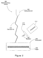
- Figures 2 and 3 are schematics of an apparatus 200 for detecting wear in a component 202 of an electrical device in accordance with an embodiment of the present invention.
- Figure 2 illustrates the apparatus 200 at an initial time
- Figure 3 illustrates the apparatus at a later time.
- a component 202 of an electrical device (not shown) has a tracer material 204 embedded in it at a predetermined depth.
- the component 202 is exposed to an electrical arc 206 that is generated by an electrical arcing element 208.
- the high temperature of the electrical arc 206 causes the portion of the component 202 that is exposed to the electrical arc 206 to emit electromagnetic radiation 207 that is continuously monitored by an electromagnetic detector, which may be a photodiode 210 or any other suitable detector for electromagnetic radiation (such as a spectrophotometer).
- an electromagnetic detector which may be a photodiode 210 or any other suitable detector for electromagnetic radiation (such as a spectrophotometer).
- a narrow band filter 212 is placed between the photodiode 210 and the component 202 of the electrical device so that the photodiode 210 is allowed to detect electromagnetic radiation having a wavelength in the narrow band that can pass through the narrow band filter 212.
- the electromagnetic radiation 207 has not been transmitted through the narrow band filter 212 because the electromagnetic radiation 207 was not emitted by the tracer material 204.
- the electromagnetic detector is capable of monitoring the component 202 of the electrical device continuously during the operation of the electrical device.
- Figure 3 is a schematic of the apparatus 200 in Figure 2, but at a later time after the component 202 has been worn.
- Figure 3 shows the tracer material 204 on a surface of the component 202, instead of embedded in the component at a predetermined depth.
- the surface of the component 202 has been worn away as a result of exposure to the electrical arc 206 or other causes, such as mechanical friction, so that the tracer material 204 is exposed to the electrical arc 206.
- the high temperature of the electrical arc 206 causes the tracer material 204 to emit electromagnetic radiation 209.
- the tracer material 204 is selected so that when it is exposed to the electrical arc 206, it emits electromagnetic radiation 209 that is distinct from the electromagnetic radiation 207 ( Figure 2) emitted by any other parts of the component that are exposed to the electrical arc.
- electromagnetic radiation 209 that is distinct from the electromagnetic radiation 207 ( Figure 2) emitted by any other parts of the component that are exposed to the electrical arc.
- lithium which emits red light corresponding to a wavelength of approximately 670.7 nm
- the materials that may be suitable for use as a tracer material in accordance with this invention are lithium, cobalt, niobium and rare earth metals such as yttrium.
- the electromagnetic radiation 209 has been transmitted through the narrow band filter 212 because the electromagnetic radiation 209 was emitted by the tracer material 204.
- the electromagnetic radiation emitted by the tracer material 204 when it is exposed to the electrical arc 206 is detected by a photodiode 210 after the electromagnetic radiation has passed through a narrow band filter 212.
- the narrow band filter removes electromagnetic radiation with a wavelength outside the narrow band that is transmitted by the narrow band filter 212.
- the narrow band filter 212 is selected so that it transmits electromagnetic radiation that is emitted by the tracer material when it is exposed to the electrical arc, but not electromagnetic radiation emitted by other parts of the component 202.
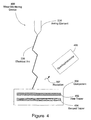
- Figure 4 is a schematic of an apparatus 400 for detecting two amounts of wear in a component 202 of an electrical device in accordance with an alternate embodiment of the present invention.
- a first tracer material 402 is embedded at one depth within the component 202 and a second tracer material 404 is embedded at another depth within the component 202.
- the first tracer material 402 and the second tracer material 404 are selected so that when they are exposed to the electrical arc 206, they emit electromagnetic radiation that is distinct from each other as well as from the radiation emitted by any other parts of the component that are exposed to the electrical arc.
- a spectrophotometer 406 analyzes electromagnetic radiation from the component 202 to determine whether the surface of the component 202 has worn to expose either the first tracer material 402 or the second tracer material 404.
- two photodiodes with differing narrow band filters may be used to monitor electromagnetic radiation from the first tracer material 402 and the second tracer material 404.
- Additional tracer materials (not shown) may be imbedded in the component 202 at various depths and/or at different locations in order to estimate the extent and/or location of wear of the component 202 according to which of the tracer materials is exposed to the electrical arc 206.
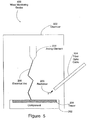
- FIG. 5 is a schematic of an apparatus 500 for detecting wear in a component 202 of an electrical device in accordance with an alternate embodiment of the present invention.
- an arcing element 208 and a component 202 having an embedded tracer material 204 are placed in an equipment chamber 502 and a fiber optic cable 504 is used to transmit electromagnetic radiation emitted by the component to an electromagnetic detector (not shown) outside the equipment chamber 502.
- FIG. 6 is a cross-sectional view of a diverter switch assembly 600 of a load tap changer in accordance with an embodiment of the invention.
- the diverter switch assembly 600 includes an arcing contact tip assembly 602 at one end of the diverter switch assembly and a compression spring 604 at its opposite end.
- the arcing contact tip assembly 602 may include an elkonite contact 606.
- tracer material 608 is embedded within the elkonite contact 606.
- the tracer material 608 will become exposed to an electrical arc (not shown) after the surface of the elkonite contact 606 is worn away, and an electromagnetic detector (not shown) will detect the distinctive electromagnetic radiation emitted by the tracer material 608.
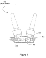
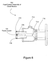
- Figures 7, 8 and 9 are, respectively, partially cut away cross-sectional views of a circuit breaker 700, the fixed contact assembly 702 of the circuit breaker 700, and the moving contact assembly 708 of the circuit breaker 700 in accordance with an embodiment of the invention.
- Figure 7 shows a circuit breaker 700, comprised of a fixed contact assembly 702 with a fixed contact pin 706, a tank 704, and a moving contact assembly 708.
- Figure 8 shows a fixed contact assembly 702 of a circuit breaker 700, comprised of shielding 710, a multicontact liner and a clamping ring 712, a contact pin holder 714, insulating support 716, a contact crown 718, and a fixed contact pin 706.
- tracer material 720 is embedded within the fixed contact pin 706.
- the tracer material 720 will become exposed to an electrical arc (not shown) after the surface of the fixed contact pin 706 is worn away, and an electromagnetic detector (not shown) will detect the distinctive electromagnetic radiation emitted by the tracer material 720.
- Figure 9 shows a moving contact assembly 708 of a circuit breaker 700, comprised of a main contact 722.
- tracer materials 724 and 726 are embedded within the main contact 722.
- the tracer materials 724 and 726 will become exposed to an electrical arc (not shown) after the surface of the main contact 722 is worn away, and an electromagnetic detector (not shown) will detect the distinctive electromagnetic radiation emitted by the tracer materials 724 and 726.
Landscapes
- General Physics & Mathematics (AREA)
- Health & Medical Sciences (AREA)
- Physics & Mathematics (AREA)
- Analytical Chemistry (AREA)
- General Health & Medical Sciences (AREA)
- Nuclear Medicine, Radiotherapy & Molecular Imaging (AREA)
- Life Sciences & Earth Sciences (AREA)
- Chemical & Material Sciences (AREA)
- Engineering & Computer Science (AREA)
- Biochemistry (AREA)
- Theoretical Computer Science (AREA)
- Immunology (AREA)
- Pathology (AREA)
- Arc-Extinguishing Devices That Are Switches (AREA)
- Measurement Of Length, Angles, Or The Like Using Electric Or Magnetic Means (AREA)
- Treatment Of Fiber Materials (AREA)
- Investigating, Analyzing Materials By Fluorescence Or Luminescence (AREA)
- Gas-Insulated Switchgears (AREA)
Claims (17)
- Verfahren zur Erkennung der Abnutzung in einer Komponente (202) einer elektrischen Vorrichtung, umfassend: Betreiben einer Komponente (202) einer elektrischen Vorrichtung, dadurch Erodieren (104) der Komponente (202) und Freilegen eines Tracer-Materials (204), das in einer vorbestimmten Tiefe der Komponente (202) eingebettet ist, bezüglich eines elektrischen Lichtbogens (206), was Emittieren elektromagnetischer Strahlung seitens des Tracer-Materials (204) und Erkennen (106) der vom Tracer-Material (204) emittierten elektromagnetischen Strahlung bewirkt.
- Verfahren nach Anspruch 1, wobei die elektromagnetische Strahlung unterschiedlich von elektromagnetischer Strahlung ist, die von irgendwelchen anderen Teilen der Komponente (202) emittiert wird, wenn die Komponente (202) dem elektrischen Lichtbogen (206) ausgesetzt wird.
- Verfahren nach Anspruch 1 oder Anspruch 2, das kontinuierliche Überwachung der Komponente (202) umfasst, um die vom Tracer-Material (204) emittierte elektromagnetische Strahlung zu erkennen.
- Verfahren nach einem beliebigen der vorhergehenden Ansprüche, das Einbettung des Tracer-Materials (204) in die Komponente (202) in einer vorbestimmten Tiefe umfasst.
- Verfahren nach einem beliebigen der vorhergehenden Ansprüche, wobei Erkennen der vom Tracer-Material (204) emittierten elektromagnetischen Strahlung die Verwendung einer Fotodiode (210) mit einem Schmalbandfilter für elektromagnetische Strahlung involviert.
- Verfahren nach einem beliebigen der Ansprüche 1 bis 4, wobei Erkennen der vom Tracer-Material (204) emittierten elektromagnetischen Strahlung die Verwendung eines Spektrofotometers (406) involviert.
- Verfahren nach einem beliebigen der vorhergehenden Ansprüche, wobei das Tracer-Material (204) aus einer Gruppe selektiert wird, die aus Lithium, Kobalt, Niob und Seltenerdmetall besteht.
- Verfahren nach einem beliebigen der vorhergehenden Ansprüche, wobei das Tracer-Material (204) ein erstes Tracer-Material (402), das fähig ist, eine erste elektromagnetische Strahlung zu emittieren und ein zweites Tracer-Material (404), das fähig ist, eine zweite elektromagnetische Strahlung zu emittieren, umfasst, die von der ersten elektromagnetischen Strahlung verschieden ist, wobei das erste Tracer-Material (402) in einer ersten vorbestimmten Tiefe in der Komponente (202) bereitgestellt ist und das zweite Tracer-Material (404) in einer zweiten vorbestimmten Tiefe (202) bereitgestellt ist, wobei das Verfahren umfasst: Betreiben und dadurch Erodieren der Komponente (202) und Freilegen des ersten Tracer-Materials (402) bezüglich eines elektrischen Lichtbogens (206), wodurch das Emittieren der ersten elektromagnetischen Strahlung vom ersten Tracer-Material (402) bewirkt wird; fortdauerndes Betreiben und dadurch Erodieren der Komponente (202) und Freilegen des zweiten Tracer-Materials (404) bezüglich eines elektrischen Lichtbogens (206), wodurch das Emittieren der zweiten elektromagnetischen Strahlung bewirkt wird; und Erkennen der ersten und zweiten emittierten elektromagnetischen Strahlung.
- Verfahren nach Anspruch 8, wobei das Erkennen der ersten elektromagnetischen Strahlung und das Erkennen der zweiten elektromagnetischen Strahlung kontinuierlich die Überwachung der Komponente (202) umfasst, um die erste vom ersten Tracer-Material (402) emittierte erste elektromagnetische Strahlung und die vom zweiten Tracer-Material (404) emittierte zweite elektromagnetische Strahlung zu überwachen.
- System zur Erkennung von Abnutzung in einem elektrischen Gerät, wobei die Vorrichtung umfasst: Eine Komponente (202) eines Geräts, das einem elektrischen Lichtbogen (206) ausgesetzt ist; ein Tracer-Material (204), das in einer vorbestimmten Tiefe in der Komponente (202) eingebettet ist, wobei das Tracer-Material (204) fähig ist, elektromagnetische Strahlung zu emittieren, wenn es dem elektrischen Lichtbogen (206) ausgesetzt wird und die vom Tracer-Material (204) emittierte elektromagnetische Strahlung ist verschieden von elektromagnetischer Strahlung, die von irgendwelchen anderen Teilen der Komponente (202) emittiert wird, wenn die Komponente (202) dem elektrischen Lichtbogen (206) ausgesetzt wird und einen elektromagnetischen Detektor, der konfiguriert ist, die Komponente (202) auf die vom Tracer-Material (204) emittierte elektromagnetische Strahlung zu überwachen.
- System nach Anspruch 10, wobei das Tracer-Material (204) ein erstes Tracer-Material (402), das in einer ersten vorbestimmten Tiefe in der Komponente (202) eingebettet ist, wobei das erste Tracer-Material (402) eine erste elektromagnetische Strahlung emittiert, wenn es dem elektrischen Lichtbogen (206) ausgesetzt wird und ein zweites Tracer-Material (404) umfasst, das in einer zweiten vorbestimmten Tiefe in der Komponente (202) eingebettet ist, wobei das zweite Tracer-Material (404) eine zweite elektromagnetische Strahlung emittiert, wenn es dem elektrischen Lichtbogen (206) ausgesetzt wird und der elektromagnetische Detektor konfiguriert ist, die Komponente (202) auf erste und zweite elektromagnetische Strahlung zu überwachen.
- System nach Anspruch 11, wobei der elektromagnetische Detektor einen ersten elektromagnetischen Detektor umfasst, der konfiguriert ist, die Komponente (202) auf die vom Tracer-Material (402) emittierte erste elektromagnetische Strahlung zu überwachen; und einen zweiten elektromagnetischen Detektor umfasst, der konfiguriert ist, die Komponente (202) auf die vom zweiten Tracer-Material (404) emittierte zweite elektromagnetische Strahlung zu überwachen.
- System nach einem beliebigen der Ansprüche 10 bis 12, wobei der elektromagnetische Detektor konfiguriert ist, die Komponente (202) kontinuierlich zu überwachen.
- System nach einem beliebigen der Ansprüche 10 bis 13, wobei der elektromagnetische Detektor eine Fotodiode (210) mit einem Schmalbandfilter für elektromagnetische Strahlung ist.
- System nach einem beliebigen der Ansprüche 10 bis 14, wobei der elektromagnetische Detektor ein Spektrofotometer (406) ist.
- System nach einem beliebigen der Ansprüche 10 bis 15, das weiter ein faseroptisches Kabel (504) umfasst, das konfiguriert ist, die elektromagnetische Strahlung an den elektromagnetischen Detektor zu übertragen.
- System nach einem beliebigen der Ansprüche 10 bis 16, wobei das Tracer-Material (204) aus der Gruppe selektiert wird, die aus Lithium, Kobalt, Niob und Seltenerdmetall besteht.
Applications Claiming Priority (3)
| Application Number | Priority Date | Filing Date | Title |
|---|---|---|---|
| US241108 | 2002-09-11 | ||
| US10/241,108 US6777948B2 (en) | 2002-09-11 | 2002-09-11 | Method and apparatus for detecting wear in components of high voltage electrical equipment |
| PCT/US2003/027532 WO2004025312A1 (en) | 2002-09-11 | 2003-09-04 | Method and apparatus for detecting wear in components of high voltage electrical equipment |
Publications (3)
| Publication Number | Publication Date |
|---|---|
| EP1537425A1 EP1537425A1 (de) | 2005-06-08 |
| EP1537425A4 EP1537425A4 (de) | 2006-05-17 |
| EP1537425B1 true EP1537425B1 (de) | 2007-06-06 |
Family
ID=31991106
Family Applications (1)
| Application Number | Title | Priority Date | Filing Date |
|---|---|---|---|
| EP03751964A Expired - Lifetime EP1537425B1 (de) | 2002-09-11 | 2003-09-04 | Verfahren und vorrichtung zur erkennung der abnutzung in komponenten von elektrischen hochspannungsgeräten |
Country Status (10)
| Country | Link |
|---|---|
| US (1) | US6777948B2 (de) |
| EP (1) | EP1537425B1 (de) |
| JP (1) | JP2006515419A (de) |
| AT (1) | ATE364183T1 (de) |
| AU (1) | AU2003270071B2 (de) |
| BR (1) | BR0314202A (de) |
| CA (1) | CA2498775C (de) |
| DE (1) | DE60314259T2 (de) |
| ES (1) | ES2288617T3 (de) |
| WO (1) | WO2004025312A1 (de) |
Families Citing this family (13)
| Publication number | Priority date | Publication date | Assignee | Title |
|---|---|---|---|---|
| US7053625B2 (en) * | 2002-09-11 | 2006-05-30 | Electric Power Research Institute, Inc. | Method and apparatus for detecting wear in components of high voltage electrical equipment |
| US7501646B2 (en) * | 2003-06-26 | 2009-03-10 | Ncr Corporation | Security markers for reducing receipt fraud |
| US7488954B2 (en) * | 2003-06-26 | 2009-02-10 | Ncr Corporation | Security markers for marking a person or property |
| US7378675B2 (en) * | 2003-06-26 | 2008-05-27 | Ncr Corporation | Security markers for indicating condition of an item |
| JP4334299B2 (ja) * | 2003-08-22 | 2009-09-30 | 株式会社東芝 | 電気接点、電気接点摩耗検出装置およびその摩耗検出方法 |
| US7023217B1 (en) | 2004-12-16 | 2006-04-04 | Honeywell International Inc. | Method and apparatus for determining wear of resistive and conductive elements |
| CN101438363A (zh) * | 2006-04-07 | 2009-05-20 | 瓦格厦电气系统公司 | 监测通电抽头变换器隔间内的位移的系统和方法 |
| EP1895554A1 (de) * | 2006-09-04 | 2008-03-05 | ABB Research Ltd | Elektrischer Kontakt mit Signal-Zone zum Signalisieren von Kontaktverschleiss |
| JP5032091B2 (ja) * | 2006-10-12 | 2012-09-26 | 株式会社東芝 | ガス絶縁開閉装置及びガス絶縁開閉装置用部品のアーク損傷検出方法 |
| USD569285S1 (en) * | 2007-05-08 | 2008-05-20 | Zts, Inc. | Battery tester |
| USD611851S1 (en) * | 2009-07-09 | 2010-03-16 | Zts, Inc. | Battery tester |
| US9885659B1 (en) | 2016-10-04 | 2018-02-06 | International Business Machines Corporation | Method to determine connector metal wear via flouresence |
| US11181462B2 (en) | 2018-11-30 | 2021-11-23 | International Business Machines Corporation | Non-destructive method to determine porosity in metallic coatings |
Family Cites Families (7)
| Publication number | Priority date | Publication date | Assignee | Title |
|---|---|---|---|---|
| US3715598A (en) * | 1969-06-12 | 1973-02-06 | G Tomlin | Integral fault detection system for operating electronics equipment |
| JPH0722151B2 (ja) * | 1984-05-23 | 1995-03-08 | 株式会社日立製作所 | エツチングモニタ−方法 |
| US5389792A (en) * | 1993-01-04 | 1995-02-14 | Grumman Aerospace Corporation | Electron microprobe utilizing thermal detector arrays |
| US5453591A (en) | 1994-04-05 | 1995-09-26 | Abb Power T&D Company Inc. | Sensing structure for component wear in high voltage circuit interrupters |
| WO1996013732A1 (de) | 1994-10-27 | 1996-05-09 | Siemens Aktiengesellschaft | Verfahren zum überwachen des abbrandes wenigstens eines kontaktstückes bei einem schaltgerät sowie diesbezüglich ausgebildetes schaltgerät |
| JPH0961357A (ja) * | 1995-08-25 | 1997-03-07 | Kawasaki Steel Corp | 発光分光分析による微少非金属介在物の定量方法 |
| US5941370A (en) | 1996-09-10 | 1999-08-24 | Nichols; Bruce W. | Electrical contact wear |
-
2002
- 2002-09-11 US US10/241,108 patent/US6777948B2/en not_active Expired - Fee Related
-
2003
- 2003-09-04 BR BR0314202-7A patent/BR0314202A/pt not_active IP Right Cessation
- 2003-09-04 EP EP03751964A patent/EP1537425B1/de not_active Expired - Lifetime
- 2003-09-04 DE DE60314259T patent/DE60314259T2/de not_active Expired - Lifetime
- 2003-09-04 ES ES03751964T patent/ES2288617T3/es not_active Expired - Lifetime
- 2003-09-04 AT AT03751964T patent/ATE364183T1/de not_active IP Right Cessation
- 2003-09-04 WO PCT/US2003/027532 patent/WO2004025312A1/en not_active Ceased
- 2003-09-04 AU AU2003270071A patent/AU2003270071B2/en not_active Ceased
- 2003-09-04 CA CA002498775A patent/CA2498775C/en not_active Expired - Fee Related
- 2003-09-04 JP JP2004536084A patent/JP2006515419A/ja active Pending
Non-Patent Citations (1)
| Title |
|---|
| None * |
Also Published As
| Publication number | Publication date |
|---|---|
| EP1537425A4 (de) | 2006-05-17 |
| WO2004025312A1 (en) | 2004-03-25 |
| BR0314202A (pt) | 2005-07-12 |
| US20040046563A1 (en) | 2004-03-11 |
| DE60314259D1 (de) | 2007-07-19 |
| JP2006515419A (ja) | 2006-05-25 |
| DE60314259T2 (de) | 2008-01-31 |
| US6777948B2 (en) | 2004-08-17 |
| ATE364183T1 (de) | 2007-06-15 |
| CA2498775C (en) | 2009-08-18 |
| ES2288617T3 (es) | 2008-01-16 |
| AU2003270071A1 (en) | 2004-04-30 |
| CA2498775A1 (en) | 2004-03-25 |
| EP1537425A1 (de) | 2005-06-08 |
| AU2003270071B2 (en) | 2007-10-18 |
Similar Documents
| Publication | Publication Date | Title |
|---|---|---|
| EP1537425B1 (de) | Verfahren und vorrichtung zur erkennung der abnutzung in komponenten von elektrischen hochspannungsgeräten | |
| EP1335466B1 (de) | Selbstversorgende Vorrichtung und Verfahren zum optischen Erfassen von Lichtbogenfehlern in elektrischen Leistungssystemen in Gegenwart von anderen LIchtquellen | |
| US4532499A (en) | Means for detecting the contact wear of electrical switching devices | |
| JP4334299B2 (ja) | 電気接点、電気接点摩耗検出装置およびその摩耗検出方法 | |
| US7038201B2 (en) | Method and apparatus for determining electrical contact wear | |
| CN1082709C (zh) | 电触点磨损和温度指示剂 | |
| CN113439318A (zh) | 真空断路器用触头监测装置及包括该装置的真空断路器 | |
| EP1626268B1 (de) | Verfahren und Vorrichtung zur Erkennung der Abnutzung in Komponenten von elektrischen Hochspannungsgeräten | |
| JP2007538371A (ja) | 真空開閉装置における高圧条件を検出する方法および装置 | |
| US20040113070A1 (en) | Method and apparatus for determining electrical contact wear | |
| EP4369372A1 (de) | Vakuumschalter, transformatoranordnung und verfahren zur überwachung eines vakuumschalters | |
| KR20190053887A (ko) | 안전 장치의 작동 방법 | |
| CA1292029C (en) | Operation-indicator device for fuse cartridges for electrical protection | |
| EP3163685B1 (de) | Schutzabdeckung und elektrischer verbinder mit strahlungsfenster, das durch eine vielzahl von strahlungsdurchgängen ausgebildet ist | |
| HK1095201B (en) | Device for detecting contact wear in switching appliances | |
| HK1095201A1 (zh) | 采集开关设备中触点烧损的装置 | |
| CA1257633A (en) | Load break switch with insulating gas in sealed housing | |
| JPS60198011A (ja) | 接点寿命監視装置 | |
| HK1022778B (en) | Electrical contact wear and temperature indicator | |
| NO851407L (no) | Lastbryter med sikkerhetsmekanisme. |
Legal Events
| Date | Code | Title | Description |
|---|---|---|---|
| PUAI | Public reference made under article 153(3) epc to a published international application that has entered the european phase |
Free format text: ORIGINAL CODE: 0009012 |
|
| 17P | Request for examination filed |
Effective date: 20050321 |
|
| AK | Designated contracting states |
Kind code of ref document: A1 Designated state(s): AT BE BG CH CY CZ DE DK EE ES FI FR GB GR HU IE IT LI LU MC NL PT RO SE SI SK TR |
|
| AX | Request for extension of the european patent |
Extension state: AL LT LV MK |
|
| DAX | Request for extension of the european patent (deleted) | ||
| A4 | Supplementary search report drawn up and despatched |
Effective date: 20060403 |
|
| RIC1 | Information provided on ipc code assigned before grant |
Ipc: G01R 31/02 20060101AFI20040327BHEP Ipc: G01R 31/327 20060101ALI20060328BHEP Ipc: G01N 21/67 20060101ALI20060328BHEP |
|
| GRAP | Despatch of communication of intention to grant a patent |
Free format text: ORIGINAL CODE: EPIDOSNIGR1 |
|
| GRAS | Grant fee paid |
Free format text: ORIGINAL CODE: EPIDOSNIGR3 |
|
| GRAA | (expected) grant |
Free format text: ORIGINAL CODE: 0009210 |
|
| AK | Designated contracting states |
Kind code of ref document: B1 Designated state(s): AT BE BG CH CY CZ DE DK EE ES FI FR GB GR HU IE IT LI LU MC NL PT RO SE SI SK TR |
|
| PG25 | Lapsed in a contracting state [announced via postgrant information from national office to epo] |
Ref country code: FI Free format text: LAPSE BECAUSE OF FAILURE TO SUBMIT A TRANSLATION OF THE DESCRIPTION OR TO PAY THE FEE WITHIN THE PRESCRIBED TIME-LIMIT Effective date: 20070606 |
|
| REG | Reference to a national code |
Ref country code: GB Ref legal event code: FG4D |
|
| REG | Reference to a national code |
Ref country code: CH Ref legal event code: EP |
|
| REG | Reference to a national code |
Ref country code: IE Ref legal event code: FG4D |
|
| REF | Corresponds to: |
Ref document number: 60314259 Country of ref document: DE Date of ref document: 20070719 Kind code of ref document: P |
|
| REG | Reference to a national code |
Ref country code: SE Ref legal event code: TRGR |
|
| REG | Reference to a national code |
Ref country code: CH Ref legal event code: NV Representative=s name: RITSCHER & PARTNER AG |
|
| ET | Fr: translation filed | ||
| NLV1 | Nl: lapsed or annulled due to failure to fulfill the requirements of art. 29p and 29m of the patents act | ||
| PG25 | Lapsed in a contracting state [announced via postgrant information from national office to epo] |
Ref country code: BE Free format text: LAPSE BECAUSE OF FAILURE TO SUBMIT A TRANSLATION OF THE DESCRIPTION OR TO PAY THE FEE WITHIN THE PRESCRIBED TIME-LIMIT Effective date: 20070606 |
|
| REG | Reference to a national code |
Ref country code: ES Ref legal event code: FG2A Ref document number: 2288617 Country of ref document: ES Kind code of ref document: T3 |
|
| PG25 | Lapsed in a contracting state [announced via postgrant information from national office to epo] |
Ref country code: SI Free format text: LAPSE BECAUSE OF FAILURE TO SUBMIT A TRANSLATION OF THE DESCRIPTION OR TO PAY THE FEE WITHIN THE PRESCRIBED TIME-LIMIT Effective date: 20070606 Ref country code: PT Free format text: LAPSE BECAUSE OF FAILURE TO SUBMIT A TRANSLATION OF THE DESCRIPTION OR TO PAY THE FEE WITHIN THE PRESCRIBED TIME-LIMIT Effective date: 20071106 Ref country code: NL Free format text: LAPSE BECAUSE OF FAILURE TO SUBMIT A TRANSLATION OF THE DESCRIPTION OR TO PAY THE FEE WITHIN THE PRESCRIBED TIME-LIMIT Effective date: 20070606 Ref country code: CZ Free format text: LAPSE BECAUSE OF FAILURE TO SUBMIT A TRANSLATION OF THE DESCRIPTION OR TO PAY THE FEE WITHIN THE PRESCRIBED TIME-LIMIT Effective date: 20070606 Ref country code: BG Free format text: LAPSE BECAUSE OF FAILURE TO SUBMIT A TRANSLATION OF THE DESCRIPTION OR TO PAY THE FEE WITHIN THE PRESCRIBED TIME-LIMIT Effective date: 20070906 |
|
| PG25 | Lapsed in a contracting state [announced via postgrant information from national office to epo] |
Ref country code: SK Free format text: LAPSE BECAUSE OF FAILURE TO SUBMIT A TRANSLATION OF THE DESCRIPTION OR TO PAY THE FEE WITHIN THE PRESCRIBED TIME-LIMIT Effective date: 20070606 |
|
| PLBE | No opposition filed within time limit |
Free format text: ORIGINAL CODE: 0009261 |
|
| STAA | Information on the status of an ep patent application or granted ep patent |
Free format text: STATUS: NO OPPOSITION FILED WITHIN TIME LIMIT |
|
| REG | Reference to a national code |
Ref country code: CH Ref legal event code: PCAR Free format text: RITSCHER & PARTNER AG;RESIRAIN 1;8125 ZOLLIKERBERG (CH) |
|
| PG25 | Lapsed in a contracting state [announced via postgrant information from national office to epo] |
Ref country code: GR Free format text: LAPSE BECAUSE OF FAILURE TO SUBMIT A TRANSLATION OF THE DESCRIPTION OR TO PAY THE FEE WITHIN THE PRESCRIBED TIME-LIMIT Effective date: 20070907 Ref country code: MC Free format text: LAPSE BECAUSE OF NON-PAYMENT OF DUE FEES Effective date: 20070930 Ref country code: DK Free format text: LAPSE BECAUSE OF FAILURE TO SUBMIT A TRANSLATION OF THE DESCRIPTION OR TO PAY THE FEE WITHIN THE PRESCRIBED TIME-LIMIT Effective date: 20070606 |
|
| 26N | No opposition filed |
Effective date: 20080307 |
|
| PG25 | Lapsed in a contracting state [announced via postgrant information from national office to epo] |
Ref country code: RO Free format text: LAPSE BECAUSE OF FAILURE TO SUBMIT A TRANSLATION OF THE DESCRIPTION OR TO PAY THE FEE WITHIN THE PRESCRIBED TIME-LIMIT Effective date: 20070606 |
|
| PG25 | Lapsed in a contracting state [announced via postgrant information from national office to epo] |
Ref country code: IE Free format text: LAPSE BECAUSE OF NON-PAYMENT OF DUE FEES Effective date: 20070904 |
|
| PGFP | Annual fee paid to national office [announced via postgrant information from national office to epo] |
Ref country code: AT Payment date: 20080811 Year of fee payment: 6 |
|
| PG25 | Lapsed in a contracting state [announced via postgrant information from national office to epo] |
Ref country code: EE Free format text: LAPSE BECAUSE OF FAILURE TO SUBMIT A TRANSLATION OF THE DESCRIPTION OR TO PAY THE FEE WITHIN THE PRESCRIBED TIME-LIMIT Effective date: 20070606 |
|
| PG25 | Lapsed in a contracting state [announced via postgrant information from national office to epo] |
Ref country code: CY Free format text: LAPSE BECAUSE OF FAILURE TO SUBMIT A TRANSLATION OF THE DESCRIPTION OR TO PAY THE FEE WITHIN THE PRESCRIBED TIME-LIMIT Effective date: 20070606 |
|
| PG25 | Lapsed in a contracting state [announced via postgrant information from national office to epo] |
Ref country code: LU Free format text: LAPSE BECAUSE OF NON-PAYMENT OF DUE FEES Effective date: 20070904 |
|
| PG25 | Lapsed in a contracting state [announced via postgrant information from national office to epo] |
Ref country code: HU Free format text: LAPSE BECAUSE OF FAILURE TO SUBMIT A TRANSLATION OF THE DESCRIPTION OR TO PAY THE FEE WITHIN THE PRESCRIBED TIME-LIMIT Effective date: 20071207 |
|
| PG25 | Lapsed in a contracting state [announced via postgrant information from national office to epo] |
Ref country code: AT Free format text: LAPSE BECAUSE OF NON-PAYMENT OF DUE FEES Effective date: 20090904 |
|
| PGFP | Annual fee paid to national office [announced via postgrant information from national office to epo] |
Ref country code: DE Payment date: 20120928 Year of fee payment: 10 |
|
| PGFP | Annual fee paid to national office [announced via postgrant information from national office to epo] |
Ref country code: SE Payment date: 20130624 Year of fee payment: 11 |
|
| PGFP | Annual fee paid to national office [announced via postgrant information from national office to epo] |
Ref country code: CH Payment date: 20130806 Year of fee payment: 11 Ref country code: ES Payment date: 20130822 Year of fee payment: 11 |
|
| PGFP | Annual fee paid to national office [announced via postgrant information from national office to epo] |
Ref country code: TR Payment date: 20130703 Year of fee payment: 11 Ref country code: GB Payment date: 20130726 Year of fee payment: 11 Ref country code: FR Payment date: 20130712 Year of fee payment: 11 |
|
| REG | Reference to a national code |
Ref country code: CH Ref legal event code: PFA Owner name: ELECTRIC POWER RESEARCH INSTITUTE, INC, US Free format text: FORMER OWNER: ELECTRIC POWER RESEARCH INSTITUTE, INC, US |
|
| PGFP | Annual fee paid to national office [announced via postgrant information from national office to epo] |
Ref country code: IT Payment date: 20130627 Year of fee payment: 11 |
|
| REG | Reference to a national code |
Ref country code: DE Ref legal event code: R119 Ref document number: 60314259 Country of ref document: DE Effective date: 20140401 |
|
| PG25 | Lapsed in a contracting state [announced via postgrant information from national office to epo] |
Ref country code: DE Free format text: LAPSE BECAUSE OF NON-PAYMENT OF DUE FEES Effective date: 20140401 |
|
| REG | Reference to a national code |
Ref country code: CH Ref legal event code: PL |
|
| REG | Reference to a national code |
Ref country code: SE Ref legal event code: EUG |
|
| GBPC | Gb: european patent ceased through non-payment of renewal fee |
Effective date: 20140904 |
|
| PG25 | Lapsed in a contracting state [announced via postgrant information from national office to epo] |
Ref country code: SE Free format text: LAPSE BECAUSE OF NON-PAYMENT OF DUE FEES Effective date: 20140905 |
|
| REG | Reference to a national code |
Ref country code: FR Ref legal event code: ST Effective date: 20150529 |
|
| PG25 | Lapsed in a contracting state [announced via postgrant information from national office to epo] |
Ref country code: GB Free format text: LAPSE BECAUSE OF NON-PAYMENT OF DUE FEES Effective date: 20140904 Ref country code: LI Free format text: LAPSE BECAUSE OF NON-PAYMENT OF DUE FEES Effective date: 20140930 Ref country code: CH Free format text: LAPSE BECAUSE OF NON-PAYMENT OF DUE FEES Effective date: 20140930 |
|
| PG25 | Lapsed in a contracting state [announced via postgrant information from national office to epo] |
Ref country code: IT Free format text: LAPSE BECAUSE OF NON-PAYMENT OF DUE FEES Effective date: 20140904 Ref country code: FR Free format text: LAPSE BECAUSE OF NON-PAYMENT OF DUE FEES Effective date: 20140930 |
|
| REG | Reference to a national code |
Ref country code: ES Ref legal event code: FD2A Effective date: 20151026 |
|
| PG25 | Lapsed in a contracting state [announced via postgrant information from national office to epo] |
Ref country code: ES Free format text: LAPSE BECAUSE OF NON-PAYMENT OF DUE FEES Effective date: 20140905 |
|
| PG25 | Lapsed in a contracting state [announced via postgrant information from national office to epo] |
Ref country code: TR Free format text: LAPSE BECAUSE OF NON-PAYMENT OF DUE FEES Effective date: 20140904 |