EP1536515A1 - Antenna device - Google Patents
Antenna device Download PDFInfo
- Publication number
- EP1536515A1 EP1536515A1 EP04027521A EP04027521A EP1536515A1 EP 1536515 A1 EP1536515 A1 EP 1536515A1 EP 04027521 A EP04027521 A EP 04027521A EP 04027521 A EP04027521 A EP 04027521A EP 1536515 A1 EP1536515 A1 EP 1536515A1
- Authority
- EP
- European Patent Office
- Prior art keywords
- conductor plate
- antenna device
- radiating conductor
- stopper portion
- portions
- Prior art date
- Legal status (The legal status is an assumption and is not a legal conclusion. Google has not performed a legal analysis and makes no representation as to the accuracy of the status listed.)
- Withdrawn
Links
- 239000004020 conductor Substances 0.000 claims abstract description 134
- 238000003780 insertion Methods 0.000 claims abstract description 11
- 230000037431 insertion Effects 0.000 claims abstract description 11
- 239000002184 metal Substances 0.000 claims abstract description 10
- 238000010586 diagram Methods 0.000 description 8
- 238000000034 method Methods 0.000 description 8
- 239000000758 substrate Substances 0.000 description 5
- 230000005684 electric field Effects 0.000 description 4
- 238000005452 bending Methods 0.000 description 2
- 230000003247 decreasing effect Effects 0.000 description 2
- 230000002349 favourable effect Effects 0.000 description 2
- 230000000149 penetrating effect Effects 0.000 description 2
- 238000007789 sealing Methods 0.000 description 2
- 239000000853 adhesive Substances 0.000 description 1
- 230000001070 adhesive effect Effects 0.000 description 1
- 230000007423 decrease Effects 0.000 description 1
- 239000011810 insulating material Substances 0.000 description 1
- 238000004519 manufacturing process Methods 0.000 description 1
- 230000000717 retained effect Effects 0.000 description 1
- 238000005476 soldering Methods 0.000 description 1
Images






Classifications
-
- H—ELECTRICITY
- H01—ELECTRIC ELEMENTS
- H01Q—ANTENNAS, i.e. RADIO AERIALS
- H01Q1/00—Details of, or arrangements associated with, antennas
- H01Q1/27—Adaptation for use in or on movable bodies
- H01Q1/32—Adaptation for use in or on road or rail vehicles
- H01Q1/3208—Adaptation for use in or on road or rail vehicles characterised by the application wherein the antenna is used
- H01Q1/3233—Adaptation for use in or on road or rail vehicles characterised by the application wherein the antenna is used particular used as part of a sensor or in a security system, e.g. for automotive radar, navigation systems
-
- H—ELECTRICITY
- H01—ELECTRIC ELEMENTS
- H01Q—ANTENNAS, i.e. RADIO AERIALS
- H01Q9/00—Electrically-short antennas having dimensions not more than twice the operating wavelength and consisting of conductive active radiating elements
- H01Q9/04—Resonant antennas
- H01Q9/0407—Substantially flat resonant element parallel to ground plane, e.g. patch antenna
Definitions
- the present invention relates to a patch antenna device which can be suitably used for a GPS antenna or the like.
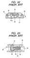
- Fig. 22 is a cross-sectional view showing schematically an overall configuration of a conventional antenna device
- Fig. 23 is an expanded cross-sectional view showing essential parts of the conventional antenna device.
- a configuration of the conventional antenna device will be described with reference to Figs. 22 and 23.
- a ground conductor plate 52 is mounted on a top surface of a boxlike case 51.
- an antenna element 53 is mounted to an upper end portion of a post 51a which is provided to project into the case 51.
- a shield cover 54 is mounted, and a coaxial cable 55 is inserted in a cavity of the shield cover 54.
- An outer conductor 56 of the coaxial cable 55 is soldered to the shield cover 54, and simultaneously a central conductor 57 of the coaxial cable 55 is bent upward and then supported by a holding member 58.
- the central conductor 57 supported by the holding member 58 is connected to the antenna element 53.
- a cuplike cover 59 is mounted on the case 51 to cover the antenna element 53, so that the conventional antenna device is constructed (for example, see Japanese Unexamined Patent Application Publication No. 2003-60414).
- an object of the present invention to provide an inexpensive antenna device has decreased number of components and favorable assembling quality.
- an antenna device comprising an antenna main body portion having a circuit board on which a ground conductor plate made of a metal plate, a radiating conductor plate made of a metal plate and an electronic component are installed to form a desired electrical circuit, and a cable connected to the electrical circuit, in which the ground conductor plate has a stopper portion which is formed by cutting the ground conductor plate and raising the cut portion toward the radiating conductor plate, the stopper portion having an insertion portion provided therebelow, and the cable is inserted into the insertion portion and supported by the stopper portion.
- the cable is a coaxial cable having a central conductor and an outer conductor covering an outside of the central conductor, and the outer conductor is soldered to the stopper portion.
- a cut-out portion is provided in the stopper portion, and the outer conductor is soldered to the stopper portion at a position in the cut-out portion.
- At least a portion of a top surface of the stopper portion is arranged to face the radiating conductor plate in its vicinity of a circumferential edge portion of the radiating conductor plate.
- the stopper portion is arranged along a circumferential edge of the radiating conductor plate.
- the antenna device of the present invention comprises the antenna main body portion having the circuit board on which the ground conductor plate made of the metal plate, the radiating conductor plate made of the metal plate, and the electronic component are mounted to form the desired electrical circuit, and the cable connected to the electrical circuit.
- the ground conductor plate has the stopper portion which is formed by cutting the ground conductor plate and raising the cut portion toward the radiating conductor plate, the stopper portion having an insertion portion provided therebelow, and the cable is inserted into the insertion portion and supported by the stopper portion. According to this configuration, the cable can be supported by the stopper portion which is incorporated into the ground conductor plate. Therefore, an additional component for supporting the cable is not needed, and thus an inexpensive antenna device having decreased number of components and the favorable assembling quality can be obtained.
- the cable is the coaxial cable having the central conductor and the outer conductor covering the outside of the central conductor, and the outer conductor is soldered to the stopper portion.
- the cable can be securely supported.
- a cut-out portion is provided in the stopper portion, and the outer conductor is soldered to the stopper portion at a position in the cut-out portion.
- At least a portion of a top surface of the stopper portion is arranged to face the radiating conductor plate in the vicinity of a circumferential edge portion of the radiating conductor plate.
- the stopper portion is arranged along the outer circumferential edge of the radiating conductor plate.
- the stopper portion is arranged along the outer circumferential edge of the radiating conductor plate.
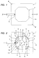
- Fig. 1 is a plan view showing an antenna device according to the present invention
- Fig. 2 is a plan view showing a state in which a cover is removed, in the antenna device according to the present invention
- Fig. 3 is a cross-sectional view taken along a line 3-3 of Fig. 1
- Fig. 4 is a cross-sectional view taken along a line 4-4 of Fig. 1.
- Fig. 5 is an exploded perspective view showing the antenna device according to the present invention.
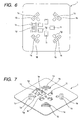
- Fig. 6 is a plan view showing a ground conductor plate of the antenna device according to the present invention
- Fig. 7 is a perspective view showing the ground conductor plate of the antenna device according to the present invention
- Fig. 8 is a plan view showing a circuit board of the antenna device according to the present invention
- Fig. 9 is a plan view showing a radiating conductor plate of the antenna device according to the present invention
- Fig. 10 is a front view showing the radiating conductor plate of the antenna device according to the present invention
- Fig. 11 is a bottom view showing the radiating conductor plate of the antenna device according to the present invention.
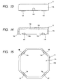
- Fig. 12 is a plan view showing a cover of the antenna device according to the present invention
- Fig. 13 is a left side view showing the cover of the antenna device according to the present invention
- Fig. 14 is a cross-sectional view showing schematically the cover of the antenna device according to the present invention
- Fig. 15 is a bottom view showing the cover of the antenna device according to the present invention.
- Fig. 16 is a diagram illustrating a first step of a mounting method of the radiating conductor plate on the circuit board, in the antenna device according to the present invention
- Fig. 17 is a diagram illustrating a second step of the mounting method of the radiating conductor plate on the circuit board, in the antenna device according to the present invention
- Fig. 18 is a diagram illustrating a third step of the mounting method of the radiating conductor plate on the circuit board, in the antenna device according to the present invention
- Fig. 19 is a perspective view showing a state in which the mounting of the radiating conductor plate on the circuit board is finished, in the antenna device according to the present invention.
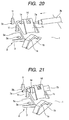
- Fig. 20 is a diagram illustrating a mounting method of a cable to the ground conductor plate, in the antenna device according to the present invention
- Fig. 21 is a perspective view showing a state in which the mounting of the cable to the ground conductor plate is finished, in the antenna device according to the present invention.
- a ground conductor plate 1 made of a metal plate, which serves as a ground conductor, has a plurality of hooking portions 1a, each being formed by cutting the ground conductor plate 1 and raising the cut portion upward in an arch shape in four directions, holes 1b arranged adjacent to the respective hooking portions 1a, a plurality of stopper portions 1c, each being positioned between adjacent two hooking portions 1a and being formed by cutting the ground conductor plate 1 and raising the cut portion upward in an arch shape, cut-out portions 1d, each being provided in a vicinity of a top portion of each stopper portion 1c and being made of a through hole, and insertion portions 1e provided below the respective stopper portions 1c, in particular, as shown in Figs. 6 and 7.
- ground conductor plate 1 has a plurality of bent pieces 1f bent upward, and escape portions 1g provided a plurality of positions which include positions adjacent to the respective bent pieces 1f.
- a rectangular circuit board 2 has a dielectric substrate 3 made of an insulating plate, a wiring pattern 4 provided in the dielectric substrate 3, and a plurality of electrodes 5a, 5b, 5c and 5d provided in four corners of the dielectric substrate 3, in particular, as shown in Fig. 8.
- the electrodes 5a, 5b, 5c and 5d are referred to as first, second, third, and fourth electrodes, respectively.
- first and second electrodes 5a and 5b or the third and fourth electrodes 5c and 5d, which face each other in an oblique direction, have the same area. Further, the first and second electrodes 5a and 5b have the areas smaller than those of the third and fourth electrodes 5c and 5d.
- the dielectric substrate 3 has a plurality of penetrating portions 3a respectively provided at positions of the first to fourth electrodes 5a to 5d as through holes, a plurality of first holes 3b provided in vicinities of an outer circumferential edge, and a plurality of second holes 3c provided in a central portion.
- circuit board 2 electronic components 6 including a short-height chip condenser and so on, or a tall dielectric filter 6a and so on are mounted, so that a desired electrical circuit having a matching circuit, a filter circuit, an amplifying circuit and so on is formed.
- the tall components 6 including the dielectric filter 6a are being arranged in the vicinities of the outer circumferential edge of the circuit board 2.
- Such a circuit board 2 is mounted on the ground conductor plate 1 such that a bottom surface of the circuit board 2 contacts the ground conductor plate 1 while the bent pieces 1f are inserted into the first holes 3b, in particular, as shown in Figs. 3 and 5.
- the bent pieces 1f are soldered to the wiring pattern 4, so that the circuit board 2 is supported by the bent pieces 1f.
- the first to fourth electrodes 5a to 5d face the ground conductor plate 1 with the dielectric substrate 3 interposed therebetween, and then condensers are respectively formed.
- a coaxial cable 7 has a central conductor 7a and a mesh-like outer conductor 7b provided by an insulating covered portion to cover an outside of the central conductor 7a.
- a front end portion of the cable 7 is inserted into the insertion portion 1e of the stopper portion 1c to be in a state as shown in Fig. 21.
- the central conductor 7a is soldered to the wiring pattern 4.
- the outer conductor 7b and the stopper portion 1c are soldered, so that the cable 7 is supported by the stopper portion 1c.
- An octagonal radiating conductor plate 8 made of a metal plate has two feeding portions of first and second feeding portions 9a and 9b, which are formed by cutting the radiating conductor plate 8 and bending the cut portion downward at positions which make a right angle, and adjusting means Z, provided on a line S1 passing through the first feeding portion 9a and a center C, and a line S2 passing through the second feeding portion 9b and the center C, for adjusting an electrical length, in particular, as shown in Figs. 9 to 11.
- the adjusting means Z are provided at the positions of the lines S1 and S2 which are the directions of the electric fields. At the same time, the adjusting means are provided at positions between the central portion and the outer circumferential edge, except for the central portion of the radiating conductor plate 8.
- the adjusting means Z are provided at opposite sides to the first and second feeding portions 9a and 9b therefrom beyond the center C. Further, the adjusting means Z are formed by ladder-like portions which holes 10a and crosspiece portions 10b combine and form. Here, by cutting the crosspiece portions 10b, the electrical lengths extend.
- the radiating conductor plate 8 has a pair of opposing sides 11a and 11b, each being positioned on lines S3 and S4 which pass through the center C and are orthogonal to each other, and four leg pieces 12a, 12b, 12c and 12d provided at positions any where on the lines S3 and S4 up to the first and second opposing sides 11a and 11b, except for the central portion.
- the four leg pieces 12a to 12d are respectively provided at positions spaced by the same distance from the center C to be bent downward. Further, the leg pieces 12a to 12d are provided at positions closer to the center than the first and second opposing sides 11a and 11b.
- the electric field intensity of the radiating conductor plate 8 is made strong in the outer circumferential portion on the lines S1 and S2.
- the leg pieces 12a to 12d are provided at positions, spaced apart from the lines S1 and S2, in which the electric field intensity is relatively weak.
- a locking portion 13 having a first locking piece 13a positioned at the lowest portion and a second locking piece 13b spaced by a predetermined gap from the first locking piece is provided.
- first and second locking pieces 13a and 13b are formed with bent portions which are bent in an opposite direction to each other with each leg piece 12a to 12d as a center.
- the radiating conductor plate 8 As regards the mounting of the radiating conductor plate 8 having such a configuration, first, as shown in Fig. 16, the radiating conductor plate 8 is arranged on the circuit board 2, and then, against the resilience of the leg pieces 12a to 12d, the leg pieces 12a to 12d are bent inward respectively.
- the leg pieces 12a to 12d return to the original states.
- the first locking piece 13a is locked to a rear surface of the circuit board 2 and the second locking piece 13b is locked to a front surface of the circuit board 2.
- the radiating conductor plate 8 is temporally retained to the circuit board 2.
- leg pieces 12a to 12d are respectively soldered and connected to the first to fourth electrodes 5a to 5d, and then the first and second feeding portions 9a and 9b are soldered to the wiring pattern 4 which is provided in vicinities of the second holes 3c.
- an antenna main body portion H is formed.
- leg pieces 12a to 12d and the first and second feeding portions 9a and 9b are not connected to the ground conductor plate 1 by means of the release holes 1g.
- the radiating conductor plate 8 mounted on the circuit board 2 in such a manner is arranged parallel to the ground conductor plate 1 and the circuit board 2 and is spaced by a predetermined gap therefrom. Further, the first electrical length of the radiating conductor plate 8 is determined by a length of the radiating conductor plate 8 on the line S1 and a capacitance of the condenser formed by the electrodes 5a and 5b. In addition, the second electrical length of the radiating conductor plate 8 is determined by a length of the radiating conductor plate 8 on the line S2 and a capacitance of the condenser formed by the electrodes 5c and 5d.
- the length of the radiating conductor plate 8 on the line S1 and the length of the radiating conductor plate 8 on the line S2 are the same, but the capacitance formed by the electrodes 5a and 5b is set to be smaller than the capacitance formed by the electrodes 5c and 5d.
- the first electrical length is smaller than the second electrical length, and then the difference between both electrical lengths is caused. As a result, a circularly polarized wave antenna device is obtained.
- the circuit board 2 is positioned within a planar region of the radiating conductor plate 8.
- the radiating conductor plate 8 when the radiating conductor plate 8 is mounted, upper surfaces of the hooking portions 1a, the stopper portions 1c and the tall electronic component 6a are arranged to face the vicinities of the circumferential edge portion of the radiating conductor plate 8. Further, the front end portions of the bent portions 1f are arranged to face the radiating conductor plate 8, and between the hooking portions 1a, the stopper portions 1c, the tall electronic component 6a and the bent portions 1f, and the radiating conductor plate 8, capacitances are generated.
- the remaining portions 1a and the stopper portions 1c are arranged along the outer circumferential edge of the radiating conductor plate 8.
- the hooking portions 1a and the stopper portions 1c can be formed close to the center C of the radiating conductor plate 8. As a result, it is possible to plan the miniaturization of the antenna device.
- the capacitances of the first to fourth electrodes 5a to 5d, or the capacitances between the hooking portions 1a, the stopper portions 1c, the tall electronic component 6a and the bent portions 1f, and the radiating conductor plate 8 it is possible to lower the frequency, and then it is possible to plan the miniaturization of the antenna device.
- the cuplike cover 14 made of a mold of the insulating material has an octagonal upper wall 14a, eight side walls 14b extending downward from eight sidelines of the upper wall 14a, a receiving portion 14c surrounded by the upper wall 14a and the side walls 14b, a concave portion 14d provided in a lower portion of any one of the side walls 14b, hook-like locking portions 14e provided at insides of lower portions of the side walls 14b for every two side walls, and convex portions 14f projected downward from the lower portions of the side walls 14b on which the locking portions 14e are positioned, in particular, as shown in Figs. 12 to 15.
- the cover 14 overall houses the antenna main body portion H having the radiating conductor plate 8 and the circuit board 2. Further, in the state in which the locking portions 14e are fitted to the remaining portions 1a, the cover 14 is pressed downward (the ground conductor plate 1 side), and then the locking portions 14e are locked to the lower portions of the hooking portions 1a in a snap-fit manner. As a result, the cover 14 is mounted on the ground conductor plate 1.
- the convex portions 14f provided the lower portions of the side walls 14b are engaged with the holes 1b adjacent to the hooking portions 1a. Further, in the concave portion 14d, the cable 7 is positioned and pressed.
- a sealing sheet 15 is formed with a label or the like on one side of which an adhesive is provided.
- the sealing sheet 15 is adhered to the rear surface of the ground conductor plate 1, and then the release holes 1g are blocked.
- the antenna device of the present invention is formed.
Landscapes
- Engineering & Computer Science (AREA)
- Computer Security & Cryptography (AREA)
- Radar, Positioning & Navigation (AREA)
- Remote Sensing (AREA)
- Waveguide Aerials (AREA)
- Multi-Conductor Connections (AREA)
- Support Of Aerials (AREA)
Abstract
The antenna device comprises an
antenna main body portion (H) having a circuit board (2) on
which a ground conductor plate (1) made of a metal plate, a
radiating conductor plate (8) made of a metal plate, and an
electronic component (6) are installed to form a desired
electrical circuit. Further, the device also has a cable
(7) connected to the electrical circuit. The ground
conductor plate (1) has a stopper portion (1c) formed by
cutting the ground conductor plate (1) and raising the cut
portion toward the radiating conductor plate (8), the
stopper portion having an insertion portion (1e) provided
therebelow. The cable (7) is inserted into the insertion
portion (1e) and supported by the stopper portion (1c). Thus,
the cable (7) can be supported by the stopper portion (1c)
which is incorporated into the ground conductor plate (1).
Description
- The present invention relates to a patch antenna device which can be suitably used for a GPS antenna or the like.
- A conventional antenna device will be described with reference to the accompanying drawings. Fig. 22 is a cross-sectional view showing schematically an overall configuration of a conventional antenna device, and Fig. 23 is an expanded cross-sectional view showing essential parts of the conventional antenna device.
- Next, a configuration of the conventional antenna device will be described with reference to Figs. 22 and 23. On a top surface of a
boxlike case 51, aground conductor plate 52 is mounted. At the same time, to an upper end portion of apost 51a which is provided to project into thecase 51, anantenna element 53 is mounted. - Further, on a bottom surface of the
ground conductor plate 52, ashield cover 54 is mounted, and acoaxial cable 55 is inserted in a cavity of theshield cover 54. Anouter conductor 56 of thecoaxial cable 55 is soldered to theshield cover 54, and simultaneously acentral conductor 57 of thecoaxial cable 55 is bent upward and then supported by aholding member 58. - And then, the
central conductor 57 supported by theholding member 58 is connected to theantenna element 53. At the same time, acuplike cover 59 is mounted on thecase 51 to cover theantenna element 53, so that the conventional antenna device is constructed (for example, see Japanese Unexamined Patent Application Publication No. 2003-60414). - However, in such a conventional antenna device, since the
outer conductor 56 is soldered to theshield cover 54, thecoaxial cable 55 can be stably mounted. In this case, however, theshield cover 54, separated from theground conductor plate 52, is needed, which results in increasing the number of components. Consequently, the manufacturing cost increases, the mounting work becomes complicated, and the productivity decreases. - Accordingly, it is an object of the present invention to provide an inexpensive antenna device has decreased number of components and favorable assembling quality.
- In order to solve the above problems, according to a first aspect of the present invention, there is provided an antenna device comprising an antenna main body portion having a circuit board on which a ground conductor plate made of a metal plate, a radiating conductor plate made of a metal plate and an electronic component are installed to form a desired electrical circuit, and a cable connected to the electrical circuit, in which the ground conductor plate has a stopper portion which is formed by cutting the ground conductor plate and raising the cut portion toward the radiating conductor plate, the stopper portion having an insertion portion provided therebelow, and the cable is inserted into the insertion portion and supported by the stopper portion.
- Further, according to a second aspect of the present invention, the cable is a coaxial cable having a central conductor and an outer conductor covering an outside of the central conductor, and the outer conductor is soldered to the stopper portion.
- Further, according to a third aspect of the present invention, a cut-out portion is provided in the stopper portion, and the outer conductor is soldered to the stopper portion at a position in the cut-out portion.
- Further, according to a fourth aspect of the present invention, at least a portion of a top surface of the stopper portion is arranged to face the radiating conductor plate in its vicinity of a circumferential edge portion of the radiating conductor plate.
- Further, according to a fifth aspect of the present invention, the stopper portion is arranged along a circumferential edge of the radiating conductor plate.
- The antenna device of the present invention comprises the antenna main body portion having the circuit board on which the ground conductor plate made of the metal plate, the radiating conductor plate made of the metal plate, and the electronic component are mounted to form the desired electrical circuit, and the cable connected to the electrical circuit. Further, in the antenna device of the present invention, the ground conductor plate has the stopper portion which is formed by cutting the ground conductor plate and raising the cut portion toward the radiating conductor plate, the stopper portion having an insertion portion provided therebelow, and the cable is inserted into the insertion portion and supported by the stopper portion. According to this configuration, the cable can be supported by the stopper portion which is incorporated into the ground conductor plate. Therefore, an additional component for supporting the cable is not needed, and thus an inexpensive antenna device having decreased number of components and the favorable assembling quality can be obtained.
- Further, the cable is the coaxial cable having the central conductor and the outer conductor covering the outside of the central conductor, and the outer conductor is soldered to the stopper portion. Thus, the cable can be securely supported.
- Further, a cut-out portion is provided in the stopper portion, and the outer conductor is soldered to the stopper portion at a position in the cut-out portion. Thus, the soldering of the stopper portion and the outer conductor can be advantageously carried out to securely support the cable.
- Further, at least a portion of a top surface of the stopper portion is arranged to face the radiating conductor plate in the vicinity of a circumferential edge portion of the radiating conductor plate. Thus, an additional capacitance is generated between the stopper portion and the radiating conductor plate, which makes it possible to reduce a resonant frequency. Further, it is also possible to plan the miniaturization of the radiating conductor plate.
- Further, the stopper portion is arranged along the outer circumferential edge of the radiating conductor plate. Thus, it is possible to arrange a position of the stopper portion even at a center of the radiating conductor plate, to miniaturize the device.
-
- Fig. 1 is a plan view showing an antenna device according to the present invention;
- Fig. 2 is a plan view showing a state in which a cover is removed, in the antenna device according to the present invention;
- Fig. 3 is a cross-sectional view taken along a line 3-3 of Fig. 1;
- Fig. 4 is a cross-sectional view taken along a line 4-4 of Fig. 1;
- Fig. 5 is an exploded perspective view showing the antenna device according to the present invention;
- Fig. 6 is a plan view showing a ground conductor plate of the antenna device according to the present invention;
- Fig. 7 is a perspective view showing the ground conductor plate of the antenna device according to the present invention;
- Fig. 8 is a plan view showing a circuit board of the antenna device according to the present invention;
- Fig. 9 is a plan view showing a radiating conductor plate of the antenna device according to the present invention;
- Fig. 10 is a front view showing the radiating conductor plate of the antenna device according to the present invention;
- Fig. 11 is a bottom view showing the radiating conductor plate of the antenna device according to the present invention;
- Fig. 12 is a plan view showing a cover of the antenna device according to the present invention;
- Fig. 13 is a left side view showing the cover of the antenna device according to the present invention;
- Fig. 14 is a cross-sectional view showing schematically the cover of the antenna device according to the present invention;
- Fig. 15 is a bottom view showing the cover of the antenna device according to the present invention;
- Fig. 16 is a diagram illustrating a first step of a mounting method of the radiating conductor plate on the circuit board, in the antenna device according to the present invention;
- Fig. 17 is a diagram illustrating a second step of the mounting method of the radiating conductor plate on the circuit board, in the antenna device according to the present invention;
- Fig. 18 is a diagram illustrating a third step of the mounting method of the radiating conductor plate on the circuit board, in the antenna device according to the present invention;
- Fig. 19 is a perspective view showing a state in which the mounting of the radiating conductor plate on the circuit board is finished, in the antenna device according to the present invention;
- Fig. 20 is a diagram illustrating a mounting method of a cable to the ground conductor plate, in the antenna device according to the present invention;
- Fig. 21 is a perspective view showing a state in which the mounting of the cable to the ground conductor plate is finished, in the antenna device according to the present invention;
- Fig. 22 is a cross-sectional view showing schematically an overall configuration of a conventional antenna device; and
- Fig. 23 is an expanded cross-sectional view showing essential parts of the conventional antenna device.
-
- An antenna device of the present invention will now be described with reference to the accompanying drawings. Fig. 1 is a plan view showing an antenna device according to the present invention, and Fig. 2 is a plan view showing a state in which a cover is removed, in the antenna device according to the present invention. Further, Fig. 3 is a cross-sectional view taken along a line 3-3 of Fig. 1, and Fig. 4 is a cross-sectional view taken along a line 4-4 of Fig. 1. In addition, Fig. 5 is an exploded perspective view showing the antenna device according to the present invention.
- Further, Fig. 6 is a plan view showing a ground conductor plate of the antenna device according to the present invention, and Fig. 7 is a perspective view showing the ground conductor plate of the antenna device according to the present invention. Further, Fig. 8 is a plan view showing a circuit board of the antenna device according to the present invention, and Fig. 9 is a plan view showing a radiating conductor plate of the antenna device according to the present invention. In addition, Fig. 10 is a front view showing the radiating conductor plate of the antenna device according to the present invention, and Fig. 11 is a bottom view showing the radiating conductor plate of the antenna device according to the present invention.
- Further, Fig. 12 is a plan view showing a cover of the antenna device according to the present invention, and Fig. 13 is a left side view showing the cover of the antenna device according to the present invention. In addition, Fig. 14 is a cross-sectional view showing schematically the cover of the antenna device according to the present invention, and Fig. 15 is a bottom view showing the cover of the antenna device according to the present invention.
- Further, Fig. 16 is a diagram illustrating a first step of a mounting method of the radiating conductor plate on the circuit board, in the antenna device according to the present invention, and Fig. 17 is a diagram illustrating a second step of the mounting method of the radiating conductor plate on the circuit board, in the antenna device according to the present invention. In addition, Fig. 18 is a diagram illustrating a third step of the mounting method of the radiating conductor plate on the circuit board, in the antenna device according to the present invention, and Fig. 19 is a perspective view showing a state in which the mounting of the radiating conductor plate on the circuit board is finished, in the antenna device according to the present invention.
- Further, Fig. 20 is a diagram illustrating a mounting method of a cable to the ground conductor plate, in the antenna device according to the present invention, and Fig. 21 is a perspective view showing a state in which the mounting of the cable to the ground conductor plate is finished, in the antenna device according to the present invention.
- Next, a configuration of the antenna device of the present invention will be described with reference to Figs. 1 to 21. A
ground conductor plate 1 made of a metal plate, which serves as a ground conductor, has a plurality of hookingportions 1a, each being formed by cutting theground conductor plate 1 and raising the cut portion upward in an arch shape in four directions,holes 1b arranged adjacent to the respective hookingportions 1a, a plurality ofstopper portions 1c, each being positioned between adjacent two hookingportions 1a and being formed by cutting theground conductor plate 1 and raising the cut portion upward in an arch shape, cut-outportions 1d, each being provided in a vicinity of a top portion of eachstopper portion 1c and being made of a through hole, andinsertion portions 1e provided below therespective stopper portions 1c, in particular, as shown in Figs. 6 and 7. - Further, the
ground conductor plate 1 has a plurality ofbent pieces 1f bent upward, andescape portions 1g provided a plurality of positions which include positions adjacent to the respectivebent pieces 1f. - A
rectangular circuit board 2 has adielectric substrate 3 made of an insulating plate, awiring pattern 4 provided in thedielectric substrate 3, and a plurality ofelectrodes dielectric substrate 3, in particular, as shown in Fig. 8. Here, theelectrodes - Further, the first and
second electrodes fourth electrodes second electrodes fourth electrodes - In addition, the
dielectric substrate 3 has a plurality of penetratingportions 3a respectively provided at positions of the first tofourth electrodes 5a to 5d as through holes, a plurality offirst holes 3b provided in vicinities of an outer circumferential edge, and a plurality ofsecond holes 3c provided in a central portion. - And then, on the
circuit board 2,electronic components 6 including a short-height chip condenser and so on, or a talldielectric filter 6a and so on are mounted, so that a desired electrical circuit having a matching circuit, a filter circuit, an amplifying circuit and so on is formed. - Further, the
tall components 6 including thedielectric filter 6a are being arranged in the vicinities of the outer circumferential edge of thecircuit board 2. - Such a
circuit board 2 is mounted on theground conductor plate 1 such that a bottom surface of thecircuit board 2 contacts theground conductor plate 1 while thebent pieces 1f are inserted into thefirst holes 3b, in particular, as shown in Figs. 3 and 5. In this situation, thebent pieces 1f are soldered to thewiring pattern 4, so that thecircuit board 2 is supported by thebent pieces 1f. - At this time, the
bent pieces 1f pass through thefirst holes 3b, and front end portions thereof are projected upward. At the same time, since release holes 1g of theground conductor plate 1 are positioned below the penetratingportions 3a and thesecond holes 3c of thecircuit board 2, the bottom surface of thecircuit board 2 is being relieved from theground conductor plate 1. - Further, when the
circuit board 2 is mounted on theground conductor plate 1, the first tofourth electrodes 5a to 5d face theground conductor plate 1 with thedielectric substrate 3 interposed therebetween, and then condensers are respectively formed. - A
coaxial cable 7 has acentral conductor 7a and a mesh-likeouter conductor 7b provided by an insulating covered portion to cover an outside of thecentral conductor 7a. As regards the mounting of thecable 7, first, as shown in Fig. 20, a front end portion of thecable 7 is inserted into theinsertion portion 1e of thestopper portion 1c to be in a state as shown in Fig. 21. - And then, under the state of Fig. 21, the
central conductor 7a is soldered to thewiring pattern 4. At the same time, at a position in the cut-outportion 1d, theouter conductor 7b and thestopper portion 1c are soldered, so that thecable 7 is supported by thestopper portion 1c. - An octagonal
radiating conductor plate 8 made of a metal plate has two feeding portions of first andsecond feeding portions conductor plate 8 and bending the cut portion downward at positions which make a right angle, and adjusting means Z, provided on a line S1 passing through thefirst feeding portion 9a and a center C, and a line S2 passing through thesecond feeding portion 9b and the center C, for adjusting an electrical length, in particular, as shown in Figs. 9 to 11. - And then, directions of electric fields in the radiating
conductor plate 8 become the directions of the lines S1 and S2. Further, there exist a first electrical length which generates in the direction of the line S1 and a second electrical length which generates in the direction of the line S2. - Further, the adjusting means Z are provided at the positions of the lines S1 and S2 which are the directions of the electric fields. At the same time, the adjusting means are provided at positions between the central portion and the outer circumferential edge, except for the central portion of the radiating
conductor plate 8. - In addition, the adjusting means Z are provided at opposite sides to the first and
second feeding portions crosspiece portions 10b combine and form. Here, by cutting thecrosspiece portions 10b, the electrical lengths extend. - Further, the radiating
conductor plate 8 has a pair of opposingsides leg pieces sides - The four
leg pieces 12a to 12d are respectively provided at positions spaced by the same distance from the center C to be bent downward. Further, theleg pieces 12a to 12d are provided at positions closer to the center than the first and second opposingsides - Further, the electric field intensity of the radiating
conductor plate 8 is made strong in the outer circumferential portion on the lines S1 and S2. However, theleg pieces 12a to 12d are provided at positions, spaced apart from the lines S1 and S2, in which the electric field intensity is relatively weak. - Further, in each of end portions of the
leg pieces 12a to 12d, a lockingportion 13 having afirst locking piece 13a positioned at the lowest portion and asecond locking piece 13b spaced by a predetermined gap from the first locking piece is provided. - And then, the first and
second locking pieces leg piece 12a to 12d as a center. - As regards the mounting of the radiating
conductor plate 8 having such a configuration, first, as shown in Fig. 16, the radiatingconductor plate 8 is arranged on thecircuit board 2, and then, against the resilience of theleg pieces 12a to 12d, theleg pieces 12a to 12d are bent inward respectively. - Next, as shown in Fig. 17, convex portions of front ends of the first and
second feeding portions second holes 3c, and simultaneously the lockingportions 13 of theleg pieces 12a to 12d are inserted into theinsertion portions 3a respectively. - Next, as shown in Fig. 18, if the inwardly bending forces of the
leg pieces 12a to 12d are released, by means of the resilience of theleg pieces 12a to 12d themselves, theleg pieces 12a to 12d return to the original states. At this time, thefirst locking piece 13a is locked to a rear surface of thecircuit board 2 and thesecond locking piece 13b is locked to a front surface of thecircuit board 2. As a result, as shown in Fig. 19, the radiatingconductor plate 8 is temporally retained to thecircuit board 2. - And then, the
leg pieces 12a to 12d are respectively soldered and connected to the first tofourth electrodes 5a to 5d, and then the first andsecond feeding portions wiring pattern 4 which is provided in vicinities of thesecond holes 3c. With thecircuit board 2 and the radiatingconductor plate 8, an antenna main body portion H is formed. - At this time, the
leg pieces 12a to 12d and the first andsecond feeding portions ground conductor plate 1 by means of the release holes 1g. - The radiating
conductor plate 8 mounted on thecircuit board 2 in such a manner is arranged parallel to theground conductor plate 1 and thecircuit board 2 and is spaced by a predetermined gap therefrom. Further, the first electrical length of the radiatingconductor plate 8 is determined by a length of the radiatingconductor plate 8 on the line S1 and a capacitance of the condenser formed by theelectrodes conductor plate 8 is determined by a length of the radiatingconductor plate 8 on the line S2 and a capacitance of the condenser formed by theelectrodes - In this example, the length of the radiating
conductor plate 8 on the line S1 and the length of the radiatingconductor plate 8 on the line S2 are the same, but the capacitance formed by theelectrodes electrodes - Further, when the radiating
conductor plate 8 is mounted, below the radiatingconductor plate 8, theground conductor plate 1 having the area larger than that of the radiatingconductor plate 8 exists, and further, between the radiatingconductor plate 8 and theground conductor plate 1, thecircuit board 2 is positioned within a planar region of the radiatingconductor plate 8. - In addition, when the radiating
conductor plate 8 is mounted, upper surfaces of the hookingportions 1a, thestopper portions 1c and the tallelectronic component 6a are arranged to face the vicinities of the circumferential edge portion of the radiatingconductor plate 8. Further, the front end portions of thebent portions 1f are arranged to face the radiatingconductor plate 8, and between the hookingportions 1a, thestopper portions 1c, the tallelectronic component 6a and thebent portions 1f, and the radiatingconductor plate 8, capacitances are generated. - In addition, when the radiating
conductor plate 8 is mounted, the remainingportions 1a and thestopper portions 1c are arranged along the outer circumferential edge of the radiatingconductor plate 8. Thus, the hookingportions 1a and thestopper portions 1c can be formed close to the center C of the radiatingconductor plate 8. As a result, it is possible to plan the miniaturization of the antenna device. - Further, by providing the lengths of the radiating
conductor plate 8 on the lines S1 and S2, the capacitances of the first tofourth electrodes 5a to 5d, or the capacitances between the hookingportions 1a, thestopper portions 1c, the tallelectronic component 6a and thebent portions 1f, and the radiatingconductor plate 8, it is possible to lower the frequency, and then it is possible to plan the miniaturization of the antenna device. - The
cuplike cover 14 made of a mold of the insulating material has an octagonalupper wall 14a, eightside walls 14b extending downward from eight sidelines of theupper wall 14a, a receivingportion 14c surrounded by theupper wall 14a and theside walls 14b, aconcave portion 14d provided in a lower portion of any one of theside walls 14b, hook-like locking portions 14e provided at insides of lower portions of theside walls 14b for every two side walls, andconvex portions 14f projected downward from the lower portions of theside walls 14b on which thelocking portions 14e are positioned, in particular, as shown in Figs. 12 to 15. - The
cover 14 overall houses the antenna main body portion H having the radiatingconductor plate 8 and thecircuit board 2. Further, in the state in which thelocking portions 14e are fitted to the remainingportions 1a, thecover 14 is pressed downward (theground conductor plate 1 side), and then the lockingportions 14e are locked to the lower portions of the hookingportions 1a in a snap-fit manner. As a result, thecover 14 is mounted on theground conductor plate 1. - At this time, the
convex portions 14f provided the lower portions of theside walls 14b are engaged with theholes 1b adjacent to the hookingportions 1a. Further, in theconcave portion 14d, thecable 7 is positioned and pressed. - A sealing
sheet 15 is formed with a label or the like on one side of which an adhesive is provided. The sealingsheet 15 is adhered to the rear surface of theground conductor plate 1, and then the release holes 1g are blocked. - With such a configuration, the antenna device of the present invention is formed.
Claims (5)
- An antenna device comprising:wherein the ground conductor plate has a stopper portion formed by cutting the ground conductor plate and raising the cut portion toward the radiating conductor plate, the stopper portion having an insertion portion provided therebelow, and the cable is inserted into the insertion portion and supported by the stopper portion.an antenna main body portion having a circuit board on which a ground conductor plate made of a metal plate, a radiating conductor plate made of a metal plate, and an electronic component are provided to form a desired electrical circuit; anda cable connected to the electrical circuit,
- The antenna device according to claim 1,
wherein the cable is a coaxial cable having a central conductor and an outer conductor covering the central conductor, and the outer conductor is soldered to the stopper portion. - The antenna device according to claim 2,
wherein a cut-out portion is provided in the stopper portion, and the outer conductor is soldered to the stopper portion at a position in the cut-out portion. - The antenna device according to any one of claims 1 to 3,
wherein at least a portion of a top surface of the stopper portion is arranged to face the radiating conductor plate in a vicinity of a circumferential edge portion of the radiating conductor plate. - The antenna device according to any one of claims 1 to 4,
wherein the stopper portion is arranged along the circumferential edge of the radiating conductor plate.
Applications Claiming Priority (2)
| Application Number | Priority Date | Filing Date | Title |
|---|---|---|---|
| JP2003397287A JP2005159836A (en) | 2003-11-27 | 2003-11-27 | Antenna device |
| JP2003397287 | 2003-11-27 |
Publications (1)
| Publication Number | Publication Date |
|---|---|
| EP1536515A1 true EP1536515A1 (en) | 2005-06-01 |
Family
ID=34463832
Family Applications (1)
| Application Number | Title | Priority Date | Filing Date |
|---|---|---|---|
| EP04027521A Withdrawn EP1536515A1 (en) | 2003-11-27 | 2004-11-19 | Antenna device |
Country Status (2)
| Country | Link |
|---|---|
| EP (1) | EP1536515A1 (en) |
| JP (1) | JP2005159836A (en) |
Cited By (8)
| Publication number | Priority date | Publication date | Assignee | Title |
|---|---|---|---|---|
| EP1744396A1 (en) * | 2005-07-13 | 2007-01-17 | Hirschmann Car Communication GmbH | Roof antenna for a vehicle with baseplate of sheet metal |
| EP1796206A1 (en) * | 2005-12-08 | 2007-06-13 | Alps Electric Co., Ltd. | Antenna device |
| EP2182579A1 (en) * | 2008-10-31 | 2010-05-05 | Alps Electric Co., Ltd. | Antenna device |
| DE102011011494A1 (en) * | 2011-02-17 | 2012-09-06 | Kathrein-Werke Kg | Patch antenna and frequency tuning method of such a patch antenna |
| CN103563168A (en) * | 2011-05-17 | 2014-02-05 | 3M创新有限公司 | Antenna assemblies for centralized in-building networks |
| CN106329058A (en) * | 2015-07-01 | 2017-01-11 | 泰科电子日本合同会社 | Antenna device |
| DE102016106606B3 (en) * | 2016-04-11 | 2017-03-09 | Wilhelm Sihn Jr. Gmbh & Co. Kg | vehicle antenna |
| EP4471986B1 (en) * | 2023-05-31 | 2026-03-25 | Japan Aviation Electronics Industry, Limited | Antenna element and antenna device - ep |
Citations (8)
| Publication number | Priority date | Publication date | Assignee | Title |
|---|---|---|---|---|
| US5294938A (en) * | 1991-03-15 | 1994-03-15 | Matsushita Electric Works, Ltd. | Concealedly mounted top loaded vehicular antenna unit |
| US5402136A (en) * | 1991-10-04 | 1995-03-28 | Naohisa Goto | Combined capacitive loaded monopole and notch array with slits for multiple resonance and impedance matching pins |
| WO1997041619A1 (en) * | 1996-04-26 | 1997-11-06 | Dorne & Margolin, Inc. | Composite antenna for cellular and gps communications |
| US5757327A (en) * | 1994-07-29 | 1998-05-26 | Mitsumi Electric Co., Ltd. | Antenna unit for use in navigation system |
| US6222497B1 (en) * | 1998-11-20 | 2001-04-24 | Smarteq Wireless Ab | Antenna device |
| US6342860B1 (en) * | 2001-02-09 | 2002-01-29 | Centurion Wireless Technologies | Micro-internal antenna |
| WO2002084800A2 (en) * | 2001-04-10 | 2002-10-24 | Hrl Laboratories, Llc | Crossed slot cavity antenna |
| JP2003060414A (en) * | 2001-08-20 | 2003-02-28 | Furukawa Electric Co Ltd:The | Antenna unit |
-
2003
- 2003-11-27 JP JP2003397287A patent/JP2005159836A/en not_active Withdrawn
-
2004
- 2004-11-19 EP EP04027521A patent/EP1536515A1/en not_active Withdrawn
Patent Citations (8)
| Publication number | Priority date | Publication date | Assignee | Title |
|---|---|---|---|---|
| US5294938A (en) * | 1991-03-15 | 1994-03-15 | Matsushita Electric Works, Ltd. | Concealedly mounted top loaded vehicular antenna unit |
| US5402136A (en) * | 1991-10-04 | 1995-03-28 | Naohisa Goto | Combined capacitive loaded monopole and notch array with slits for multiple resonance and impedance matching pins |
| US5757327A (en) * | 1994-07-29 | 1998-05-26 | Mitsumi Electric Co., Ltd. | Antenna unit for use in navigation system |
| WO1997041619A1 (en) * | 1996-04-26 | 1997-11-06 | Dorne & Margolin, Inc. | Composite antenna for cellular and gps communications |
| US6222497B1 (en) * | 1998-11-20 | 2001-04-24 | Smarteq Wireless Ab | Antenna device |
| US6342860B1 (en) * | 2001-02-09 | 2002-01-29 | Centurion Wireless Technologies | Micro-internal antenna |
| WO2002084800A2 (en) * | 2001-04-10 | 2002-10-24 | Hrl Laboratories, Llc | Crossed slot cavity antenna |
| JP2003060414A (en) * | 2001-08-20 | 2003-02-28 | Furukawa Electric Co Ltd:The | Antenna unit |
Non-Patent Citations (1)
| Title |
|---|
| PATENT ABSTRACTS OF JAPAN vol. 2003, no. 06 3 June 2003 (2003-06-03) * |
Cited By (12)
| Publication number | Priority date | Publication date | Assignee | Title |
|---|---|---|---|---|
| EP1744396A1 (en) * | 2005-07-13 | 2007-01-17 | Hirschmann Car Communication GmbH | Roof antenna for a vehicle with baseplate of sheet metal |
| EP1796206A1 (en) * | 2005-12-08 | 2007-06-13 | Alps Electric Co., Ltd. | Antenna device |
| EP2182579A1 (en) * | 2008-10-31 | 2010-05-05 | Alps Electric Co., Ltd. | Antenna device |
| DE102011011494A1 (en) * | 2011-02-17 | 2012-09-06 | Kathrein-Werke Kg | Patch antenna and frequency tuning method of such a patch antenna |
| CN103563168A (en) * | 2011-05-17 | 2014-02-05 | 3M创新有限公司 | Antenna assemblies for centralized in-building networks |
| EP2710670A4 (en) * | 2011-05-17 | 2014-11-19 | 3M Innovative Properties Co | Antenna assembly for converged in-building network |
| US8947319B2 (en) | 2011-05-17 | 2015-02-03 | 3M Innovative Properties Company | Antenna assembly for converged in-building network |
| CN106329058A (en) * | 2015-07-01 | 2017-01-11 | 泰科电子日本合同会社 | Antenna device |
| CN106329058B (en) * | 2015-07-01 | 2019-12-06 | 泰科电子日本合同会社 | Antenna device |
| DE102016106606B3 (en) * | 2016-04-11 | 2017-03-09 | Wilhelm Sihn Jr. Gmbh & Co. Kg | vehicle antenna |
| EP4471986B1 (en) * | 2023-05-31 | 2026-03-25 | Japan Aviation Electronics Industry, Limited | Antenna element and antenna device - ep |
| US12609443B2 (en) | 2023-05-31 | 2026-04-21 | Japan Aviation Electronics Industry, Limited | Antenna element and antenna device |
Also Published As
| Publication number | Publication date |
|---|---|
| JP2005159836A (en) | 2005-06-16 |
Similar Documents
| Publication | Publication Date | Title |
|---|---|---|
| US7075486B2 (en) | Circularly polarized wave antenna made of sheet metal with high reliability | |
| EP1536511A1 (en) | Antenna device | |
| US11228109B2 (en) | Antenna device | |
| EP1536516B1 (en) | Circularly polarized wave antenna device | |
| US6958732B2 (en) | Small-sized and high-gained antenna-integrated module | |
| EP1533867A1 (en) | Circular polarization slot antenna apparatus capable of being easily miniaturized | |
| JP4734808B2 (en) | Card type wireless communication terminal device | |
| JPH0653733A (en) | Resonator antenna | |
| EP1555722B1 (en) | Slot antenna having high gain in zenith direction | |
| US7046203B2 (en) | Antenna device having miniaturized radiating conductor plate | |
| US6972720B2 (en) | Antenna device capable of adjusting frequency | |
| JP2005159836A (en) | Antenna device | |
| EP1536514B1 (en) | Antenna device | |
| US20090161324A1 (en) | Shielding case, wiring board and electronic module | |
| JP2005203879A (en) | Composite antenna | |
| EP4471986B1 (en) | Antenna element and antenna device - ep | |
| JP4374285B2 (en) | Method for manufacturing frame of high-frequency device | |
| JP4113016B2 (en) | Tuner device | |
| JP2005203919A (en) | Antenna system | |
| JP2005159838A (en) | Antenna device | |
| JP2005159840A (en) | Antenna device | |
| JP2005159841A (en) | Antenna assembly | |
| JP2005159839A (en) | Antenna device | |
| JP2005159945A (en) | Circularly polarized antenna device | |
| JP2005159842A (en) | Antenna device |
Legal Events
| Date | Code | Title | Description |
|---|---|---|---|
| PUAI | Public reference made under article 153(3) epc to a published international application that has entered the european phase |
Free format text: ORIGINAL CODE: 0009012 |
|
| AK | Designated contracting states |
Kind code of ref document: A1 Designated state(s): AT BE BG CH CY CZ DE DK EE ES FI FR GB GR HU IE IS IT LI LU MC NL PL PT RO SE SI SK TR |
|
| AX | Request for extension of the european patent |
Extension state: AL HR LT LV MK YU |
|
| 17P | Request for examination filed |
Effective date: 20050614 |
|
| AKX | Designation fees paid |
Designated state(s): DE FR GB |
|
| STAA | Information on the status of an ep patent application or granted ep patent |
Free format text: STATUS: THE APPLICATION IS DEEMED TO BE WITHDRAWN |
|
| 18D | Application deemed to be withdrawn |
Effective date: 20051229 |