EP1536485A1 - Capacitor and flat panel display having the same - Google Patents
Capacitor and flat panel display having the same Download PDFInfo
- Publication number
- EP1536485A1 EP1536485A1 EP04090468A EP04090468A EP1536485A1 EP 1536485 A1 EP1536485 A1 EP 1536485A1 EP 04090468 A EP04090468 A EP 04090468A EP 04090468 A EP04090468 A EP 04090468A EP 1536485 A1 EP1536485 A1 EP 1536485A1
- Authority
- EP
- European Patent Office
- Prior art keywords
- electrode
- capacitor
- thin film
- flat panel
- semiconductor thin
- Prior art date
- Legal status (The legal status is an assumption and is not a legal conclusion. Google has not performed a legal analysis and makes no representation as to the accuracy of the status listed.)
- Withdrawn
Links
Images


Classifications
-
- H—ELECTRICITY
- H05—ELECTRIC TECHNIQUES NOT OTHERWISE PROVIDED FOR
- H05B—ELECTRIC HEATING; ELECTRIC LIGHT SOURCES NOT OTHERWISE PROVIDED FOR; CIRCUIT ARRANGEMENTS FOR ELECTRIC LIGHT SOURCES, IN GENERAL
- H05B33/00—Electroluminescent light sources
-
- H—ELECTRICITY
- H10—SEMICONDUCTOR DEVICES; ELECTRIC SOLID-STATE DEVICES NOT OTHERWISE PROVIDED FOR
- H10D—INORGANIC ELECTRIC SEMICONDUCTOR DEVICES
- H10D1/00—Resistors, capacitors or inductors
- H10D1/60—Capacitors
- H10D1/68—Capacitors having no potential barriers
Definitions
- the present invention relates to a capacitor and a flat panel display having the capacitor, and more particularly, to a capacitor with an improved electrode structure and a flat panel display including the same.
- Passive elements such as resistors and capacitors
- active elements such as thin film transistors (TFTs), diodes, and metal oxide semiconductor field effect transistors (MOSFETs) are used in integrated circuits and flat panel displays.
- TFTs thin film transistors
- MOSFETs metal oxide semiconductor field effect transistors
- Large capacity capacitors may be required to manufacture an integrated circuit with high integration density that operates at high speed.
- a plurality of storage capacitors may be formed to correspond to one pixel, thereby improving the display's picture quality.
- Storage capacitors store data signals during a predetermined time frame.
- FIG. 1 illustrates a conventional capacitor that generally may be used in a semiconductor device or a flat panel display.
- the capacitor includes a sequentially formed substrate 10, a buffer layer 11, a lower electrode 12, an insulating layer 13 covering the lower electrode 12, and an upper electrode 14 overlapping the lower electrode 12.
- the upper electrode 14 is formed wider than the lower electrode 12 due to a process margin for patterning and a wiring structure plan. Specifically, when a mask align operation is performed using an exposure unit to pattern the upper electrode 14, a process margin is formed on the upper electrode 14 to compensate for an exposure unit align error. Also, by considering the process margin, the plan of a through hole for connecting a data line and the wiring structure of the upper electrode 14 is easily laid out.
- the insulating layer 13 relatively thin at an edge portion S of the lower electrode 12, which may permit current leakage. Current leakage may destroy insulation between the upper and lower electrodes 14 and 12, which may permit a short circuit between them.
- a TFT used in a flat panel display generally employs polysilicon active layers to achieve a high response speed and dynamic display images.
- polysilicon active layers With a front emitting type display, increasing the number of TFTs per pixel may improve the aperture ratio.
- a polysilicon active layer may be used as the capacitor's lower electrode 12.
- the present invention provides a capacitor that may be capable of preventing current leakage, insulation destruction, and short circuits generated at the step of a lower electrode.
- the present invention also provides a flat panel display including the capacitor.
- the present invention discloses a capacitor, comprising at least two electrodes, disposed in a stacked structure, that are insulated from each other, wherein each electrode is smaller than a lower electrode.
- the present invention also discloses a capacitor, comprising at least two electrodes, disposed in a stacked structure, that are insulated from each other, wherein each electrode does not overlap an edge portion of a lower electrode.
- the present invention also discloses a flat panel display, comprising a light emitting device, a thin film transistor and a capacitor.
- Each thin film transistor has a semiconductor thin film, a gate electrode insulated from the semiconductor thin film, and source and drain electrodes coupled to the semiconductor thin film.
- the capacitor has at least two electrodes, disposed in a stacked structure, that are insulated from each other. Each electrode of the capacitor is smaller than a lower electrode of the capacitor.
- the present invention also discloses a flat panel display, comprising a light emitting device, a thin film transistor and a capacitor.
- the thin film transistor has a semiconductor thin film, a gate electrode that is insulated from the semiconductor thin film, a source electrode and a drain electrode coupled to the semiconductor thin film.
- the capacitor has at least two electrodes, disposed in a stacked structure, that are insulated from each other. Each electrode of the capacitor does not overlap an edge portion of a lower electrode of the capacitor.
- FIG. 1 is a cross-sectional view of a conventional capacitor showing an edge portion of a lower electrode.
- FIG. 2 is a cross-sectional view illustrating a capacitor according to a first exemplary embodiment of the present invention.
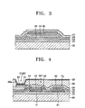
- FIG. 3 is a cross-sectional view illustrating a double capacitor according to a second exemplary embodiment of the present invention.
- FIG. 4 is a cross-sectional view illustrating a sub-pixel of an active matrix type organic electroluminescent display according to a third exemplary embodiment of the present invention.
- FIG. 5 is a cross-sectional view illustrating the sub-pixel of an active matrix type organic electroluminescent display according to a fourth exemplary embodiment of the present invention.
- FIG. 6 is a cross-sectional view illustrating the sub-pixel of an active matrix type organic electroluminescent display according to a fifth exemplary embodiment of the present invention.
- FIG. 2 illustrates a capacitor according to a first exemplary embodiment of the present invention.
- the capacitor comprises a first electrode and second electrode.
- "on" does not require physical contact. In other words, one layer formed on another may physically touch that layer or there may be additional layers between them.
- a buffer layer 21 is formed on a substrate 20, a first electrode 22 is formed on the buffer layer 21, a first insulating layer 23 is formed to cover the first electrode 22, a second electrode 24 is formed on the first insulating layer 23, and a second insulating layer 25 is formed to cover the second electrode 24.
- the substrate 20 may be formed of glass or plastic.
- the buffer layer 21 and the substrate 20 may form a single body.
- the substrate 20 may be formed of a P type silicon or an N type silicon.
- the buffer layer 21 may be omitted.
- the first electrode 22 and second electrode 24 may be formed of a conductive material such as metal, a semiconductor thin film, such as conductive polysilicon, a conductive polymer, or other like substances.
- the material of the first electrode 22 and second electrode 24 may be any material that can be used for a capacitor electrode in a semiconductor device or a flat panel display.
- the first insulating layer 23, interposed between the first electrode 22 and the second electrode 24, may be used as a dielectric layer, and it may be formed of SiO 2 , SiN x , or other like materials.
- the first electrode 22 may be formed to be larger than the second electrode 24. Also, the second electrode 24 may not overlap an edge portion of the first electrode 22.
- the second electrode 24 wiring may be disposed above an edge portion of the first electrode 22, and an electrode body of the second electrode 24 may be located at an area corresponding to the pattern of the first electrode 22.
- Forming the first electrode 22 and second electrode 24 as described above may prevent insulation destruction of the insulating layer 23. It also may prevent a current leakage at the edge portion of the first electrode 22 and a short circuit between the first electrode 22 and second electrode 24.
- FIG. 3 illustrates a double capacitor according to a second exemplary embodiment of the present invention.
- the second exemplary embodiment differs from the first exemplary embodiment in that a third electrode 26 is formed on the second insulating layer 25, and a third insulating layer 27 is formed on the third electrode 26.
- a first electrode 22, a first insulating layer 23, and a second electrode 24 form a first capacitor.
- the second electrode 24, a second insulating layer 25, and a third electrode 26 form a second capacitor.
- the second electrode 24 is greater than the third electrode 26.
- the third electrode 26 may be patterned within the pattern of the second electrode 24. Therefore, a current leakage, insulation destruction of the insulating layer 25, and a short circuit may be easily prevented.
- the capacitor as described above may be used in various semiconductor devices and flat panel displays, including liquid crystal displays, organic electroluminescent displays, and inorganic electroluminescent displays.
- FIG. 4 is a cross-sectional view illustrating a sub-pixel of an active type organic electroluminescent display according to a third exemplary embodiment of the present invention.
- the capacitor according to exemplary embodiments of the present invention may be applied not only as a storage capacitor in a sub-pixel, but it may also be used for different types of drivers.
- the organic electro luminescent display comprises a self-luminescent organic light emitting diode (OLED), at least one thin film transistor (TFT) connected to the OLED, and a storage capacitor Cst, as shown in FIG. 4.
- OLED organic light emitting diode
- TFT thin film transistor
- a buffer layer 31 may be formed on an insulating substrate 30, which may be formed of glass, and the thin film transistor TFT and the capacitor Cst are formed above the buffer layer 31.
- the buffer layer 31 may be formed of SiO 2 , and deposited to a thickness of about 3000 ⁇ using as a method such as plasma enhanced chemical vapor deposition (PECVD), atmospheric pressure chemical vapor deposition (APCVD), low pressure chemical vapor deposition (LPCVD), electron cyclotron resonance (ECR), or other like methods.
- PECVD plasma enhanced chemical vapor deposition
- APCVD atmospheric pressure chemical vapor deposition
- LPCVD low pressure chemical vapor deposition
- ECR electron cyclotron resonance
- the insulating substrate 30 may be formed of plastic, and in this case, the buffer layer 31 may be omitted.
- the thin film transistor TFT includes an active layer 41 formed on the buffer layer 31, a gate insulating layer 32 formed above the active layer 41, a gate electrode 42 formed above the gate insulating layer 32, and a source electrode 43 and a drain electrode 44 connected to the active layer 41.
- the active layer 41 may be formed of inorganic semiconductor or organic semiconductor material at a thickness of about 500 ⁇ .
- amorphous silicon may be formed and crystallized by various types of crystallization methods.
- the active layer 41 includes a source region and a drain region doped with high-density N-type or P-type impurities, and a channel region between the source region and the drain region.
- the inorganic semiconductor may include CdS, GaS, ZnS, CdSe, CaSe, ZnSe, CdTe, SiC, silicon, including amorphous silicon or polysilicon, or other like materials.
- the organic semiconductor may include a semiconductive organic material having a band gap of 1ev through 4ev.
- the semiconductive organic material may include a polymer and a monomer. Examples of the monomer include polythiophene and its derivative, polyparaphenylenevenylene and its derivative, polyparaphenylene and its derivative, polyfluorene and its derivative, polythiophenevinylene and its derivative, polythiophene-Heterocyclic Aromatic Co and its derivative, and other like substances.
- polymer examples include pentacene, tetracene, oligoacene of naphthalene, and their derivatives, alpha-6-thiophene, oligothiophene of alpha-5-thiophene, and their derivatives, phthalocyanines with or without metal, and their derivatives, pyromellitic dianhydride or pyromellitic diimide, and their derivatives, perylenetetracarbocxylic acid dianhydride or perylenetetracarboxylic acid diimide and their derivatives, and other like substances.
- the gate insulating layer 32 may be formed of SiO 2 , and a gate electrode 42 may be formed as a conductive metal layer of MoW, Al, Cr, or Al/Cu. Other conductive materials, including a conductive polymer, may be used for the gate electrode 42.
- the gate electrode 42 is coupled to a gate line applying TFT on/off signals, and a region of the gate electrode 42 corresponds to a channel region of the active layer 41.
- An inter-insulating layer 33, above the gate electrode 42, may be formed of SiO 2 , SiN x or other like substances.
- the source electrode 43 and the drain electrode 44 are formed above the inter-insulating layer 33, and contact holes are punched in the inter-insulating layer 33 and gate insulating layer 32.
- the source and drain electrodes 43 and 44 may be formed of a conductive metal layer such as MoW, Al, Cr, or Al/Cu, and a conductive polymer.
- a passivation layer 34 which may be formed of SiN x , is formed above the source and drain electrodes 43 and 44, and a pixel-definition layer 35, which may be formed of acryl or polyimid, is formed above the passivation layer 34.
- the thin film transistor TFT is not restricted to the above structure. It may have various structures of a conventional thin film transistor.
- the drain electrode 44 is coupled to an anode electrode 51 of the organic light emitting diode OLED.
- the anode electrode 51 is formed above the passivation layer 34, and the pixel-definition layer 35 is formed above the anode electrode 51.
- An opening 35a may be formed in the pixel-definition layer 35, and the organic light emitting diode OLED is formed therein.
- the organic light emitting diode OLED displays images by emitting red, green, and blue light in accordance with the flow of current.
- the organic light emitting diode OLED is comprised of the anode electrode 51, a cathode electrode 53, and an organic light emitting layer 52 interposed between them
- the anode electrode 51 may be coupled to the drain electrode 44, and the cathode electrode 53 may be formed to cover all pixels of the active matrix type organic electroluminescent display.
- the anode electrode 51 may be formed of a transparent electrode like ITO, or of a reflex type electrode such as Al/ITO. With a rear emitting display, the cathode electrode 53 may be formed of Al/Ca, and with a front emitting display, it may be formed of a transparent electrode such as Mg-Ag/ITO. The positions of the anode electrode 51 and the cathode electrode 53 may be interchanged.
- the organic light emitting layer 52 may be formed of a low molecular organic layer or a high molecular organic layer.
- a Hole Injection Layer HIL
- HTL Hole Transport Layer
- EML Emission Layer
- ETL Electron Transport Layer
- EIL Electron Injection Layer
- CuPc Copper phthalocyanine
- N, N'-Di(naphthalene-1-yl)-N, N'-diphenyl-benzidine NPB, tris-8-hydroxyquinoline aluminum Alq3, or other like substances may be used as the low polymer layer.
- the low polymer layers as described above may be formed by vacuum deposition.
- the high molecular layer may have a structure including an HTL and an EML.
- the HTL may be formed of PEDOT
- the EML may be formed of poly-phenylenevinylene PPV and polyfluorene. Screen printing or ink jet printing may be used to form these layers.
- the structure of the organic light emitting diode is not restricted to the above.
- the capacitor Cst includes a first electrode 61 formed above the buffer layer 31, and a second electrode 62 formed above the first electrode 61.
- the gate insulating layer 32 is interposed between the first electrode 61 and second electrode 62.
- the first electrode 61 may be formed of the same material as the active layer 41, and the second electrode 62 may be formed of the same material as the gate electrode 42.
- the first electrode 61 and second electrode 62 may be formed simultaneously with the active layer 41 and gate electrode 42, respectively.
- the first electrode 61 may be connected to a driving power line Vdd, and the second electrode 62 may be connected to the source electrode of TFT, but this configuration is not restricted to the above description.
- the second electrode 62 may be formed smaller than the first electrode 61, and an edge portion of the first electrode 61 may not overlap with the second electrode 62.
- the second electrode 62 may be located within the pattern of the first electrode 61.
- the edge portion of the first electrode 61 does not overlap the second electrode 62, the insulation destruction of the gate insulating layer 32, current leakage and a short-circuit occurring at the edge portion of the first electrode 61 may be prevented.
- the active layer 41 and the first electrode 61 are formed of polysilicon, a surface with a higher roughness and a larger step may be formed. Therefore, the method described above is useful to solve the problems of current leakage, destruction of the insulating layer, and short-circuiting of capacitor electrodes.
- the structure of the capacitor of the fourth exemplary embodiment of the present invention may be applied to a double capacitor in which a third electrode 63 is formed of the same material as the source and drain electrodes 43 and 44 of the thin film transistor TFT.
- the third electrode 63 is smaller than the second electrode 62 in that the pattern of the third electrode 63 corresponds to an area within the pattern of the second electrode 62, so that an edge portion of the third electrode 63 does not overlap the second electrode 62.
- the structure of the capacitor, of the fifth exemplary embodiment of the present invention, as shown in FIG. 6, may be applied to a capacitor formed with only the second electrode 62 and the third electrode 63.
- the fifth embodiment does not have a first electrode 61.
- the third electrode 63 is smaller than the second electrode 62in that the pattern of the third electrode 63 corresponds to an area within the pattern of the second electrode 62, so that edge portion of the second electrode 62 is not under the third electrode 63.
- Exemplary embodiments of the present invention may be also applied to liquid crystal displays and inorganic electroluminescent displays.
- the insulation destruction of a thin insulating layer near the step of the lower electrode may be prevented.
Landscapes
- Devices For Indicating Variable Information By Combining Individual Elements (AREA)
- Electroluminescent Light Sources (AREA)
- Semiconductor Integrated Circuits (AREA)
- Metal-Oxide And Bipolar Metal-Oxide Semiconductor Integrated Circuits (AREA)
- Thin Film Transistor (AREA)
Abstract
Description
- This application claims the benefit of Korean Patent Application No. 2003-84880, filed on November 27, 2003, which is hereby incorporated by reference for all purposes as if fully set forth herein.
- The present invention relates to a capacitor and a flat panel display having the capacitor, and more particularly, to a capacitor with an improved electrode structure and a flat panel display including the same.
- Passive elements, such as resistors and capacitors, and active elements, such as thin film transistors (TFTs), diodes, and metal oxide semiconductor field effect transistors (MOSFETs), are used in integrated circuits and flat panel displays.
- Large capacity capacitors may be required to manufacture an integrated circuit with high integration density that operates at high speed. In the case of flat panel displays, such as liquid crystal displays, organic light emitting displays, and inorganic light emitting displays, a plurality of storage capacitors may be formed to correspond to one pixel, thereby improving the display's picture quality. Storage capacitors store data signals during a predetermined time frame.
- FIG. 1 illustrates a conventional capacitor that generally may be used in a semiconductor device or a flat panel display. The capacitor includes a sequentially formed
substrate 10, a buffer layer 11, alower electrode 12, aninsulating layer 13 covering thelower electrode 12, and anupper electrode 14 overlapping thelower electrode 12. - In a capacitor with the above structure, the
upper electrode 14 is formed wider than thelower electrode 12 due to a process margin for patterning and a wiring structure plan. Specifically, when a mask align operation is performed using an exposure unit to pattern theupper electrode 14, a process margin is formed on theupper electrode 14 to compensate for an exposure unit align error. Also, by considering the process margin, the plan of a through hole for connecting a data line and the wiring structure of theupper electrode 14 is easily laid out. - However, referring to FIG. 1, when the
upper electrode 14 is formed wider than thelower electrode 12, theinsulating layer 13 relatively thin at an edge portion S of thelower electrode 12, which may permit current leakage. Current leakage may destroy insulation between the upper andlower electrodes - A TFT used in a flat panel display generally employs polysilicon active layers to achieve a high response speed and dynamic display images. With a front emitting type display, increasing the number of TFTs per pixel may improve the aperture ratio. In this case, a polysilicon active layer may be used as the capacitor's
lower electrode 12. - However, when polysilicon is used as the
lower electrode 12, current leakage may increase because polysilicon is typically rougher than a metal used to manufacture thelower electrode 12. Therefore, deterioration of theinsulating layer 13 at the relatively thin edge portion S may become very problematic. - The present invention provides a capacitor that may be capable of preventing current leakage, insulation destruction, and short circuits generated at the step of a lower electrode.
- The present invention also provides a flat panel display including the capacitor.
- Additional features of the invention will be set forth in the description which follows, and in part will be apparent from the description, or may be learned by practice of the invention.
- The present invention discloses a capacitor, comprising at least two electrodes, disposed in a stacked structure, that are insulated from each other, wherein each electrode is smaller than a lower electrode.
- The present invention also discloses a capacitor, comprising at least two electrodes, disposed in a stacked structure, that are insulated from each other, wherein each electrode does not overlap an edge portion of a lower electrode.
- The present invention also discloses a flat panel display, comprising a light emitting device, a thin film transistor and a capacitor. Each thin film transistor has a semiconductor thin film, a gate electrode insulated from the semiconductor thin film, and source and drain electrodes coupled to the semiconductor thin film. The capacitor has at least two electrodes, disposed in a stacked structure, that are insulated from each other. Each electrode of the capacitor is smaller than a lower electrode of the capacitor.
- The present invention also discloses a flat panel display, comprising a light emitting device, a thin film transistor and a capacitor. The thin film transistor has a semiconductor thin film, a gate electrode that is insulated from the semiconductor thin film, a source electrode and a drain electrode coupled to the semiconductor thin film. The capacitor has at least two electrodes, disposed in a stacked structure, that are insulated from each other. Each electrode of the capacitor does not overlap an edge portion of a lower electrode of the capacitor.
- It is to be understood that both the foregoing general description and the following detailed description are exemplary and explanatory and are intended to provide further explanation of the invention as claimed.
- The accompanying drawings, which are included to provide a further understanding of the invention and are incorporated in and constitute a part of this specification, illustrate embodiments of the invention and together with the description serve to explain the principles of the invention.
- FIG. 1 is a cross-sectional view of a conventional capacitor showing an edge portion of a lower electrode.
- FIG. 2 is a cross-sectional view illustrating a capacitor according to a first exemplary embodiment of the present invention.
- FIG. 3 is a cross-sectional view illustrating a double capacitor according to a second exemplary embodiment of the present invention.
- FIG. 4 is a cross-sectional view illustrating a sub-pixel of an active matrix type organic electroluminescent display according to a third exemplary embodiment of the present invention.
- FIG. 5 is a cross-sectional view illustrating the sub-pixel of an active matrix type organic electroluminescent display according to a fourth exemplary embodiment of the present invention.
- FIG. 6 is a cross-sectional view illustrating the sub-pixel of an active matrix type organic electroluminescent display according to a fifth exemplary embodiment of the present invention.
- FIG. 2 illustrates a capacitor according to a first exemplary embodiment of the present invention. The capacitor comprises a first electrode and second electrode. In exemplary embodiments of the present invention, "on" does not require physical contact. In other words, one layer formed on another may physically touch that layer or there may be additional layers between them.
- A
buffer layer 21 is formed on asubstrate 20, afirst electrode 22 is formed on thebuffer layer 21, a firstinsulating layer 23 is formed to cover thefirst electrode 22, asecond electrode 24 is formed on the firstinsulating layer 23, and a secondinsulating layer 25 is formed to cover thesecond electrode 24. - With a flat panel display, the
substrate 20 may be formed of glass or plastic. Thebuffer layer 21 and thesubstrate 20 may form a single body. - On the other hand, with a semiconductor device, the
substrate 20 may be formed of a P type silicon or an N type silicon. In this case, thebuffer layer 21 may be omitted. - The
first electrode 22 andsecond electrode 24 may be formed of a conductive material such as metal, a semiconductor thin film, such as conductive polysilicon, a conductive polymer, or other like substances. The material of thefirst electrode 22 andsecond electrode 24 may be any material that can be used for a capacitor electrode in a semiconductor device or a flat panel display. - The first
insulating layer 23, interposed between thefirst electrode 22 and thesecond electrode 24, may be used as a dielectric layer, and it may be formed of SiO2, SiNx, or other like materials. - The
first electrode 22 may be formed to be larger than thesecond electrode 24. Also, thesecond electrode 24 may not overlap an edge portion of thefirst electrode 22. Thesecond electrode 24 wiring may be disposed above an edge portion of thefirst electrode 22, and an electrode body of thesecond electrode 24 may be located at an area corresponding to the pattern of thefirst electrode 22. - Forming the
first electrode 22 andsecond electrode 24 as described above may prevent insulation destruction of theinsulating layer 23. It also may prevent a current leakage at the edge portion of thefirst electrode 22 and a short circuit between thefirst electrode 22 andsecond electrode 24. - FIG. 3 illustrates a double capacitor according to a second exemplary embodiment of the present invention.
- The second exemplary embodiment differs from the first exemplary embodiment in that a
third electrode 26 is formed on the secondinsulating layer 25, and a thirdinsulating layer 27 is formed on thethird electrode 26. Afirst electrode 22, a firstinsulating layer 23, and asecond electrode 24 form a first capacitor. Thesecond electrode 24, a secondinsulating layer 25, and athird electrode 26 form a second capacitor. - In the second exemplary embodiment, the
second electrode 24 is greater than thethird electrode 26. Thethird electrode 26 may be patterned within the pattern of thesecond electrode 24. Therefore, a current leakage, insulation destruction of the insulatinglayer 25, and a short circuit may be easily prevented. - The capacitor as described above may be used in various semiconductor devices and flat panel displays, including liquid crystal displays, organic electroluminescent displays, and inorganic electroluminescent displays.
- FIG. 4 is a cross-sectional view illustrating a sub-pixel of an active type organic electroluminescent display according to a third exemplary embodiment of the present invention. The capacitor according to exemplary embodiments of the present invention may be applied not only as a storage capacitor in a sub-pixel, but it may also be used for different types of drivers.
- The organic electro luminescent display comprises a self-luminescent organic light emitting diode (OLED), at least one thin film transistor (TFT) connected to the OLED, and a storage capacitor Cst, as shown in FIG. 4.
- Referring to FIG. 4, a
buffer layer 31 may be formed on an insulatingsubstrate 30, which may be formed of glass, and the thin film transistor TFT and the capacitor Cst are formed above thebuffer layer 31. Thebuffer layer 31 may be formed of SiO2, and deposited to a thickness of about 3000Å using as a method such as plasma enhanced chemical vapor deposition (PECVD), atmospheric pressure chemical vapor deposition (APCVD), low pressure chemical vapor deposition (LPCVD), electron cyclotron resonance (ECR), or other like methods. The insulatingsubstrate 30 may be formed of plastic, and in this case, thebuffer layer 31 may be omitted. - The thin film transistor TFT includes an
active layer 41 formed on thebuffer layer 31, agate insulating layer 32 formed above theactive layer 41, agate electrode 42 formed above thegate insulating layer 32, and asource electrode 43 and adrain electrode 44 connected to theactive layer 41. - The
active layer 41 may be formed of inorganic semiconductor or organic semiconductor material at a thickness of about 500Å. When theactive layer 41 is formed of a polysilicon inorganic semiconductor, amorphous silicon may be formed and crystallized by various types of crystallization methods. Theactive layer 41 includes a source region and a drain region doped with high-density N-type or P-type impurities, and a channel region between the source region and the drain region. - The inorganic semiconductor may include CdS, GaS, ZnS, CdSe, CaSe, ZnSe, CdTe, SiC, silicon, including amorphous silicon or polysilicon, or other like materials.
- The organic semiconductor may include a semiconductive organic material having a band gap of 1ev through 4ev. The semiconductive organic material may include a polymer and a monomer. Examples of the monomer include polythiophene and its derivative, polyparaphenylenevenylene and its derivative, polyparaphenylene and its derivative, polyfluorene and its derivative, polythiophenevinylene and its derivative, polythiophene-Heterocyclic Aromatic Co and its derivative, and other like substances. Examples of the polymer include pentacene, tetracene, oligoacene of naphthalene, and their derivatives, alpha-6-thiophene, oligothiophene of alpha-5-thiophene, and their derivatives, phthalocyanines with or without metal, and their derivatives, pyromellitic dianhydride or pyromellitic diimide, and their derivatives, perylenetetracarbocxylic acid dianhydride or perylenetetracarboxylic acid diimide and their derivatives, and other like substances.
- The
gate insulating layer 32 may be formed of SiO2, and agate electrode 42 may be formed as a conductive metal layer of MoW, Al, Cr, or Al/Cu. Other conductive materials, including a conductive polymer, may be used for thegate electrode 42. Thegate electrode 42 is coupled to a gate line applying TFT on/off signals, and a region of thegate electrode 42 corresponds to a channel region of theactive layer 41. - An
inter-insulating layer 33, above thegate electrode 42, may be formed of SiO2, SiNx or other like substances. Thesource electrode 43 and thedrain electrode 44 are formed above theinter-insulating layer 33, and contact holes are punched in theinter-insulating layer 33 andgate insulating layer 32. The source and drainelectrodes - A
passivation layer 34, which may be formed of SiNx, is formed above the source and drainelectrodes definition layer 35, which may be formed of acryl or polyimid, is formed above thepassivation layer 34. - The thin film transistor TFT is not restricted to the above structure. It may have various structures of a conventional thin film transistor.
- The
drain electrode 44 is coupled to ananode electrode 51 of the organic light emitting diode OLED. Theanode electrode 51 is formed above thepassivation layer 34, and the pixel-definition layer 35 is formed above theanode electrode 51. Anopening 35a may be formed in the pixel-definition layer 35, and the organic light emitting diode OLED is formed therein. - The organic light emitting diode OLED displays images by emitting red, green, and blue light in accordance with the flow of current. The organic light emitting diode OLED is comprised of the
anode electrode 51, acathode electrode 53, and an organiclight emitting layer 52 interposed between them Theanode electrode 51 may be coupled to thedrain electrode 44, and thecathode electrode 53 may be formed to cover all pixels of the active matrix type organic electroluminescent display. - The
anode electrode 51 may be formed of a transparent electrode like ITO, or of a reflex type electrode such as Al/ITO. With a rear emitting display, thecathode electrode 53 may be formed of Al/Ca, and with a front emitting display, it may be formed of a transparent electrode such as Mg-Ag/ITO. The positions of theanode electrode 51 and thecathode electrode 53 may be interchanged. - The organic
light emitting layer 52 may be formed of a low molecular organic layer or a high molecular organic layer. - When the low molecular organic layer is used, a Hole Injection Layer (HIL), a Hole Transport Layer (HTL), an Emission Layer (EML), an Electron Transport Layer (ETL), and an Electron Injection Layer (EIL) may be deposited and formed in a single layer structure or in a multiple layer structure. Copper phthalocyanine CuPc, N, N'-Di(naphthalene-1-yl)-N, N'-diphenyl-benzidine NPB, tris-8-hydroxyquinoline aluminum Alq3, or other like substances may be used as the low polymer layer. The low polymer layers as described above may be formed by vacuum deposition.
- The high molecular layer may have a structure including an HTL and an EML. In this case, the HTL may be formed of PEDOT, and the EML may be formed of poly-phenylenevinylene PPV and polyfluorene. Screen printing or ink jet printing may be used to form these layers.
- The structure of the organic light emitting diode is not restricted to the above.
- The capacitor Cst includes a
first electrode 61 formed above thebuffer layer 31, and asecond electrode 62 formed above thefirst electrode 61. Thegate insulating layer 32 is interposed between thefirst electrode 61 andsecond electrode 62. - In accordance with an exemplary embodiment of the present invention, the
first electrode 61 may be formed of the same material as theactive layer 41, and thesecond electrode 62 may be formed of the same material as thegate electrode 42. Thefirst electrode 61 andsecond electrode 62 may be formed simultaneously with theactive layer 41 andgate electrode 42, respectively. Thefirst electrode 61 may be connected to a driving power line Vdd, and thesecond electrode 62 may be connected to the source electrode of TFT, but this configuration is not restricted to the above description. - In this case, the
second electrode 62 may be formed smaller than thefirst electrode 61, and an edge portion of thefirst electrode 61 may not overlap with thesecond electrode 62. Thesecond electrode 62 may be located within the pattern of thefirst electrode 61. - Since the edge portion of the
first electrode 61 does not overlap thesecond electrode 62, the insulation destruction of thegate insulating layer 32, current leakage and a short-circuit occurring at the edge portion of thefirst electrode 61 may be prevented. - Referring to FIG. 4, when the
active layer 41 and thefirst electrode 61 are formed of polysilicon, a surface with a higher roughness and a larger step may be formed. Therefore, the method described above is useful to solve the problems of current leakage, destruction of the insulating layer, and short-circuiting of capacitor electrodes. - The structure of the capacitor of the fourth exemplary embodiment of the present invention, as shown in FIG. 5, may be applied to a double capacitor in which a
third electrode 63 is formed of the same material as the source and drainelectrodes third electrode 63 is smaller than thesecond electrode 62 in that the pattern of thethird electrode 63 corresponds to an area within the pattern of thesecond electrode 62, so that an edge portion of thethird electrode 63 does not overlap thesecond electrode 62. - The structure of the capacitor, of the fifth exemplary embodiment of the present invention, as shown in FIG. 6, may be applied to a capacitor formed with only the
second electrode 62 and thethird electrode 63. Unlike the fourth embodiment, the fifth embodiment does not have afirst electrode 61. Referring to FIG. 6, similar to the fourth embodiment, thethird electrode 63 is smaller than the second electrode 62in that the pattern of thethird electrode 63 corresponds to an area within the pattern of thesecond electrode 62, so that edge portion of thesecond electrode 62 is not under thethird electrode 63. As such, problems of current leakage, destruction of the insulating layer, and short-circuit may be solved. - Exemplary embodiments of the present invention may be also applied to liquid crystal displays and inorganic electroluminescent displays.
- As described above, according to exemplary embodiments of the present invention, the following effects are obtained.
- First, current leakage caused by a thin insulating layer in a portion corresponding to a step of a lower electrode may be solved.
- Second, the insulation destruction of a thin insulating layer near the step of the lower electrode may be prevented.
- Third, a short-circuit between an upper electrode and a lower electrode caused by the insulation destruction of the insulating layer or racking of the insulating layer, may be prevented.
- It will be apparent to those skilled in the art that various modifications and variation can be made in the present invention without departing from the spirit or scope of the invention. Thus, it is intended that the present invention cover the modifications and variations of this invention provided they come within the scope of the appended claims and their equivalents.
Claims (20)
- A capacitor, comprising:wherein each electrode is smaller than a lower electrode.at least two electrodes, disposed in a stacked structure, that are insulated from each other,
- The capacitor of claim 1, wherein at least one electrode is a semiconductor thin film.
- The capacitor of claim 2, wherein the semiconductor thin film is formed of polysilicon.
- The capacitor of claim 1, wherein at least one electrode is formed of a metal.
- The capacitor of claim 1, wherein at least one electrode is formed of a conductive polymer.
- A capacitor, comprising:wherein each electrode does not overlap an edge portion of a lower electrode.at least two electrodes, disposed in a stacked structure, that are insulated from each other,
- The capacitor of claim 6, wherein at least one electrode is a semiconductor thin film.
- The capacitor of claim 7, wherein the semiconductor thin film is formed of polysilicon.
- The capacitor of claim 6, wherein at least one electrode is formed of a metal.
- The capacitor of claim 6, wherein at least one electrode is formed of a conductive polymer.
- A flat panel display, comprising:wherein each electrode of the capacitor is smaller than a lower electrode of the capacitor.a light emitting device;a thin film transistor, coupled to the light emitting device, further comprising:a semiconductor thin film;a gate electrode insulated from the semiconductor thin film;a source electrode coupled to the semiconductor thin film; and
a drain electrode coupled to the semiconductor thin film; anda capacitor having at least two electrodes, disposed in a stacked structure and insulated from each other; - The flat panel display of claim 11, wherein a capacitor electrode is formed of a same material as the semiconductor thin film.
- The flat panel display of claim 12, wherein the capacitor electrode and the semiconductor thin film are formed of polysilicon.
- The flat panel display of claim 11, wherein a capacitor electrode is formed of a same material as the gate electrode.
- The flat panel display of claim 11, wherein a capacitor electrode is formed of a same material as the source electrode and the drain electrode.
- A flat panel display, comprising:wherein each electrode of the capacitor does not overlap an edge portion of a lower electrode of the capacitor.a light emitting device;a thin film transistor, coupled to the light emitting device, further comprising:a semiconductor thin film;a gate electrode that is insulated from the semiconductor thin film;a source electrode coupled to the semiconductor thin film; anda drain electrode coupled to the semiconductor thin film; anda capacitor having at least two electrodes, disposed in a stacked structure and insulated from each other,
- The flat panel display of claim 16, wherein a capacitor electrode is formed of a same material as the semiconductor thin film.
- The flat panel display of claim 17, wherein the capacitor electrode and the semiconductor thin film are formed of polysilicon.
- The flat panel display of claim 16, wherein a capacitor electrode is formed of a same material as the gate electrode.
- The flat panel display of claim 16, wherein a capacitor electrode is formed of a same material as the source electrode and the drain electrode.
Applications Claiming Priority (2)
| Application Number | Priority Date | Filing Date | Title |
|---|---|---|---|
| KR1020030084880A KR20050051140A (en) | 2003-11-27 | 2003-11-27 | Capacitor and flat panel display therewith |
| KR2003084880 | 2003-11-27 |
Publications (1)
| Publication Number | Publication Date |
|---|---|
| EP1536485A1 true EP1536485A1 (en) | 2005-06-01 |
Family
ID=34464757
Family Applications (1)
| Application Number | Title | Priority Date | Filing Date |
|---|---|---|---|
| EP04090468A Withdrawn EP1536485A1 (en) | 2003-11-27 | 2004-11-26 | Capacitor and flat panel display having the same |
Country Status (5)
| Country | Link |
|---|---|
| US (1) | US20050121677A1 (en) |
| EP (1) | EP1536485A1 (en) |
| JP (1) | JP2005159290A (en) |
| KR (1) | KR20050051140A (en) |
| CN (1) | CN1622240A (en) |
Cited By (1)
| Publication number | Priority date | Publication date | Assignee | Title |
|---|---|---|---|---|
| US12027535B2 (en) | 2014-07-24 | 2024-07-02 | Semiconductor Energy Laboratory Co., Ltd. | Semiconductor device with a capacitor and a plurality of overlapping openings in the conductive layers |
Families Citing this family (15)
| Publication number | Priority date | Publication date | Assignee | Title |
|---|---|---|---|---|
| KR100700659B1 (en) * | 2005-03-29 | 2007-03-27 | 삼성에스디아이 주식회사 | Organic light emitting display device and manufacturing method |
| US20060226429A1 (en) * | 2005-04-08 | 2006-10-12 | Sigalas Mihail M | Method and apparatus for directional organic light emitting diodes |
| US7888702B2 (en) * | 2005-04-15 | 2011-02-15 | Semiconductor Energy Laboratory Co., Ltd. | Display device and manufacturing method of the display device |
| KR100719707B1 (en) * | 2005-08-30 | 2007-05-17 | 삼성에스디아이 주식회사 | OLED display device and manufacturing method thereof |
| JP4934599B2 (en) * | 2007-01-29 | 2012-05-16 | キヤノン株式会社 | Active matrix display device |
| KR100864886B1 (en) * | 2007-03-28 | 2008-10-22 | 삼성에스디아이 주식회사 | Flat panel display and manufacturing method |
| JP2008282903A (en) | 2007-05-09 | 2008-11-20 | Nec Electronics Corp | Semiconductor device and manufacturing method thereof |
| JP2010283072A (en) * | 2009-06-03 | 2010-12-16 | Sumitomo Chemical Co Ltd | Organic thin film transistor, planar light source and display device |
| WO2011138743A1 (en) * | 2010-05-06 | 2011-11-10 | Basf Se | Use of pyromellitic diimides in organic electronics and organic photovoltaics |
| KR101482627B1 (en) | 2010-06-07 | 2015-01-14 | 삼성디스플레이 주식회사 | Flat display device and Method for manufacturing the same |
| KR102028025B1 (en) * | 2012-11-13 | 2019-10-04 | 삼성디스플레이 주식회사 | Organic light emitting display apparatus and method of manufacturing the same |
| KR102490881B1 (en) * | 2014-12-26 | 2023-01-25 | 삼성디스플레이 주식회사 | Organic light emitting display device and manufacturing method of the same |
| CN105140305B (en) * | 2015-09-08 | 2016-09-28 | 福建省福芯电子科技有限公司 | High-pressure flat plate electric capacity and demagnetization sample circuit |
| KR102460748B1 (en) * | 2017-09-21 | 2022-10-31 | 삼성전기주식회사 | Capacitor Component |
| CN209000913U (en) * | 2018-11-06 | 2019-06-18 | 惠科股份有限公司 | A display panel and display device |
Citations (4)
| Publication number | Priority date | Publication date | Assignee | Title |
|---|---|---|---|---|
| US4914546A (en) * | 1989-02-03 | 1990-04-03 | Micrel Incorporated | Stacked multi-polysilicon layer capacitor |
| US4943471A (en) * | 1986-05-20 | 1990-07-24 | Kanegafuchi Kagaku Kogyo Kabushiki Kaisha | Patterned thin film and process for preparing the same |
| US20030122127A1 (en) * | 1999-07-07 | 2003-07-03 | Hiroaki Yonekura | Thin film transistor array and its manufacturing method |
| US20030186489A1 (en) * | 2002-03-26 | 2003-10-02 | Semiconductor Energy Laboratory Co., Ltd. | Semiconductor device and method for preparing the same |
Family Cites Families (12)
| Publication number | Priority date | Publication date | Assignee | Title |
|---|---|---|---|---|
| JP4179483B2 (en) * | 1996-02-13 | 2008-11-12 | 株式会社半導体エネルギー研究所 | Method for manufacturing display device |
| TW347558B (en) * | 1996-07-10 | 1998-12-11 | Fujitsu Ltd | Semiconductor device with self-aligned contact and its manufacture |
| TW377495B (en) * | 1996-10-04 | 1999-12-21 | Hitachi Ltd | Method of manufacturing semiconductor memory cells and the same apparatus |
| JP3784491B2 (en) * | 1997-03-28 | 2006-06-14 | 株式会社半導体エネルギー研究所 | Active matrix display device |
| JP2000058783A (en) * | 1998-08-06 | 2000-02-25 | Mitsubishi Electric Corp | Semiconductor device and method of manufacturing the same |
| US6512504B1 (en) * | 1999-04-27 | 2003-01-28 | Semiconductor Energy Laborayory Co., Ltd. | Electronic device and electronic apparatus |
| TW472384B (en) * | 1999-06-17 | 2002-01-11 | Fujitsu Ltd | Semiconductor device and method of manufacturing the same |
| KR100404225B1 (en) * | 2000-12-28 | 2003-11-01 | 엘지.필립스 엘시디 주식회사 | Liquid crystal display device and method for manufacturing the same |
| TW575777B (en) * | 2001-03-30 | 2004-02-11 | Sanyo Electric Co | Active matrix type display device |
| KR100838185B1 (en) * | 2001-09-24 | 2008-06-13 | 엘지디스플레이 주식회사 | Array substrate, liquid crystal display device using same, and manufacturing method thereof |
| TW516239B (en) * | 2001-11-01 | 2003-01-01 | Chi Mei Optoelectronics Corp | Pixel structure with storage capacitor, fabrication method for the same, and liquid crystal display device |
| JP3891846B2 (en) * | 2002-01-15 | 2007-03-14 | 株式会社日立製作所 | Liquid crystal display |
-
2003
- 2003-11-27 KR KR1020030084880A patent/KR20050051140A/en not_active Ceased
-
2004
- 2004-08-02 JP JP2004226120A patent/JP2005159290A/en active Pending
- 2004-11-17 US US10/989,645 patent/US20050121677A1/en not_active Abandoned
- 2004-11-26 EP EP04090468A patent/EP1536485A1/en not_active Withdrawn
- 2004-11-26 CN CNA2004100958799A patent/CN1622240A/en active Pending
Patent Citations (4)
| Publication number | Priority date | Publication date | Assignee | Title |
|---|---|---|---|---|
| US4943471A (en) * | 1986-05-20 | 1990-07-24 | Kanegafuchi Kagaku Kogyo Kabushiki Kaisha | Patterned thin film and process for preparing the same |
| US4914546A (en) * | 1989-02-03 | 1990-04-03 | Micrel Incorporated | Stacked multi-polysilicon layer capacitor |
| US20030122127A1 (en) * | 1999-07-07 | 2003-07-03 | Hiroaki Yonekura | Thin film transistor array and its manufacturing method |
| US20030186489A1 (en) * | 2002-03-26 | 2003-10-02 | Semiconductor Energy Laboratory Co., Ltd. | Semiconductor device and method for preparing the same |
Cited By (1)
| Publication number | Priority date | Publication date | Assignee | Title |
|---|---|---|---|---|
| US12027535B2 (en) | 2014-07-24 | 2024-07-02 | Semiconductor Energy Laboratory Co., Ltd. | Semiconductor device with a capacitor and a plurality of overlapping openings in the conductive layers |
Also Published As
| Publication number | Publication date |
|---|---|
| US20050121677A1 (en) | 2005-06-09 |
| KR20050051140A (en) | 2005-06-01 |
| JP2005159290A (en) | 2005-06-16 |
| CN1622240A (en) | 2005-06-01 |
Similar Documents
| Publication | Publication Date | Title |
|---|---|---|
| JP5436516B2 (en) | ORGANIC THIN FILM TRANSISTOR AND FLAT DISPLAY DEVICE HAVING THE SAME | |
| US7652291B2 (en) | Flat panel display | |
| KR100683766B1 (en) | Flat panel display and manufacturing method | |
| US8324612B2 (en) | Thin film transistor, method of fabricating the same, and flat panel display having the same | |
| US7442960B2 (en) | TFT, method of manufacturing the TFT, flat panel display having the TFT, and method of manufacturing the flat panel display | |
| KR100553745B1 (en) | Flat Panel Display | |
| KR100647599B1 (en) | Organic electroluminescent display and manufacturing method thereof | |
| US20210296416A1 (en) | Organic light-emitting display apparatus and method of manufacturing the same | |
| KR20050090259A (en) | Flat display device | |
| KR20050113517A (en) | Electrolumimescence display device and method for manufacturing the same | |
| KR20050110905A (en) | Flat panel display device | |
| US20050121677A1 (en) | Capacitor and flat panel display having the same | |
| CN103681746A (en) | Organic light-emitting display apparatus and method of manufacturing the same | |
| KR100696522B1 (en) | Flat Panel Display | |
| JP4358152B2 (en) | Thin film transistor and flat panel display having the same | |
| US20050269562A1 (en) | Thin film transistor (TFT) and flat display panel having the thin film transistor (TFT) | |
| US7550766B2 (en) | Thin film transistor (TFT) and flat panel display including the TFT | |
| US20070290196A1 (en) | Organic light emitting display device and method for manufacturing the organic light emitting display device | |
| US20070158648A1 (en) | Organic thin film transistor and method of manufacturing the same | |
| KR100683665B1 (en) | Organic electroluminescent display | |
| KR100696525B1 (en) | Flat Panel Display | |
| KR100669702B1 (en) | Thin film transistor and flat panel display device having same | |
| KR101137382B1 (en) | Flat panel display apparatus | |
| KR100730222B1 (en) | Flat panel display device | |
| KR20050077832A (en) | Tft and flat panel display therewith |
Legal Events
| Date | Code | Title | Description |
|---|---|---|---|
| PUAI | Public reference made under article 153(3) epc to a published international application that has entered the european phase |
Free format text: ORIGINAL CODE: 0009012 |
|
| 17P | Request for examination filed |
Effective date: 20041126 |
|
| AK | Designated contracting states |
Kind code of ref document: A1 Designated state(s): AT BE BG CH CY CZ DE DK EE ES FI FR GB GR HU IE IS IT LI LU MC NL PL PT RO SE SI SK TR |
|
| AX | Request for extension of the european patent |
Extension state: AL HR LT LV MK YU |
|
| AKX | Designation fees paid |
Designated state(s): AT BE BG CH CY CZ DE DK EE ES FI FR GB GR HU IE IS IT LI LU MC NL PL PT RO SE SI SK TR |
|
| 17Q | First examination report despatched |
Effective date: 20060502 |
|
| STAA | Information on the status of an ep patent application or granted ep patent |
Free format text: STATUS: THE APPLICATION IS DEEMED TO BE WITHDRAWN |
|
| 18D | Application deemed to be withdrawn |
Effective date: 20070501 |