EP1536428A1 - Synchronizing method and synchronizing apparatus - Google Patents
Synchronizing method and synchronizing apparatus Download PDFInfo
- Publication number
- EP1536428A1 EP1536428A1 EP04021247A EP04021247A EP1536428A1 EP 1536428 A1 EP1536428 A1 EP 1536428A1 EP 04021247 A EP04021247 A EP 04021247A EP 04021247 A EP04021247 A EP 04021247A EP 1536428 A1 EP1536428 A1 EP 1536428A1
- Authority
- EP
- European Patent Office
- Prior art keywords
- period counter
- unit
- detection signal
- wdu
- synchronizing
- Prior art date
- Legal status (The legal status is an assumption and is not a legal conclusion. Google has not performed a legal analysis and makes no representation as to the accuracy of the status listed.)
- Withdrawn
Links
- 238000000034 method Methods 0.000 title claims description 33
- 238000001514 detection method Methods 0.000 claims abstract description 97
- 230000005540 biological transmission Effects 0.000 claims description 104
- 238000005070 sampling Methods 0.000 abstract 1
- 238000010586 diagram Methods 0.000 description 19
- 230000003287 optical effect Effects 0.000 description 11
- 230000007547 defect Effects 0.000 description 8
- 230000001360 synchronised effect Effects 0.000 description 8
- 230000007423 decrease Effects 0.000 description 2
- 230000007257 malfunction Effects 0.000 description 2
- 230000000737 periodic effect Effects 0.000 description 2
- 238000013075 data extraction Methods 0.000 description 1
Images








Classifications
-
- G—PHYSICS
- G11—INFORMATION STORAGE
- G11B—INFORMATION STORAGE BASED ON RELATIVE MOVEMENT BETWEEN RECORD CARRIER AND TRANSDUCER
- G11B27/00—Editing; Indexing; Addressing; Timing or synchronising; Monitoring; Measuring tape travel
- G11B27/10—Indexing; Addressing; Timing or synchronising; Measuring tape travel
-
- G—PHYSICS
- G11—INFORMATION STORAGE
- G11B—INFORMATION STORAGE BASED ON RELATIVE MOVEMENT BETWEEN RECORD CARRIER AND TRANSDUCER
- G11B27/00—Editing; Indexing; Addressing; Timing or synchronising; Monitoring; Measuring tape travel
- G11B27/10—Indexing; Addressing; Timing or synchronising; Measuring tape travel
- G11B27/19—Indexing; Addressing; Timing or synchronising; Measuring tape travel by using information detectable on the record carrier
-
- G—PHYSICS
- G11—INFORMATION STORAGE
- G11B—INFORMATION STORAGE BASED ON RELATIVE MOVEMENT BETWEEN RECORD CARRIER AND TRANSDUCER
- G11B27/00—Editing; Indexing; Addressing; Timing or synchronising; Monitoring; Measuring tape travel
- G11B27/10—Indexing; Addressing; Timing or synchronising; Measuring tape travel
- G11B27/19—Indexing; Addressing; Timing or synchronising; Measuring tape travel by using information detectable on the record carrier
- G11B27/24—Indexing; Addressing; Timing or synchronising; Measuring tape travel by using information detectable on the record carrier by sensing features on the record carrier other than the transducing track ; sensing signals or marks recorded by another method than the main recording
-
- G—PHYSICS
- G11—INFORMATION STORAGE
- G11B—INFORMATION STORAGE BASED ON RELATIVE MOVEMENT BETWEEN RECORD CARRIER AND TRANSDUCER
- G11B7/00—Recording or reproducing by optical means, e.g. recording using a thermal beam of optical radiation by modifying optical properties or the physical structure, reproducing using an optical beam at lower power by sensing optical properties; Record carriers therefor
Definitions
- the preset invention relates to a synchronizing method and apparatus that is effective in obtaining synchronizing signals for signals detected from, for example, an optical disk.
- Information recording and reproducing systems using an optical disk as a recording medium have been popularized through the spread of CD-R disk- and CD-RW disk-based systems. Further, in recent years, for example, DVD-R, DVD-RW, and DVD-RAM media, based on the DVD system, have been commercialized. With an increase in their storage capacities, these media have been rapidly diffused.
- the popularization of video recorders using a DVD recording medium are assumed to be a result of the recognition of their functions meeting users' demands; such as easier editing, faster retrieval, and improved image quality based on digitalization.
- a recording apparatus If digital information is recorded in a recording medium, a recording apparatus first reads physical addresses embedded in a recording track. The recording apparatus then sequentially records packetized recording information at recording positions in accordance with a certain rule while referencing the physical addresses.
- a system that embeds physical addresses in a recording medium embeds address data or the like by subjecting recording tracks to wobble modulation.
- This embedding system embeds address data in recording tracks using a particular period. Accordingly, the apparatus requires an internal period counter to acquire the address data, understand its contents, and control read positions. It is also necessary to synchronize the operation of the period counter with a particular position of the address data.
- synchronizing signals are embedded in the recording tracks at a particular period together with the address data and the like. Even if the period counter is synchronized with the address data on the basis of the synchronizing signals, the wobble modulation method or the like may undergo the crosstalk between adjacent tracks, various defects, variations in characteristics among recording media, or the like. Consequently, data read timings have often been erroneous. Thus, a method of synchronizing the period counter is important because it determines the capability of reading address data or the like, which is essential information for determining recording positions.
- a method of controlling timings for data streams with a period characteristic and synchronizing the data streams comprises generating timing control signals using the period counter as a main component.
- the period counter is synchronized (initialized to a particular value) using a reproduction synchronizing signal detected from an input signal.
- a false synchronizing signal may be detected as the reproduction synchronizing signal, resulting in erroneous timing control.
- a system has been introduced which synchronizes the period counter using a function to determine whether or not a detected reproduction synchronizing signal is real.
- Patent Document 1 Jpn. Pat. Appln. KOKAI Publication No. 2000-163766
- the conventional synchronizing apparatuses and methods are insufficiently reliable and are desired to be further improved.
- an apparatus which reproduces control data wherein a carrier of N cycles is composed of transmission units, a transmission block is composed of M sets of transmission units, some of the particular transmission units constituting the transmission block are composed of a block synchronizing signal and a section containing modulated distributed control data, and if transmission blocks are consecutively transmitted, the apparatus comprising:
- An optical disk normally has spirally formed recording tracks.
- Each of the recording tracks is divided into physical segments each having a predetermined length.
- Each of the physical segments is provided with an address. The address is written in the corresponding physical segment as preformat data.
- An optical disk employing a CLV system having a constant recording line density uses a uniform physical segment length.
- An excessively long physical segment increases the time required to search for address information during a random access. Accordingly, the physical segment length is selected so that one round corresponds to 10 to several dozen physical segments.
- a preformatting method comprises forming wobble signals in data recording tracks which signals are based on meandering of grooves, and using the wobble signals to express format information. If format information is recorded using wobble signals, the signals are subjected to a modulation such as a phase inversion or a frequency change.
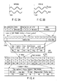
- FIG. 1 is a diagram illustrating an example in which recording tracks are subjected to a wobble modulation in order to address an optical disk recording medium.
- FIG. 1 shows the relationship among signals during the wobble modulation. Digital data is reproduced from (or recorded in) the meandering recording tracks. On this occasion, the recorded data are recorded at specified positions. Physical address information determining the specified positions is obtained by reading and demodulating the wobble signals from the recording tracks.
- FIG. 1 shows the relationship between a read beam L-beam on a track WB-track, a detected wobble signal WB-signal, and a high frequency signal RF-signal for read digital data.
- FIG. 2 is a chart showing the layout of physical address information for a structure in which both lands and grooves of each recording track in an optical disc recording medium are used.
- a zone system An optical disk recording medium is divided into a plurality of zones in a radial direction. In each zone, the recording capacity constitutes a specified segment packet. A "zone number”, a “track number”, and a “segment number”, which are physical address information, are embedded in each zone by subjecting the groove tracks to the wobble modulation. When one zone changes to another zone, a division angle (the division angle of the periphery of the disk as viewed from its center) with which the segments within the zone are formed is changed so that the segments have a substantially equal recording density.
- the optical disk is divided into a number of zones Z0, Z1, ⁇ .
- the recording tracks within the same zone has physical segments aligned with one another in the radial direction.
- FIG. 2 shows an example of arrangement of physical segments in the vicinity of a zone boundary (between a zone m and a zone m+1).
- a lead-in area, data area, and lead-out area of an optical disk are each composed of a zone, a plurality of tracks, and a plurality of physical segments.
- L denotes a land
- G denotes a groove.
- a physical segment is identified by a zone number, a track number, and a segment number.
- Each zone contains segments with the same physical segment number.
- the angular distance between the first channel bits of physical segments in adjacent tracks is preferably shorter than ⁇ 4 channel bits.
- the angular distance is a spread angle observed when the radially outer periphery of the disk is viewed from its center.
- the physical segment number at the start position of a track is zero and is located at the boundary between zones.
- the angular distance between the first channel bits of physical segments at two track start positions is at most ⁇ 256 channel bits.
- the address of a land track adjacent to a zone boundary cannot be read.
- FIGS. 3A and 3B are diagrams showing a modulation rule used if information is embedded by the wobble modulation.
- a sine wave or non-modulated wave (NPW) of a wobble signal is utilized as the bit information "0”.
- An inverted wave or modulated wave (IPW) of the wobble signal is utilized as the bit information "1”.
- This linkage rule is also used to configure synchronizing signals.
- FIG. 4 is a diagram of the entire data structure of physical addresses, showing the relationship among the physical addresses. Before describing physical addresses, description will be given of various terms.
- Wobbles are formed by meandering grooves.
- a wobble modulated portion is obtained by changing the phase of wobbles in accordance with data and has a meaning as data. In this case, one bit of data is expressed by 4 wobbles (4 cycles).
- a WDU (Wobble Data Unit) is a unit used to express information by the wobble modulation and is referred to as a transmission unit herein.
- the total number of wobbles in the WDU is 84.
- the WPA is composed of a synchronizing section (SYNC), an address field, and a unity field.
- the synchronizing section (SYNC) is composed of one WDU.
- the address field contains 13 WDUs.
- the unity field is composed of three WDUs.
- the WDUs constituting the synchronizing section have a fixed form in which an IPW of 6 wobbles, an NPW of 4 wobbles, an IPW of 6 wobbles, and an NPW of 68 wobbles are arranged in this order.
- a WDU in the address field is composed of an IPW of 4 wobbles, "b2" of 2 wobbles, "b1" of 4 wobbles, "b0” of 4 wobbles, and an NPW of 68 wobbles arranged in this order. Accordingly, a WDU in the address field contains 3 bits of information (b2, b1, and b0) as variable contents.
- the unity field is composed only of an NPW of 84 wobbles.
- the IPW placed at the leading end of the WDU is a wobble data unit synchronizing signal.
- the WPAs are connected together to form track wobbles. Accordingly, a period determined by the unit of WPAs (the unit of transmission blocks) is equal to a period with which physical address data is embedded. Moreover, at least 4 wobbles at the leading end of each WDU having data are configured as an IPW (wobble data unit synchronizing signal). This facilitates the identification of the leading end of the WDU. As a result, in each WDU, 68 wobbles following the embedded address information are defined as an NPW. As described above, in the WPA, the whole physical address data is composed of 39 bits. Therefore, the address field requires 13 WDUs. A block synchronizing signal is placed in the leading WDU of the WPA. The trailing three units constitute a non-modulated unit (unity field).
- a plurality.of transmission blocks are defined each of which is formed of a plurality of transmission units (WDUs) each containing a data modulated wave.
- the transmission unit (WDU) contains a carrier of N cycles. In a unit leading part, the carrier is a fixed modulated wave, in a unit trailing part, the carrier is a non-modulated wave, and between the unit leading part and the unit trailing part, the carrier is a data modulated wave.
- the transmission block (WPA) contains M transmission units. The transmission unit at the leading end of the transmission block is defined as a synchronizing section. A predetermined number of transmission units in the trailing part of the block are all defined as a unity field containing a non-modulated wave. The plurality of transmission units between the block trailing part and the block leading end are defined as an address field containing a data modulated wave.
- information containing video data, management data, or the like is recorded in recording tracks such as groove or land tracks, described above.
- the recorded data is composed of 77,376 bytes of data, leading 71 bytes of VFO (a fixed frequency signal that facilitates the generation of a data modulation channel clock during a reproducing operation), followed by a "post amble (PA) field” used to connect data blocks together, a "reserved field”, and a “buffer field”; the trailing three fields are composed of 22 bytes in total.
- a total of 77,469 bytes are recorded in 7 physical segments (9,996 wobbles).
- the user data is recorded in the area specified by the address data in the physical segments.
- the reading of the address data from the physical segments is important.
- synchronizing signals are detected from wobble signals to synchronize a period counter for WPAs (transmission blocks) with the transmission block.
- An output from the period counter is utilized to generate timing signals.
- the timing signals are then used to extract sample signals from the wobble signals.
- the sample signals are then demodulated to obtain address information.
- FIG. 5 is a diagram showing an example of the configuration of a timing control circuit using a method of synchronizing the period counter.
- a wobble signal WB-signal read from the recording medium is sent to a wobble phase synchronizing circuit R1 that generates a clock used to read and demodulate address data.
- the wobble phase synchronizing circuit R1 generates an output clock WB-CK.
- This clock actually gradually increases the frequency of the wobble signal so that the frequency increased clock signal becomes the channel bit clock frequency of a data recording signal for data recording.
- the clock divides the frequency of the signal again. That is, the clock is used for the wobble frequency or to read address data.
- the output clock WB-CK from the wobble phase synchronizing circuit R1 is assumed to be a clock for the wobble frequency.
- the wobble signal WB-signal is further sent to a phase detector R2 that distinguishes an NPW from an IPW.
- the output clock from the wobble phase synchronizing circuit R1 is utilized to determine whether the wobble signal WB-signal is an NPW or an IPW.
- a signal for a result of phase determination from the phase detector R2 is sent to a synchronizing signal detector R3 and a demodulator R8.
- the synchronizing signal detector R3 detects the synchronizing signal (SYNC), described in FIG. 4.
- the demodulator R8 demodulates bit data.
- the output clock WB-CK, from the wobble phase synchronizing circuit R1 is sent to a frequency divider R4 that divides a frequency into 84 pieces.
- a frequency division output from the frequency divider R4 is inputted to a frequency divider R5 that divides each frequency into 17 pieces.
- the frequency dividers R4 and R5 constitute a period counter circuit.
- the period counter circuit is initialized (synchronized) by synchronizing with a WPA synchronization detection signal PB-SYNC detected by the synchronizing signal detector R3.
- the WPA synchronization detection signal PB-SYNC can be considered to be a result of detection of a false synchronizing signal (NSYNC).
- the WPA synchronization detection signal PB-SYNC performs an initializing operation, without directly synchronizing the periodic counter circuit, only when the WPA synchronization detection signal PB-SYNC is detected within a gate pulse WG from a window gate circuit R6 utilizing an output from the period counter circuit.
- the period counter circuit is permanently not synchronized.
- a false synchronizing signal detector R7 checks the number of times the WPA synchronization detection signal PB-SYNC has consecutively failed to be detected within the gate pulse WG. If the WPA synchronization detection signal PB-SYNC has failed to be detected within the gate pulse WG a specified number of times, an AND circuit A1 is controlled via an OR circuit 01 to establish an open state. This allows the WPA synchronization detection signal PB-SYNC from the signal detecting circuit R3 to be outputted through the AND circuit A1. Consequently, the frequency dividers R4 and R5 are forcedly initialized for synchronization.
- the false synchronizing signal NSYNC is excluded on the basis of a time correlation characteristic using the periodicity of the WPA synchronization detection signal PB-SYNC.
- the period counter circuit composed of the thus synchronized frequency dividers R4 and R5, creates a timing control signal.
- the demodulator R8 and a data setting section R9 read the data "segment information", “segment address”, “zone address”, “parity address”, "groove address”, and "land address”, shown in FIG. 4.
- FIG. 6 is a flow chart schematically showing operations of the circuit in FIG. 5.
- the synchronizing signal is detected on the basis of its synchronizing pattern (step ST1). It is detected whether or not the synchronizing signal is within the gate pulse WG (step ST2). If the synchronizing signal is within the gate pulse WG, the frequency dividers R4 and R5 are initialized. Further, the false synchronizing signal detector R7 is reset (step ST4). If the synchronizing signal is out of the gate pulse WG, it is determined whether or not a count in the false synchronizing signal detector R7 has a set value (step ST3). If the count does not have the set value, it is incremented by one (step ST5). The procedure then shifts to a process of detecting the next synchronizing pattern. If the count has the set value, the procedure shifts to the process of forcedly initializing the frequency dividers R4 and R5 as previously described.
- the period counter synchronizing system shown in FIG. 5 excludes the false synchronizing signal using the period of arrangement of the physical addresses, that is, the time correlation characteristic of arrival period of the WPA shown in the example in FIG. 4.
- the false synchronizing signal NSYNC is generated at the same period, malfunction disadvantageously cannot be prevented.
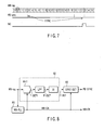
- FIG. 7 shows an example of such a problem.
- FIG. 7 shows an example in which there is a defect in the correct synchronizing signal SYNC area when the physical addresses are reproduced under the condition of the consecutive transmission of WPAs.
- FIG. 7 shows a wobble signal (WB-signal), a synchronization detection signal PB-SYNC (in this case, a false synchronizing signal NSYNC), and a window gate pulse (WG).
- WB-signal wobble signal
- PB-SYNC synchronization detection signal
- WG window gate pulse
- the period counter synchronizes with the next false synchronizing signal NSYNC.
- the window gate pulse WG is generated. Then, a similar false synchronizing signal NSYNC is detected. Malfunction continues until this phenomenon is eliminated.
- the false synchronizing signal NSYNC is likely to be generated even in the address data area owing to a decrease in S/N ratio.
- the synchronizing signal is a combination of an IPW (6WB), an NPW (4WB), and an IPW (6WB), and the address data uses a 4WB unit. It is thus unlikely to form a synchronizing signal pattern. However, erroneous detections are more likely to occur as described later in FIGS. 8, 9 and 10.
- FIG. 8 shows a part composed of the phase detector R2 and synchronizing signal detector R3.
- FIG. 9 shows the waveforms of signals from the components.
- a wobble signal is modulated using physical address data.
- a multiplier MX1 multiplies the modulated wobble signal by the output clock WB-CK, generated by the wobble phase synchronizing circuit R1.
- the multiplier MX1 provides a multiplication output signal P-DET1 as shown in FIG. 9.
- the signal P-DET1 is passed through a low pass filter LPF to generate an output signal P-DET2.
- a slicer Sli then slices the signal P-DET2 to output a binarized signal P-DET having a binary value.
- the length of "0” or “1” in the binarized signal P-DET is detected using the clock WB-CK.
- the WPA synchronization detection signal PB-SYNC, the data "0”, or the data "1” is selectively demodulated.
- FIG. 10 is a timing chart showing an example in which the S/N ratio of the wobble signal WB-signal decreases due to the crosstalk signal between adjacent tracks, a defect, or the like.
- the boundary between an NPW and an IPW cannot be reliably detected.
- an inverted part of the binarized signal P-DET may take an unstable position. If the synchronizing signal is detected in such a situation, then in the address area, it is more likely to determine an IPW (4WB), an NPW (4WB), and an IPW (4WB) to be an IPW (6WB), an NPW (4WB), and an IPW (6WB) after binarization.
- the present invention makes further improvements. Specifically, a reliable synchronizing method and apparatus is provided by using the nature of the physical address structure shown in FIG. 4 as a referential example.
- FIG. 11 is a diagram showing the configuration of a read timing control device according to a first improved example.
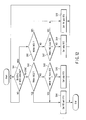
- FIG. 12 is a flow chart showing an example of operations of the read timing control device.
- the wobble signal WB-signal read from the recording medium is sent to the wobble phase synchronizing circuit R1, which generates a clock.
- the wobble phase synchronizing circuit R1 generates the output clock WB-CK.
- This clock actually gradually increases the frequency of the wobble signal so that the signal has the channel bit clock frequency of a data recording signal for data recording.
- the clock divides the frequency of the signal again. That is, the clock is used for the wobble frequency or to read address data.
- the output clock WB-CK from the wobble phase synchronizing circuit R1 is assumed to be used for the wobble frequency.
- the wobble signal WB-signal is further sent to the phase detector R2 that distinguishes an NPW from an IPW.
- the output clock from the wobble phase synchronizing circuit R1 is utilized to determine whether the wobble signal WB-signal is an NPW or an IPW.
- a signal for a result of phase determination from the phase detector R2 is sent to the synchronizing signal detector R3 and the demodulator R8.
- the signal for the result of the phase determination is further sent to a wobble data unit (WDU) detector R10.
- the wobble data unit (WDU) detector R10 detects the arrival of the wobble data unit (step SA1).
- the wobble data unit synchronizing signal PB-WDU is inputted to a counter R72 and the AND circuit A1.
- the counter R72 is used as a sub-period counter of the 1/84 frequency divider R4.
- the counter R72 periodically outputs a gate signal.
- a 1/84 frequency divider R4 is reset if the wobble data unit synchronizing signal PB-WDU is obtained at the same time within a wobble data unit (WDU) window gate pulse WG1.
- the 1/84 frequency divider R4 is reset even if the wobble data unit synchronizing signal PB-WDU is present within the window gate pulse WG1a outputted by the counter R72 (steps SA2, SA3, and SA4).
- the signal PB-WDU is not present within the pulse WG1 or is not present within the window gate pulse WG1a outputted by the counter R72, only the counter R72 is forcedly reset. That is, only the counter R72 is reset and the process waits for the next detection result (step SA9).
- operations may be performed as shown in the example in FIG. 5. Specifically, if the signal PB-WDU is out of the period of the pulse WG1, the counter R72 continues counting. Once the count in the counter R72 reaches a predetermined value, the AND circuit A1 is controlled via an OR circuit O1 to forcedly initialize the 1/84 frequency divider R4 using the timing set by the signal PB-WDU.
- the window gate pulse WG1 is created by a window gate circuit R61 using an output from the 1/84 frequency divider R4.
- the frequency division output from the 1/84 frequency divider R4 is further inputted to a 1/27 frequency divider R5, thus constituting a period counter circuit.
- the synchronizing signal detector R3 detects the synchronizing signal section (SYNC), described in FIG. 4, and outputs the WPA synchronization detection signal PB-SYNC (step SA1).
- the WPA synchronization detection signal PB-SYNC is inputted to the counter R72 and an AND circuit A2.
- a counter R73 is reset when the WPA synchronization detection signal PB-SYNC and a window gate pulse WG2 are obtained at the same time (steps SA6, SA7, and SA8).
- the signal PB-SYNC does not synchronize with the pulse WG2, counting continues.
- the AND circuit A2 is controlled via an OR circuit 02 to forcedly initialize the 1/17 frequency divider R5 using the timing set by the signal PB-WDU (step SA9).
- the window gate pulse WG2 is created by the window gate circuit R62 using an output from the 1/17 frequency divider R5.
- This embodiment utilizes a pattern in which the WDU (transmission unit) shown in FIG. 4 is configured so that at least only the first 16 wobbles are modulated so as to have certain contents, while the remaining wobbles have an NPW phase, with the first 4 wobbles defined as an IPW.
- a wobble data unit detector R10 detects a WDU division point.
- the 1/84 frequency divider R4 is initialized.
- the synchronizing signal detector R3 initializes only the 1/17 frequency divider R5. That is, the 1/84 frequency divider R4 is initialized for WDU synchronization, while the 1/17 frequency divider R5 is initialized for segment synchronization.
- the wobble data unit detector R10 generates a large number of detection results. Consequently, it is unlikely to make the detection of the period of the whole WPA unreliable.
- the method of initializing the 1/84 frequency divider R4 comprises correcting a detected phase difference on the basis of the initialize timing and the contents of the counter of the 1/84 frequency divider R4 rather than forcedly presetting a general specified value. This prevents significantly erroneous settings even if the timing for the detection results accompanies jitter. Therefore, the system becomes more reliable.
- the unit detection signal PB-WDU or the block synchronization detection signal PB-SYNC is not present within from the period of the window gate signal WG1 or WG2, respectively, generated by the output from the N or M period counter R4 or R5, respectively, provided that the signal PB-WDU or PB-SYNC is found within the window gate signal WG1a or WG2a, respectively, the corresponding N or M period counter R4 or R5 is initialized.
- the unit detection signal PB-WDU or the block synchronization detection signal PB-SYNC is not present within any periods of the window gate signals WG1, WG2, WG1a, and WG2a, only the corresponding sub-period counter R72 or R73 is initialized. The process then waits for the next detection result.
- FIG. 13 shows another embodiment.
- a unity field (UF) detector R11 is added to the configuration shown in FIG. 11.
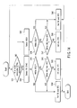
- FIG. 14 is a flow chart showing an example of operations of this embodiment.
- This embodiment focuses on the fact that in the WPA composed of the plurality of wobble data units WDU, shown in the example in FIG. 4, the last WDU is not modulated and is used as a unity field.
- Another focus is on the presence of the WPA synchronization detection signal PB-SYNC during a specific period after the detection of an NPW the amount of which exceeds the amount of wobbles in one WDU.
- a gate signal UF-G is generated for a specific period. Then, only during that period, the synchronizing signal detector R3 is operated, or the detection result PB-SYNC is outputted only during the generation of the gate signal UF-G even though the synchronizing signal detector R3 is operated (step SB1 and SB2).
- the other operations are the same as those in the above embodiment. Accordingly, the parts of the flow chart in FIG. 14 which correspond to the flow chart in FIG. 12 are denoted by the same reference numerals as those in FIG. 12.
- This configuration accepts the WPA synchronization detection signal PB-SYNC only when the gate signal UF-G is obtained. It is thus possible to prevent the false synchronizing signal from causing initialization. Specifically, it is impossible that the false synchronization shown in FIG. 7 occurs. This makes the system much more reliable.
- the other parts are the same as those of the circuit shown in FIG. 11. Accordingly, their description is omitted.
- FIG. 15 shows the relationship among the wobble signal WB-signal, the synchronizing signal SYNC, the unity field detection signal UF-G, and the gate signal WG2 during the operation of the above circuit.
- the method of initializing the frequency divider R4 may comprise correcting the phase of the counter, the frequency divider R4, by increasing or reducing the number of clocks WB-CK in accordance with the initialize timing and a phase difference based on the contents of the counter, rather than forcedly presetting a general specified value.
- FIG. 16 shows a clock correcting operation performed in the frequency divider R4.
- an initialize signal (Initialize-G) is generated
- the clock WB-CK is corrected so as to increment or decrement by one, on the basis of the contents of the counter of the frequency divider R4.
- the figure shows the waveform (-WB-CK) of the decremented clock and the waveform (+WB-CK) of the incremented clock.
- FIG. 17 shows another embodiment.
- FIG. 18 is a flow chart showing an example of operations of this embodiment.
- This embodiment has a function by which the unity field detector R11 is controlled to restrict the synchronizing signal detector R3. It thus initializes the 1/84 frequency divider R4 and 1/27 frequency divider R5, constituting the period counter circuit, using only the WPA synchronization detection signal PB-SYNC (having passed through the AND circuit A1). This configuration can also adequately prevent the false synchronizing signal from causing initialization.
- FIG. 19 is a diagram showing an approach to improving the reliability of detection of a WDU division point.
- the WDU detector R10 shown in FIGS. 11 and 13, utilizes the characteristics of the data structure of WDUs in the address field, shown in FIG. 4. Specifically, the WDU division point is detected by detecting that the preceding NPW (68 wobbles) continues for a specific period to detect the first IPW of the WDU to be detected. However, the leading IPW may be erroneously determined owing to a defect or the like. Accordingly, the detection of the WDU division point is made more reliable by utilizing the nature that if the data succeeding the leading IPW has its phase inverted, it is positioned at a distance equal to 4 wobbles.
- FIG. 1 the WDU division point is detected by detecting that the preceding NPW (68 wobbles) continues for a specific period to detect the first IPW of the WDU to be detected.
- the leading IPW may be erroneously determined owing to a defect or the
- FIG. 19 illustrates the types of waveforms assumed as the configuration of WDUs in the address field, as (Type-a) to (Type-h).
- the figure also shows phase inversion point patterns corresponding to the respective types. Detecting the phase inversion point enables the WDU division point to be much more reliably detected.
- the frequency divider R4 is initialized near the 20-th wobble because the detection result appears after 16 wobbles have been obtained.
- the initialize point is not within the data area, thus advantageously hindering variations attributed to the initialization.
- the transmission units constituting the transmission block include a transmission block synchronizing signal (first WDU) and distributed control data (the data in the address field).
- the synchronizing signal and control data are embedded by subjecting the waveforms of the wobbles to the data modulation.
- main period counter means is constructed by connecting an N period counter (1/84 frequency divider) and an M period counter (1/17 frequency divider) together.
- Transmission block synchronization detecting means (synchronization signal detector R3) detects a synchronizing signal from the transmission unit (first WDU) located at the leading end of the transmission block modulated by the block synchronizing signal. The transmission block synchronization detecting means then outputs a block synchronization detection signal (PB-SYNC).
- initialize means (O1, A1, 02, and A2) initializes the N period counter (1/84 frequency divider) to a set value using the unit detection signal (PB-WDU), detected by the transmission unit detecting means (WDU detector R10).
- the initialize means (O1, A1, 02, and A2) also initializes the M period counter (1/17 frequency divider) to a set value using the block synchronization detection signal (PB-SYNC), detected by the transmission block synchronization detecting means (synchronizing signal detector R3).
- means for generating timing signals used by the main period counter means composed of the N period counter and the M period counter, to read modulated data contained in the transmission units.
- the present invention is effective in fields in which, for example, a carrier is used to generate a system clock for a system that transmits main information and for a system that records main information.
- control data or the like is embedded in the carrier (the carrier is modulated)
- the embedded modulated area constitutes a part of the carrier.
- the data is distributively embedded in the carrier.
- the separate counters are used to provide a period for the transmission units and for the transmission blocks. Period synchronization is separately executed on these counters. This prevents the apparatus from being falsely synchronized.
- a transmission unit division point is detected by detecting the non-modulated area of the preceding transmission unit and then the modulated area of the next transmission unit. The introduction of this system enables the transmission unit division point to be stably detected.
- the transmission unit detecting means detects the transmission unit division point by detecting the non-modulated area in the latter half of the transmission unit and the modulated area in the modulated leading part of the next transmission unit.
- the transmission unit detecting means thus obtains a unit detection signal.
- the block synchronization detecting means detects transmission units none of which are modulated (unity field: FIGS. 13 and 17), to detect the block synchronization detection signal from the next transmission unit. Then, the block synchronization detecting means considers this block synchronization detection signal to be valid.
- the unit detection signal detected by the transmission unit detecting means is used to initialize the N period counter to a set value.
- the block synchronization detection signal detected by the transmission block synchronization detecting means is used to initialize the M period counter to a set value. In this case, the initialization is carried out only when the unit detection signal and the block synchronization detection signal are detected within window gate signals generated by outputs from the N and M period counters, respectively.
- Another aspect of the present invention further has a first sub-period counter (R72) corresponding to the N period counter and a second sub-period counter (R73) corresponding to the M period counter.
- R72 first sub-period counter
- R73 second sub-period counter
- the sub-period counters are installed so that if a detection result is generated at a distance within one period, the corresponding period counter is synchronized. Since non-consecutive detection signals are likely to be false, this aspect can deal with the correct synchronization at any time while preventing erroneous synchronizations.
- Another aspect of the present invention further has a first sub-counter corresponding to the N period counter and a second sub-counter corresponding to the M period counter. Even if the unit detection signal or the block synchronization detection signal is not present within the window gate signal generated by the output from the N or M period counter, respectively, the count in the corresponding sub-counter is controlled. Then, once the count reaches a predetermined value, the N or M period counter is forcedly initialized. This is also within the scope of the present invention.
- This configuration is characterized in that the period counter is composed of the N period counter and M period counter, which are connected together, and in that the N and M period counters separately execute initialization.
- the initialize means initializes the N and M period counters, predetermined values are set in these counters.
- the initialize means initializes the N and M period counters
- the N and M period counters are not preset to predetermined values, and the count in the N period counter is controlled to be closer to a predetermined value as follows. If the count in the N period counter at a point in time for initialization is larger than the predetermined value, a counter input clock is decremented by one clock. On the other hand, if the count is smaller than the predetermined value, the input clock is incremented by one clock for supply. This is also within the scope of the present invention.
- the N period counter synchronizes the transmission units constituting the whole block. Accordingly, the timing for detection of a transmission unit may vary depending on the grade of the signal.
- the carrier is composed of wobble signals from recording tracks in a recording medium.
- the control data is composed of physical address information.
- a configuration used to generate timing clocks for data recording signals on the basis of wobbling recording tracks in a recording medium such as an optical disk if physical addresses are provided by wobble modulation, timings for reading the physical addresses are controlled by using a counter for an address recording arrangement period. In this case, the capability of synchronizing the period counter is important.
- the level of modulation cannot be significantly increased if the physical addresses are subjected to a track wobble modulation. As a result, a high S/N ratio cannot be obtained. Consequently, for timings for detecting the synchronizing signal, the detection may often be erroneous and the detecting timing may often vary.
- the above configuration enables reliable synchronizations even with such a defect.
- the present invention can be employed not only to reproduce information from a recording medium but also for a transmission system that receives signals for the above transmission units and transmission blocks each composed of the transmission units.
- the present invention is not limited to the above embodiments.
- the components of the embodiments may be varied without departing from the spirit of the invention.
- various inventions can be formed by properly combining a plurality of the components disclosed in the above embodiments. For example, some of all the components shown in the embodiments may be omitted.
- components of the different embodiments may be properly combined together.
Landscapes
- Signal Processing For Digital Recording And Reproducing (AREA)
- Optical Recording Or Reproduction (AREA)
- Synchronisation In Digital Transmission Systems (AREA)
Abstract
A WDU is defined as a unit composed of a carrier
of N cycles which carrier contains data depending on
whether or not modulation is executed. A WPA is
defined as a unit composed of a set of M of the WDUs.
When the WPAs are consecutively inputted, each WDU and
each WPA are detected. Further, an N period counter
(R4) and an M period counter (R5) are used to obtain
timing control signals for sampling the data. Then,
WDU detecting means (R10) obtains a WDU synchronization
detection signal PB-WDU indicative of a division point
between the WDUs. WPA detecting means obtains a WPA
synchronization detection signal PB-SYNC. The WDU
synchronization detection signal is used to initialize
the N period counter (R4) to a set value. The WPA
synchronization detection signal is used to initialize
the M period counter (R5) to a set value.
Description
The preset invention relates to a synchronizing
method and apparatus that is effective in obtaining
synchronizing signals for signals detected from, for
example, an optical disk.
Information recording and reproducing systems
using an optical disk as a recording medium have been
popularized through the spread of CD-R disk- and CD-RW
disk-based systems. Further, in recent years, for
example, DVD-R, DVD-RW, and DVD-RAM media, based on the
DVD system, have been commercialized. With an increase
in their storage capacities, these media have been
rapidly diffused. The popularization of video
recorders using a DVD recording medium are assumed to
be a result of the recognition of their functions
meeting users' demands; such as easier editing,
faster retrieval, and improved image quality based
on digitalization.
If digital information is recorded in a recording
medium, a recording apparatus first reads physical
addresses embedded in a recording track. The recording
apparatus then sequentially records packetized
recording information at recording positions in
accordance with a certain rule while referencing
the physical addresses.
A system that embeds physical addresses in
a recording medium embeds address data or the like
by subjecting recording tracks to wobble modulation.
This embedding system embeds address data in recording
tracks using a particular period. Accordingly, the
apparatus requires an internal period counter to
acquire the address data, understand its contents,
and control read positions. It is also necessary to
synchronize the operation of the period counter with
a particular position of the address data.
To achieve this period synchronization,
synchronizing signals are embedded in the recording
tracks at a particular period together with the address
data and the like. Even if the period counter is
synchronized with the address data on the basis of the
synchronizing signals, the wobble modulation method or
the like may undergo the crosstalk between adjacent
tracks, various defects, variations in characteristics
among recording media, or the like. Consequently, data
read timings have often been erroneous. Thus, a method
of synchronizing the period counter is important
because it determines the capability of reading address
data or the like, which is essential information for
determining recording positions.
In general, a method of controlling timings
for data streams with a period characteristic and
synchronizing the data streams comprises generating
timing control signals using the period counter as
a main component. In this case, the period counter is
synchronized (initialized to a particular value) using
a reproduction synchronizing signal detected from an
input signal. However, a false synchronizing signal
may be detected as the reproduction synchronizing
signal, resulting in erroneous timing control. In view
of such a problem, a system has been introduced which
synchronizes the period counter using a function to
determine whether or not a detected reproduction
synchronizing signal is real.
[Patent Document 1] Jpn. Pat. Appln. KOKAI
Publication No. 2000-163766
However, the conventional synchronizing
apparatuses and methods are insufficiently reliable and
are desired to be further improved. In particular,
there is a demand for the improvement of accuracy of
apparatuses used to detect physical addresses in
a recording medium. This is due to the increased
density of recording media, leading to the increased
possibility of reproducing a false synchronizing
signal. For example, if the recording medium has
a defect at a regular synchronizing signal position and
a false synchronizing signal is generated at an offset
position, permanent synchronization with the false
synchronizing signal may occur.
It is thus an object of the present invention to
provide a synchronizing method and apparatus which
enables a period counter to be reliably synchronized
with read information.
According to embodiments of the present invention
provides an apparatus which reproduces control
data, wherein a carrier of N cycles is composed of
transmission units, a transmission block is composed of
M sets of transmission units, some of the particular
transmission units constituting the transmission block
are composed of a block synchronizing signal and
a section containing modulated distributed control
data, and if transmission blocks are consecutively
transmitted, the apparatus comprising:
This summary of the invention does not necessarily
describe all necessary features so that the invention
may also be a sub-combination of these described
features.
The invention can be more fully understood from
the following detailed description when taken in
conjunction with the accompanying drawings, in which:
Embodiments of the present invention will be
described below with reference to the drawings.
Before describing specific examples of the present
invention, description will be given of a technique
that is essential to the present invention. An optical
disk normally has spirally formed recording tracks.
Each of the recording tracks is divided into physical
segments each having a predetermined length. Each of
the physical segments is provided with an address.
The address is written in the corresponding physical
segment as preformat data.
An optical disk employing a CLV system having a
constant recording line density uses a uniform physical
segment length. An excessively long physical segment
increases the time required to search for address
information during a random access. Accordingly, the
physical segment length is selected so that one round
corresponds to 10 to several dozen physical segments.
A preformatting method comprises forming wobble
signals in data recording tracks which signals are
based on meandering of grooves, and using the wobble
signals to express format information. If format
information is recorded using wobble signals, the
signals are subjected to a modulation such as a phase
inversion or a frequency change.
FIG. 1 is a diagram illustrating an example in
which recording tracks are subjected to a wobble
modulation in order to address an optical disk
recording medium. FIG. 1 shows the relationship among
signals during the wobble modulation. Digital data
is reproduced from (or recorded in) the meandering
recording tracks. On this occasion, the recorded data
are recorded at specified positions. Physical address
information determining the specified positions is
obtained by reading and demodulating the wobble signals
from the recording tracks.
FIG. 1 shows the relationship between a read beam
L-beam on a track WB-track, a detected wobble signal
WB-signal, and a high frequency signal RF-signal for
read digital data.
FIG. 2 is a chart showing the layout of physical
address information for a structure in which both lands
and grooves of each recording track in an optical disc
recording medium are used.
Addressing based on the wobble modulation is
executed on groove tracks. However, if information is
recorded in or reproduced from land tracks, the correct
addressing must be established. Thus, an addressing
structure called a zone system is employed. An optical
disk recording medium is divided into a plurality of
zones in a radial direction. In each zone, the
recording capacity constitutes a specified segment
packet. A "zone number", a "track number", and
a "segment number", which are physical address
information, are embedded in each zone by subjecting
the groove tracks to the wobble modulation. When one
zone changes to another zone, a division angle (the
division angle of the periphery of the disk as viewed
from its center) with which the segments within the
zone are formed is changed so that the segments have
a substantially equal recording density. The recording
capacity is thus optimized. With the configuration
shown in FIG. 2, even with the land/groove system,
address information in groove wobble signals from
adjacent tracks has the same values except for the
track number Physical address information can also be
read from the land tracks. By arranging track numbers
for the lands and for the grooves, it is possible
to obtain information from both lands and grooves.
Consequently, no problems occur.
The optical disk is divided into a number of zones
Z0, Z1, ···. The recording tracks within the same zone
has physical segments aligned with one another in the
radial direction.
FIG. 2 shows an example of arrangement of physical
segments in the vicinity of a zone boundary (between
a zone m and a zone m+1). In this example, a lead-in
area, data area, and lead-out area of an optical disk
are each composed of a zone, a plurality of tracks, and
a plurality of physical segments. "L" denotes a land,
and "G" denotes a groove. A physical segment is
identified by a zone number, a track number, and
a segment number. Each zone contains segments with
the same physical segment number. In each zone, the
angular distance between the first channel bits of
physical segments in adjacent tracks is preferably
shorter than ±4 channel bits. The angular distance
is a spread angle observed when the radially outer
periphery of the disk is viewed from its center.
The physical segment number at the start position of
a track is zero and is located at the boundary between
zones. In each lead-in area, each data area, and each
lead-out area, the angular distance between the first
channel bits of physical segments at two track start
positions is at most ±256 channel bits. The address
of a land track adjacent to a zone boundary cannot be
read.
FIGS. 3A and 3B are diagrams showing a modulation
rule used if information is embedded by the wobble
modulation. A sine wave or non-modulated wave (NPW) of
a wobble signal is utilized as the bit information "0".
An inverted wave or modulated wave (IPW) of the wobble
signal is utilized as the bit information "1". This
linkage rule is also used to configure synchronizing
signals.
FIG. 4 is a diagram of the entire data structure
of physical addresses, showing the relationship among
the physical addresses. Before describing physical
addresses, description will be given of various terms.
Wobbles are formed by meandering grooves.
A wobble modulated portion is obtained by changing
the phase of wobbles in accordance with data and has
a meaning as data. In this case, one bit of data is
expressed by 4 wobbles (4 cycles).
A WDU (Wobble Data Unit) is a unit used to express
information by the wobble modulation and is referred to
as a transmission unit herein. The total number of
wobbles in the WDU is 84. A WPA (Wobble Address in
Periodic position) is a unit composed of a set of
M (=17) WDUs and is referred to as, for example,
a transmission block herein. The WPA is composed of
a synchronizing section (SYNC), an address field, and
a unity field. The synchronizing section (SYNC) is
composed of one WDU. The address field contains 13
WDUs. The unity field is composed of three WDUs.
The WDUs constituting the synchronizing section
(SYNC) have a fixed form in which an IPW of 6 wobbles,
an NPW of 4 wobbles, an IPW of 6 wobbles, and an NPW of
68 wobbles are arranged in this order. A WDU in the
address field is composed of an IPW of 4 wobbles, "b2"
of 2 wobbles, "b1" of 4 wobbles, "b0" of 4 wobbles,
and an NPW of 68 wobbles arranged in this order.
Accordingly, a WDU in the address field contains 3 bits
of information (b2, b1, and b0) as variable contents.
The unity field is composed only of an NPW of 84
wobbles. The IPW placed at the leading end of the WDU
is a wobble data unit synchronizing signal.
Physical address data indicating the position of
a physical segment is composed of 39 bits including
"3 bits of segment information", "6 bits of segment
address", "5 bits of zone address", "1 bit of parity
address", "12 bits of groove address", and "12 bits of
land address". These 39 bits are divided into groups
of 3 bits each. The groups of bits are distributed
among the WDUs, in which the bits are embedded by
a modulating process. Therefore, the bits are
distributed among the 13 WDUs constituting the address
field (3 × 13 = 39).
The WPAs are connected together to form track
wobbles. Accordingly, a period determined by the unit
of WPAs (the unit of transmission blocks) is equal to
a period with which physical address data is embedded.
Moreover, at least 4 wobbles at the leading end of each
WDU having data are configured as an IPW (wobble data
unit synchronizing signal). This facilitates the
identification of the leading end of the WDU. As a
result, in each WDU, 68 wobbles following the
embedded address information are defined as an NPW.
As described above, in the WPA, the whole physical
address data is composed of 39 bits. Therefore, the
address field requires 13 WDUs. A block synchronizing
signal is placed in the leading WDU of the WPA.
The trailing three units constitute a non-modulated
unit (unity field).
That is, a plurality.of transmission blocks (WPAs)
are defined each of which is formed of a plurality of
transmission units (WDUs) each containing a data
modulated wave.
The transmission unit (WDU) contains a carrier
of N cycles. In a unit leading part, the carrier is
a fixed modulated wave, in a unit trailing part, the
carrier is a non-modulated wave, and between the unit
leading part and the unit trailing part, the carrier is
a data modulated wave. The transmission block (WPA)
contains M transmission units. The transmission unit
at the leading end of the transmission block is defined
as a synchronizing section. A predetermined number of
transmission units in the trailing part of the block
are all defined as a unity field containing a non-modulated
wave. The plurality of transmission units
between the block trailing part and the block leading
end are defined as an address field containing a data
modulated wave.
Then, information containing video data,
management data, or the like is recorded in recording
tracks such as groove or land tracks, described above.
In this case, the recorded data is composed of
77,376 bytes of data, leading 71 bytes of VFO (a fixed
frequency signal that facilitates the generation of
a data modulation channel clock during a reproducing
operation), followed by a "post amble (PA) field" used
to connect data blocks together, a "reserved field",
and a "buffer field"; the trailing three fields are
composed of 22 bytes in total. A total of 77,469 bytes
are recorded in 7 physical segments (9,996 wobbles).
In accordance with the above rule, the user data
is recorded in the area specified by the address data
in the physical segments. Thus, the reading of the
address data from the physical segments is important.
If the physical addresses configured as described
above are read from the recording medium in which the
physical addresses are recorded, synchronizing signals
are detected from wobble signals to synchronize a
period counter for WPAs (transmission blocks) with the
transmission block. An output from the period counter
is utilized to generate timing signals. The timing
signals are then used to extract sample signals from
the wobble signals. The sample signals are then
demodulated to obtain address information.
FIG. 5 is a diagram showing an example of the
configuration of a timing control circuit using a
method of synchronizing the period counter. First,
operations of this circuit will be described in brief.
A wobble signal WB-signal read from the recording
medium is sent to a wobble phase synchronizing circuit
R1 that generates a clock used to read and demodulate
address data. The wobble phase synchronizing circuit
R1 generates an output clock WB-CK. This clock
actually gradually increases the frequency of the
wobble signal so that the frequency increased clock
signal becomes the channel bit clock frequency of
a data recording signal for data recording. However,
the clock divides the frequency of the signal again.
That is, the clock is used for the wobble frequency or
to read address data.
The output clock WB-CK from the wobble phase
synchronizing circuit R1 is assumed to be a clock for
the wobble frequency. The wobble signal WB-signal is
further sent to a phase detector R2 that distinguishes
an NPW from an IPW. In this case, the output clock
from the wobble phase synchronizing circuit R1 is
utilized to determine whether the wobble signal
WB-signal is an NPW or an IPW. A signal for a result
of phase determination from the phase detector R2 is
sent to a synchronizing signal detector R3 and a
demodulator R8. The synchronizing signal detector R3
detects the synchronizing signal (SYNC), described in
FIG. 4. The demodulator R8 demodulates bit data.
On the other hand, the output clock WB-CK, from
the wobble phase synchronizing circuit R1 is sent to
a frequency divider R4 that divides a frequency into
84 pieces. A frequency division output from the
frequency divider R4 is inputted to a frequency
divider R5 that divides each frequency into 17 pieces.
The frequency dividers R4 and R5 constitute a period
counter circuit. The period counter circuit is
initialized (synchronized) by synchronizing with a WPA
synchronization detection signal PB-SYNC detected by
the synchronizing signal detector R3.
However, the WPA synchronization detection signal
PB-SYNC can be considered to be a result of detection
of a false synchronizing signal (NSYNC). Thus, the WPA
synchronization detection signal PB-SYNC performs an
initializing operation, without directly synchronizing
the periodic counter circuit, only when the WPA
synchronization detection signal PB-SYNC is detected
within a gate pulse WG from a window gate circuit R6
utilizing an output from the period counter circuit.
However, when the correct synchronizing signal is
detected in a period different from that of the gate
pulse WG, the period counter circuit is permanently not
synchronized. Thus, to avoid this situation, a false
synchronizing signal detector R7 checks the number of
times the WPA synchronization detection signal PB-SYNC
has consecutively failed to be detected within the gate
pulse WG. If the WPA synchronization detection signal
PB-SYNC has failed to be detected within the gate pulse
WG a specified number of times, an AND circuit A1 is
controlled via an OR circuit 01 to establish an open
state. This allows the WPA synchronization detection
signal PB-SYNC from the signal detecting circuit R3 to
be outputted through the AND circuit A1. Consequently,
the frequency dividers R4 and R5 are forcedly
initialized for synchronization.
Once this process has achieved synchronization,
the false synchronizing signal NSYNC is excluded on the
basis of a time correlation characteristic using the
periodicity of the WPA synchronization detection signal
PB-SYNC. The period counter circuit, composed of the
thus synchronized frequency dividers R4 and R5, creates
a timing control signal. The demodulator R8 and a data
setting section R9 read the data "segment information",
"segment address", "zone address", "parity address",
"groove address", and "land address", shown in FIG. 4.
FIG. 6 is a flow chart schematically showing
operations of the circuit in FIG. 5. The synchronizing
signal is detected on the basis of its synchronizing
pattern (step ST1). It is detected whether or not
the synchronizing signal is within the gate pulse WG
(step ST2). If the synchronizing signal is within the
gate pulse WG, the frequency dividers R4 and R5 are
initialized. Further, the false synchronizing signal
detector R7 is reset (step ST4). If the synchronizing
signal is out of the gate pulse WG, it is determined
whether or not a count in the false synchronizing
signal detector R7 has a set value (step ST3). If the
count does not have the set value, it is incremented by
one (step ST5). The procedure then shifts to a process
of detecting the next synchronizing pattern. If the
count has the set value, the procedure shifts to the
process of forcedly initializing the frequency dividers
R4 and R5 as previously described.
As described above, the period counter
synchronizing system shown in FIG. 5 excludes the false
synchronizing signal using the period of arrangement of
the physical addresses, that is, the time correlation
characteristic of arrival period of the WPA shown in
the example in FIG. 4. However, if the false
synchronizing signal NSYNC is generated at the same
period, malfunction disadvantageously cannot be
prevented.
FIG. 7 shows an example of such a problem. FIG. 7
shows an example in which there is a defect in the
correct synchronizing signal SYNC area when the
physical addresses are reproduced under the condition
of the consecutive transmission of WPAs. FIG. 7 shows
a wobble signal (WB-signal), a synchronization
detection signal PB-SYNC (in this case, a false
synchronizing signal NSYNC), and a window gate
pulse (WG).
If there is a defect in the correct synchronizing
signal SYNC area, the period counter synchronizes with
the next false synchronizing signal NSYNC. One period
after synchronization has been achieved, the window
gate pulse WG is generated. Then, a similar false
synchronizing signal NSYNC is detected. Malfunction
continues until this phenomenon is eliminated.
If recording track wobble signals from the
recording medium such as those shown in FIG. 4 are
modulated to embed physical addresses, complicated
modulations or the like are difficult to utilize.
Further, the false synchronizing signal NSYNC is likely
to be generated even in the address data area owing to
a decrease in S/N ratio. In FIG. 4, as a referential
example, the synchronizing signal is a combination of
an IPW (6WB), an NPW (4WB), and an IPW (6WB), and the
address data uses a 4WB unit. It is thus unlikely to
form a synchronizing signal pattern. However,
erroneous detections are more likely to occur as
described later in FIGS. 8, 9 and 10.
FIG. 8 shows a part composed of the phase detector
R2 and synchronizing signal detector R3. FIG. 9 shows
the waveforms of signals from the components. A wobble
signal is modulated using physical address data. Then,
a multiplier MX1 multiplies the modulated wobble signal
by the output clock WB-CK, generated by the wobble
phase synchronizing circuit R1. The multiplier MX1
provides a multiplication output signal P-DET1 as shown
in FIG. 9. The signal P-DET1 is passed through a low
pass filter LPF to generate an output signal P-DET2.
A slicer Sli then slices the signal P-DET2 to output
a binarized signal P-DET having a binary value.
The length of "0" or "1" in the binarized signal P-DET
is detected using the clock WB-CK. Thus, the WPA
synchronization detection signal PB-SYNC, the data "0",
or the data "1" is selectively demodulated.
FIG. 10 is a timing chart showing an example in
which the S/N ratio of the wobble signal WB-signal
decreases due to the crosstalk signal between adjacent
tracks, a defect, or the like. In such a state, if the
signal is degraded, the boundary between an NPW and an
IPW cannot be reliably detected. Further, an inverted
part of the binarized signal P-DET may take an unstable
position. If the synchronizing signal is detected in
such a situation, then in the address area, it is more
likely to determine an IPW (4WB), an NPW (4WB), and an
IPW (4WB) to be an IPW (6WB), an NPW (4WB), and an IPW
(6WB) after binarization.
As described above, for a system that uses
a simple modulation system and a simple synchronizing
signal pattern to synchronize a period counter
determining data extraction timings, it is important to
make as much effort as possible to prevent erroneous
detections and synchronizations.
Thus, the present invention makes further
improvements. Specifically, a reliable synchronizing
method and apparatus is provided by using the nature
of the physical address structure shown in FIG. 4 as
a referential example.
FIG. 11 is a diagram showing the configuration
of a read timing control device according to a first
improved example. FIG. 12 is a flow chart showing
an example of operations of the read timing control
device.
The same parts as those of the configuration shown
in FIG. 5 are denoted by the same reference numerals.
The wobble signal WB-signal read from the recording
medium is sent to the wobble phase synchronizing
circuit R1, which generates a clock. The wobble phase
synchronizing circuit R1 generates the output clock
WB-CK. This clock actually gradually increases the
frequency of the wobble signal so that the signal has
the channel bit clock frequency of a data recording
signal for data recording. However, the clock divides
the frequency of the signal again. That is, the clock
is used for the wobble frequency or to read address
data. Here, the output clock WB-CK from the wobble
phase synchronizing circuit R1 is assumed to be used
for the wobble frequency.
The wobble signal WB-signal is further sent to
the phase detector R2 that distinguishes an NPW from
an IPW. In this case, the output clock from the wobble
phase synchronizing circuit R1 is utilized to determine
whether the wobble signal WB-signal is an NPW or
an IPW. A signal for a result of phase determination
from the phase detector R2 is sent to the synchronizing
signal detector R3 and the demodulator R8. With this
configuration, the signal for the result of the phase
determination is further sent to a wobble data unit
(WDU) detector R10. On the basis of the data structure
of the wobble data unit (WDU), the wobble data unit
(WDU) detector R10 detects the arrival of the wobble
data unit (step SA1). The wobble data unit synchronizing
signal PB-WDU is inputted to a counter R72 and the
AND circuit A1.
The counter R72 is used as a sub-period counter of
the 1/84 frequency divider R4.
The counter R72 periodically outputs a gate
signal. A 1/84 frequency divider R4 is reset if the
wobble data unit synchronizing signal PB-WDU is
obtained at the same time within a wobble data unit
(WDU) window gate pulse WG1. The 1/84 frequency
divider R4 is reset even if the wobble data unit
synchronizing signal PB-WDU is present within the
window gate pulse WG1a outputted by the counter R72
(steps SA2, SA3, and SA4). However, if the signal
PB-WDU is not present within the pulse WG1 or is not
present within the window gate pulse WG1a outputted by
the counter R72, only the counter R72 is forcedly
reset. That is, only the counter R72 is reset and the
process waits for the next detection result (step SA9).
In this part, operations may be performed as shown
in the example in FIG. 5. Specifically, if the signal
PB-WDU is out of the period of the pulse WG1, the
counter R72 continues counting. Once the count in
the counter R72 reaches a predetermined value, the
AND circuit A1 is controlled via an OR circuit O1 to
forcedly initialize the 1/84 frequency divider R4 using
the timing set by the signal PB-WDU.
The window gate pulse WG1 is created by a window
gate circuit R61 using an output from the 1/84
frequency divider R4. The frequency division output
from the 1/84 frequency divider R4 is further inputted
to a 1/27 frequency divider R5, thus constituting
a period counter circuit.
In this case, the synchronizing signal detector
R3 detects the synchronizing signal section (SYNC),
described in FIG. 4, and outputs the WPA synchronization
detection signal PB-SYNC (step SA1). The WPA
synchronization detection signal PB-SYNC is inputted to
the counter R72 and an AND circuit A2. A counter R73
is reset when the WPA synchronization detection signal
PB-SYNC and a window gate pulse WG2 are obtained at the
same time (steps SA6, SA7, and SA8). However, when the
signal PB-SYNC does not synchronize with the pulse WG2,
counting continues. Once the count in the counter R73
reaches a predetermined value, the AND circuit A2 is
controlled via an OR circuit 02 to forcedly initialize
the 1/17 frequency divider R5 using the timing set by
the signal PB-WDU (step SA9). The window gate pulse
WG2 is created by the window gate circuit R62 using
an output from the 1/17 frequency divider R5.
This embodiment utilizes a pattern in which the
WDU (transmission unit) shown in FIG. 4 is configured
so that at least only the first 16 wobbles are
modulated so as to have certain contents, while the
remaining wobbles have an NPW phase, with the first 4
wobbles defined as an IPW. Utilizing this pattern,
a wobble data unit detector R10 detects a WDU division
point. On the basis of the result of the detection,
the 1/84 frequency divider R4 is initialized. The
synchronizing signal detector R3 initializes only the
1/17 frequency divider R5. That is, the 1/84 frequency
divider R4 is initialized for WDU synchronization,
while the 1/17 frequency divider R5 is initialized for
segment synchronization.
In this case, it is assumed that initialization
of the 1/17 frequency divider R5 is started when about
half the synchronizing signal of the WDU has been
loaded into the data setting section R9. Then, even
if much jitter occurs in the detection result PB-SYNC
from the synchronizing signal detector R3, the
initialization and the count-up in the 1/17 frequency
divider R5 occur at different points in time.
Accordingly, the position of the signal PB-SYNC need
not be precise with respect to the clock WB-CK.
Further, the wobble data unit detector R10
generates a large number of detection results.
Consequently, it is unlikely to make the detection of
the period of the whole WPA unreliable. Moreover, the
method of initializing the 1/84 frequency divider R4
comprises correcting a detected phase difference on
the basis of the initialize timing and the contents of
the counter of the 1/84 frequency divider R4 rather
than forcedly presetting a general specified value.
This prevents significantly erroneous settings even if
the timing for the detection results accompanies
jitter. Therefore, the system becomes more reliable.
As described above, in the present example, even
if the unit detection signal PB-WDU or the block
synchronization detection signal PB-SYNC is not present
within from the period of the window gate signal WG1 or
WG2, respectively, generated by the output from the N
or M period counter R4 or R5, respectively, provided
that the signal PB-WDU or PB-SYNC is found within
the window gate signal WG1a or WG2a, respectively,
the corresponding N or M period counter R4 or R5 is
initialized. If the unit detection signal PB-WDU or
the block synchronization detection signal PB-SYNC is
not present within any periods of the window gate
signals WG1, WG2, WG1a, and WG2a, only the corresponding
sub-period counter R72 or R73 is initialized.
The process then waits for the next detection result.
FIG. 13 shows another embodiment. A unity field
(UF) detector R11 is added to the configuration shown
in FIG. 11. FIG. 14 is a flow chart showing an example
of operations of this embodiment. This embodiment
focuses on the fact that in the WPA composed of the
plurality of wobble data units WDU, shown in the
example in FIG. 4, the last WDU is not modulated and
is used as a unity field. Another focus is on the
presence of the WPA synchronization detection signal
PB-SYNC during a specific period after the detection
of an NPW the amount of which exceeds the amount of
wobbles in one WDU.
By way of example, when the unity field detector
R11 detects an NPW corresponding to at least 150
wobbles, a gate signal UF-G is generated for a specific
period. Then, only during that period, the synchronizing
signal detector R3 is operated, or the detection
result PB-SYNC is outputted only during the generation
of the gate signal UF-G even though the synchronizing
signal detector R3 is operated (step SB1 and SB2).
The other operations are the same as those in the above
embodiment. Accordingly, the parts of the flow chart
in FIG. 14 which correspond to the flow chart in
FIG. 12 are denoted by the same reference numerals as
those in FIG. 12.
This configuration accepts the WPA synchronization
detection signal PB-SYNC only when the gate signal UF-G
is obtained. It is thus possible to prevent the false
synchronizing signal from causing initialization.
Specifically, it is impossible that the false synchronization
shown in FIG. 7 occurs. This makes the system
much more reliable. The other parts are the same as
those of the circuit shown in FIG. 11. Accordingly,
their description is omitted.
FIG. 15 shows the relationship among the wobble
signal WB-signal, the synchronizing signal SYNC, the
unity field detection signal UF-G, and the gate signal
WG2 during the operation of the above circuit. Thus,
even if there is a defect in a synchronizing signal
recording section, a stable synchronization can be
maintained.
The method of initializing the frequency divider
R4 may comprise correcting the phase of the counter,
the frequency divider R4, by increasing or reducing
the number of clocks WB-CK in accordance with the
initialize timing and a phase difference based on
the contents of the counter, rather than forcedly
presetting a general specified value.
FIG. 16 shows a clock correcting operation
performed in the frequency divider R4. When an
initialize signal (Initialize-G) is generated,
the clock WB-CK is corrected so as to increment or
decrement by one, on the basis of the contents of the
counter of the frequency divider R4. The figure shows
the waveform (-WB-CK) of the decremented clock and
the waveform (+WB-CK) of the incremented clock.
FIG. 17 shows another embodiment. FIG. 18 is
a flow chart showing an example of operations of this
embodiment. This embodiment has a function by which
the unity field detector R11 is controlled to restrict
the synchronizing signal detector R3. It thus
initializes the 1/84 frequency divider R4 and 1/27
frequency divider R5, constituting the period counter
circuit, using only the WPA synchronization detection
signal PB-SYNC (having passed through the AND circuit
A1). This configuration can also adequately prevent
the false synchronizing signal from causing
initialization.
FIG. 19 is a diagram showing an approach to
improving the reliability of detection of a WDU
division point. The WDU detector R10, shown in
FIGS. 11 and 13, utilizes the characteristics of the
data structure of WDUs in the address field, shown in
FIG. 4. Specifically, the WDU division point is
detected by detecting that the preceding NPW (68
wobbles) continues for a specific period to detect the
first IPW of the WDU to be detected. However, the
leading IPW may be erroneously determined owing to a
defect or the like. Accordingly, the detection of the
WDU division point is made more reliable by utilizing
the nature that if the data succeeding the leading IPW
has its phase inverted, it is positioned at a distance
equal to 4 wobbles. FIG. 19 illustrates the types of
waveforms assumed as the configuration of WDUs in the
address field, as (Type-a) to (Type-h). The figure
also shows phase inversion point patterns corresponding
to the respective types. Detecting the phase inversion
point enables the WDU division point to be much more
reliably detected. With this detection system, the
frequency divider R4 is initialized near the 20-th
wobble because the detection result appears after 16
wobbles have been obtained. Thus, the initialize point
is not within the data area, thus advantageously
hindering variations attributed to the initialization.
As described above, in one aspect of the present
invention, a carrier of N cycles (84 wobbles) is
composed of transmission units (=WDUs), and a
transmission block (=WPA) is composed of M (=17)
sets of transmission units. The transmission units
constituting the transmission block include a
transmission block synchronizing signal (first WDU) and
distributed control data (the data in the address
field). The synchronizing signal and control data are
embedded by subjecting the waveforms of the wobbles to
the data modulation. The present invention provides
a data reproducing system used if transmission blocks
(=WPAs) in such a form are consecutively transmitted.
To generate timing signals for separating and
reading data from the data modulated portion, main
period counter means is constructed by connecting an
N period counter (1/84 frequency divider) and an
M period counter (1/17 frequency divider) together.
Transmission unit detecting means (WDU detector R10)
detects a transmission unit division point between
a non-modulated area in the latter half of the
transmission unit (=WDU) and the modulated leading part
of the next transmission unit (=WDU). Thus, a unit
detection signal (PB-WDU) is obtained. Transmission
block synchronization detecting means (synchronization
signal detector R3) detects a synchronizing signal from
the transmission unit (first WDU) located at the
leading end of the transmission block modulated by the
block synchronizing signal. The transmission block
synchronization detecting means then outputs a block
synchronization detection signal (PB-SYNC).
Then, initialize means (O1, A1, 02, and A2)
initializes the N period counter (1/84 frequency
divider) to a set value using the unit detection signal
(PB-WDU), detected by the transmission unit detecting
means (WDU detector R10). The initialize means (O1,
A1, 02, and A2) also initializes the M period counter
(1/17 frequency divider) to a set value using the block
synchronization detection signal (PB-SYNC), detected by
the transmission block synchronization detecting means
(synchronizing signal detector R3). Although not
shown, means for generating timing signals used by the
main period counter means, composed of the N period
counter and the M period counter, to read modulated
data contained in the transmission units.
The present invention is effective in fields in
which, for example, a carrier is used to generate
a system clock for a system that transmits main
information and for a system that records main
information. If control data or the like is embedded
in the carrier (the carrier is modulated), the embedded
modulated area constitutes a part of the carrier.
Specifically, the data is distributively embedded in
the carrier. To obtain data reading timings, the
separate counters are used to provide a period for the
transmission units and for the transmission blocks.
Period synchronization is separately executed on these
counters. This prevents the apparatus from being
falsely synchronized. In particular, since a non-modulated
area of the transmission unit is larger than
its modulated area, a transmission unit division point
is detected by detecting the non-modulated area of the
preceding transmission unit and then the modulated area
of the next transmission unit. The introduction of
this system enables the transmission unit division
point to be stably detected.
According to another aspect of the present
invention, the transmission unit detecting means
detects the transmission unit division point by
detecting the non-modulated area in the latter half of
the transmission unit and the modulated area in the
modulated leading part of the next transmission unit.
The transmission unit detecting means thus obtains
a unit detection signal.
According to another aspect of the present
invention, the block synchronization detecting means
detects transmission units none of which are modulated
(unity field: FIGS. 13 and 17), to detect the block
synchronization detection signal from the next
transmission unit. Then, the block synchronization
detecting means considers this block synchronization
detection signal to be valid.
According to an aspect of the present invention,
the unit detection signal detected by the transmission
unit detecting means is used to initialize the N period
counter to a set value. The block synchronization
detection signal detected by the transmission block
synchronization detecting means is used to initialize
the M period counter to a set value. In this case,
the initialization is carried out only when the unit
detection signal and the block synchronization
detection signal are detected within window gate
signals generated by outputs from the N and M period
counters, respectively.
Another aspect of the present invention further
has a first sub-period counter (R72) corresponding to
the N period counter and a second sub-period counter
(R73) corresponding to the M period counter. Even if
the unit detection signal or the block synchronization
detection signal is not present within the window gate
signal generated by the output from the N or M period
counter, respectively, provided that the signal is
found in a window gate generated by the corresponding
sub-period counter, the corresponding N or M period
counter is initialized. If the signal is not present
within any window gates, the corresponding sub-period
counter is initialized. The process then waits for the
next detection result. If the correct synchronizing
signal is not present within the window gate of the
period counter, synchronization is permanently not
achieved. Accordingly, the sub-period counters are
installed so that if a detection result is generated at
a distance within one period, the corresponding period
counter is synchronized. Since non-consecutive
detection signals are likely to be false, this aspect
can deal with the correct synchronization at any time
while preventing erroneous synchronizations.
Another aspect of the present invention further
has a first sub-counter corresponding to the N period
counter and a second sub-counter corresponding to the
M period counter. Even if the unit detection signal
or the block synchronization detection signal is not
present within the window gate signal generated by the
output from the N or M period counter, respectively,
the count in the corresponding sub-counter is
controlled. Then, once the count reaches a predetermined
value, the N or M period counter is forcedly
initialized. This is also within the scope of the
present invention. This configuration is characterized
in that the period counter is composed of the N period
counter and M period counter, which are connected
together, and in that the N and M period counters
separately execute initialization.
According to another aspect of the present
invention, if the initialize means initializes the N
and M period counters, predetermined values are set in
these counters.
According to another aspect of the present
invention, if the initialize means initializes the N
and M period counters, the N and M period counters are
not preset to predetermined values, and the count in
the N period counter is controlled to be closer to
a predetermined value as follows. If the count in the
N period counter at a point in time for initialization
is larger than the predetermined value, a counter input
clock is decremented by one clock. On the other hand,
if the count is smaller than the predetermined value,
the input clock is incremented by one clock for supply.
This is also within the scope of the present invention.
The N period counter synchronizes the transmission
units constituting the whole block. Accordingly, the
timing for detection of a transmission unit may vary
depending on the grade of the signal. However, since
the N period is short, a large number of detections are
executed and the magnitude of variation in detection
timing is thus small. This eliminates the need for
forced initialization to a specified value. Even an
erroneous initialization does not affect the reading of
control data. Therefore, the whole system is more
reliable.
The carrier is composed of wobble signals from
recording tracks in a recording medium. The control
data is composed of physical address information. In a
configuration used to generate timing clocks for data
recording signals on the basis of wobbling recording
tracks in a recording medium such as an optical disk,
if physical addresses are provided by wobble
modulation, timings for reading the physical addresses
are controlled by using a counter for an address
recording arrangement period. In this case, the
capability of synchronizing the period counter is
important. However, since it is essential to record or
reproduce data in or from the recording tracks, the
level of modulation cannot be significantly increased
if the physical addresses are subjected to a track
wobble modulation. As a result, a high S/N ratio
cannot be obtained. Consequently, for timings for
detecting the synchronizing signal, the detection may
often be erroneous and the detecting timing may often
vary. The above configuration enables reliable
synchronizations even with such a defect.
Of course, the present invention can be employed
not only to reproduce information from a recording
medium but also for a transmission system that
receives signals for the above transmission units and
transmission blocks each composed of the transmission
units.
The present invention is not limited to the above
embodiments. In implementation, the components of the
embodiments may be varied without departing from the
spirit of the invention. Further, various inventions
can be formed by properly combining a plurality of
the components disclosed in the above embodiments.
For example, some of all the components shown in the
embodiments may be omitted. Moreover, components of
the different embodiments may be properly combined
together.
Claims (12)
- A synchronizing method for demodulating control data from data modulated waves in a plurality of transmission blocks (WPA) each formed of a plurality of transmission units (WDU) containing the data modulated waves,
wherein each of the transmission units (WDU) contains a carrier of N cycles, and in a leading part of the unit, the carrier is a fixed modulated wave, in a trailing part of the unit, the carrier is a non-modulated wave, and between the unit leading part and the unit trailing part, the carrier is the data modulated wave,
wherein each of the transmission blocks (WPA) contains M transmission units (WDUs), the transmission unit at the leading end of the transmission block is defined as a synchronizing section, a predetermined number of transmission units (WDUs) in a trailing part of the block are all defined as a unity field containing the non-modulated wave, and a plurality of transmission units (WDUs) between the block trailing part and the block leading end are defined as an address field containing the data modulated wave,
the synchronizing method characterized by comprising steps of:detecting a pattern of the fixed modulated wave in the unit leading part and the non-modulated wave in the unit trailing part and obtaining a unit detection signal (PB-WDU) indicative of a division point between a plurality of the transmission units (WDUs) on the basis of the pattern;obtaining a block synchronization detection signal (PB-SYNC) from the transmission unit at the block leading end;initializing an N period counter (R4) to a first set value by using the unit detection signal (PS-WDU), the N period counter (R4) counting a clock synchronizing with the carrier;initializing an M period counter (R5) to a second set value by using the block synchronization detection signal (PB-SYNC), the M period counter (R5) dividing a frequency of an output from the N period counter; andusing the count outputs from the N period counter and M period counter to obtain a demodulated output of the modulated wave and to extract data from the demodulated output. - The synchronizing method according to claim 1, characterized in that the unit detection signal is detected from a detection pattern of the non-modulated wave in the unit trailing part and the fixed modulated wave in the leading part.
- The synchronizing method according to claim 1, the block synchronization detection signal being considered to be valid under the conditions of that the transmission unit of the unity field all of which contain the non-modulated wave are detected, and the block synchronization detection signal is obtained from a transmission unit succeeding the transmission unit.
- The synchronizing method according to claim 1, characterized in that the initialization of the N period counter (R4) and the M period counter (RS) is carried out only when the unit detection signal (PS-WDU) and the block synchronization detection signal (PB-SYNC) are detected within window gate signals (WG1 and WG2) generated by outputs from the N and M period counters (R4 and R5), respectively.
- The synchronizing method according to claim 1, characterized in that a first sub-period counter (R72) corresponding to the N period counter (R4) and a second sub-period counter (R73) corresponding to the M period counter (R5) are used, and
even if the unit detection signal (PB-WDU) or the block synchronization detection signal (PB-SYNC) is not present within the period of the window gate signal (WG1 or WG2) generated by the output from the N or M period counter, respectively,
provided that if the signal is found in the period of window gate (WG1a, WG2a) generated by the corresponding sub-period counter (R72 or R73), the corresponding N or M period counter is initialized, and if the signal is not present within any window gate signal periods, only the corresponding sub-period counter is initialized, and the method then waits for the next detection result. - The synchronizing method according to claim 1, characterized in that a first sub-counter (R72) corresponding to the N period counter (R4) and a second sub-counter (R73) corresponding to the M period counter (R5) are used, and,
even if the unit detection signal (PB-WDU) or the block synchronization detection signal (PB-SYNC) is not present within the period of the window gate signal (WG1 or WG2) generated by the output from the N or M period counter, respectively, a count in a corresponding sub-period counter (R72 or R73) is controlled, and once the count reaches a predetermined value, the N or M period counter (R4 or R5) is forcedly initialized. - The synchronizing method according to claim 1, characterized in that if the N and M period counters (R4) is initialized, the count in the N period counter (R4) is controlled to be closer to a predetermined value by way if the count in the N period counter (R4) at a point in time for initialization is larger than the predetermined value, a counter input clock is decremented by one clock, if the count is smaller than the predetermined value, the input clock is incremented by one clock for supply.
- The synchronizing method according to claim 1, characterized in that the carrier is wobble signals from recording tracks in a recording medium, and the control data is physical address information.
- A synchronizing apparatus for demodulating control data from data modulated waves in a plurality of transmission blocks (WPA) each formed of a plurality of transmission units (WDU) containing the data modulated waves,
wherein each of the transmission units (WDU) contains a carrier of N cycles, and in a leading part of the unit, the carrier is a fixed modulated wave, and in a trailing part of the unit, the carrier is a non-modulated wave, and between the unit leading part and the unit trailing part, the carrier is the data modulated wave,
wherein each of the transmission blocks (WPA) contains M of the transmission units, the transmission unit at the leading end of the transmission block is defined as a synchronizing section, a predetermined number of transmission units in a trailing part of the block are all defined as a unity field containing the non-modulated wave, and a plurality of transmission units between the block trailing part and the block leading end are defined as an address field containing the data modulated wave,
the synchronizing apparatus characterized by comprising:means (R10) detecting a pattern of the fixed modulated wave in the unit leading part and the non-modulated wave in the unit trailing part and obtaining a unit detection signal (PB-WDU) indicative of a division point between a plurality of the transmission units (WDU) on the basis of the pattern;means (R3) for obtaining a block synchronization detection signal (PB-SYNC) from the transmission unit at the block leading end;means (O1 and A1) for using the unit detection signal to initialize an N period counter (R4) to a first set value, the N period counter (R4) counting a clock synchronizing with the carrier;means (O2 and A2) using the block synchronization detection signal to initialize an M period counter (R5) to a second set value, the M period counter (R5) dividing a frequency of an output from the N period counter; andmeans (R8 and R9) for using the count outputs from the N period counter and M period counter to obtain a demodulated output for the carrier and to extract data from the demodulated output. - The synchronizing apparatus according to claim 9, characterized in that if the unit detection signal (PS-WDU) is used to initialize the N period counter (R4) to the first set.value and the block synchronization detection signal (PB-SYNC) is used to initialize the M period counter (R5) to the second set value,
the initialization is carried out only when the unit detection signal (PS-WDU) and the block synchronization detection signal (PB-SYNC) are detected within window gate signals (WG1 and WG2) generated by outputs from the N and M period counters (R4 and R5), respectively. - The synchronizing apparatus for demodulating control data from data modulated waves in a plurality of transmission blocks(WPA) each formed of a plurality of transmission units(WDU) containing the data modulated waves,
wherein each of the transmission units(WDU) contains a carrier of N cycles, and in a leading part of the unit, the carrier is a fix modulated wave, and in a trailing part of the unit, the carrier is a non-modulated wave, and between the unit leading part and the unit trailing part, the carrier is the data modulated wave,
wherein each of the transmission blocks (WPA) contains M of the transmission units(WDUs), the transmission unit at the leading end of the transmission blocks is defined as a synchronizing section, a predetermined number of transmission units (WDUs) in a trailing part of the bock are all defined as a unity field containing the non-modulated wave, and a plurality of transmission units(WDUs) between the block trailing part and the block leading end are defined as an address field containing the data modulated wave,
the synchronizing apparatus characterized by comprising:a first detector (R10) detecting a pattern of the fixed modulated wave in the unit leading part and the non-modulated wave in the unit trailing part and obtaining a unit detection signal (PB_WDU) indicative of a division point between a plurality of the transmission units(WDU) on the basis of the pattern;a second detector(R4) obtaining a block synchronization detection signal (PB-SYNC) from the transmission unit at the block leading end;a first circuit (O1, A1) using the unit detection signal to initialize an N period counter (R4) to a first set value, the N period counter (R4) counting a clock synchronizing with the carrier;a second circuit (O2, A2) using the block synchronizing detection signal to initialize an M period counter (R5) to a second set value ,the M period counter (R5) dividing a frequency of an output from the N period counter; anddata processor (R8, R9) using the count output from the N period counter and M period counter to obtain a demodulated output for the carrier an to extract data from the demodulated output. - The synchronizing'apparatus according to claim 11, characterized in that if the unit detection signal (PS-WDU) is used to initialize the N period counter (R4) to a first set value and the block synchronization detection signal (PB-SYNC) is used to initialize the M period counter (R5) to a second set value,
the initialization is carried out only when the unit detection signal (PS-WDU) and the block synchronization detection signal (PB-SYNC) are detected within window gate signals (WG1 and WG2) generated by output from the N and M period counters (R4 and R5), respectively.
Applications Claiming Priority (2)
| Application Number | Priority Date | Filing Date | Title |
|---|---|---|---|
| JP2003400893 | 2003-11-28 | ||
| JP2003400893A JP2005166118A (en) | 2003-11-28 | 2003-11-28 | Synchronization method and synchronization apparatus |
Publications (1)
| Publication Number | Publication Date |
|---|---|
| EP1536428A1 true EP1536428A1 (en) | 2005-06-01 |
Family
ID=34463913
Family Applications (1)
| Application Number | Title | Priority Date | Filing Date |
|---|---|---|---|
| EP04021247A Withdrawn EP1536428A1 (en) | 2003-11-28 | 2004-09-07 | Synchronizing method and synchronizing apparatus |
Country Status (6)
| Country | Link |
|---|---|
| US (1) | US20050117873A1 (en) |
| EP (1) | EP1536428A1 (en) |
| JP (1) | JP2005166118A (en) |
| KR (1) | KR100606222B1 (en) |
| CN (1) | CN1622211A (en) |
| TW (1) | TWI300556B (en) |
Cited By (1)
| Publication number | Priority date | Publication date | Assignee | Title |
|---|---|---|---|---|
| EP1677301A3 (en) * | 2004-12-28 | 2008-10-08 | Kabushiki Kaisha Toshiba | Synchronized signal detector and synchronized signal detecting method |
Families Citing this family (2)
| Publication number | Priority date | Publication date | Assignee | Title |
|---|---|---|---|---|
| JP2004303395A (en) * | 2003-03-14 | 2004-10-28 | Toshiba Corp | Optical disc and information recording method and apparatus therefor |
| JP6983726B2 (en) * | 2018-06-01 | 2021-12-17 | 株式会社東芝 | Distributed antenna system and synchronization method |
Citations (4)
| Publication number | Priority date | Publication date | Assignee | Title |
|---|---|---|---|---|
| US4872155A (en) * | 1987-03-13 | 1989-10-03 | Pioneer Electronic Corporation | Clock generator circuit and a synchronizing signal detection method in a sampled format system and a phase comparator circuit suited for generation of the clock |
| US5446715A (en) * | 1990-08-03 | 1995-08-29 | Canon Kabushiki Kaisha | Circuit for detecting a synchronous signal included in an information signal |
| EP0823710A2 (en) * | 1996-08-09 | 1998-02-11 | Samsung Electronics Co., Ltd. | Apparatus and method for the restoration of sync data in a digital video disc playback system |
| EP0967612A2 (en) * | 1998-06-23 | 1999-12-29 | Matsushita Electric Industrial Co., Ltd. | Optical disk recording apparatus and method for recording data on optical disk |
Family Cites Families (4)
| Publication number | Priority date | Publication date | Assignee | Title |
|---|---|---|---|---|
| US5598392A (en) * | 1993-11-09 | 1997-01-28 | Fujitsu Limited | Data reproduction system synchronized by recording data |
| JPH1173645A (en) * | 1997-08-28 | 1999-03-16 | Mitsubishi Electric Corp | Optical disk drive |
| KR100505634B1 (en) * | 2002-02-23 | 2005-08-03 | 삼성전자주식회사 | Apparatus and method for detecting phase difference between phase reference and wobble signal |
| US20040095863A1 (en) * | 2002-11-12 | 2004-05-20 | Verboom Johannes J. | Phase lock loop for optical disc drive and optical media with wobbled grooves |
-
2003
- 2003-11-28 JP JP2003400893A patent/JP2005166118A/en active Pending
-
2004
- 2004-09-07 EP EP04021247A patent/EP1536428A1/en not_active Withdrawn
- 2004-09-08 TW TW093127165A patent/TWI300556B/en not_active IP Right Cessation
- 2004-09-21 US US10/944,916 patent/US20050117873A1/en not_active Abandoned
- 2004-09-24 CN CNA2004100117435A patent/CN1622211A/en active Pending
- 2004-09-24 KR KR1020040077440A patent/KR100606222B1/en not_active Expired - Fee Related
Patent Citations (4)
| Publication number | Priority date | Publication date | Assignee | Title |
|---|---|---|---|---|
| US4872155A (en) * | 1987-03-13 | 1989-10-03 | Pioneer Electronic Corporation | Clock generator circuit and a synchronizing signal detection method in a sampled format system and a phase comparator circuit suited for generation of the clock |
| US5446715A (en) * | 1990-08-03 | 1995-08-29 | Canon Kabushiki Kaisha | Circuit for detecting a synchronous signal included in an information signal |
| EP0823710A2 (en) * | 1996-08-09 | 1998-02-11 | Samsung Electronics Co., Ltd. | Apparatus and method for the restoration of sync data in a digital video disc playback system |
| EP0967612A2 (en) * | 1998-06-23 | 1999-12-29 | Matsushita Electric Industrial Co., Ltd. | Optical disk recording apparatus and method for recording data on optical disk |
Cited By (1)
| Publication number | Priority date | Publication date | Assignee | Title |
|---|---|---|---|---|
| EP1677301A3 (en) * | 2004-12-28 | 2008-10-08 | Kabushiki Kaisha Toshiba | Synchronized signal detector and synchronized signal detecting method |
Also Published As
| Publication number | Publication date |
|---|---|
| TW200519889A (en) | 2005-06-16 |
| TWI300556B (en) | 2008-09-01 |
| JP2005166118A (en) | 2005-06-23 |
| KR100606222B1 (en) | 2006-07-28 |
| US20050117873A1 (en) | 2005-06-02 |
| KR20050052330A (en) | 2005-06-02 |
| CN1622211A (en) | 2005-06-01 |
Similar Documents
| Publication | Publication Date | Title |
|---|---|---|
| JP3542553B2 (en) | PID addressing method using wobble signal and its detection method, wobble address encoding circuit, its detection circuit, and recording medium | |
| EP1098302A2 (en) | Physical identification data addressing method using wobble signal, wobble address encoding circuit, method and circuit for detecting wobble address, and recording medium | |
| JP5551672B2 (en) | RECORDING CARRIER, REPRODUCTION DEVICE, AND INFORMATION SYSTEM HAVING RECORDING CARRIER AND REPRODUCTION DEVICE | |
| JP3844647B2 (en) | PID addressing method using wobble signal, wobble address encoding circuit, wobble address detection method and circuit, and recording medium | |
| US20050117873A1 (en) | Synchronizing method and synchronizing apparatus | |
| JP2685478B2 (en) | Information recording / reproducing method, information recording carrier, and information recording / reproducing apparatus | |
| US7315497B2 (en) | Method and an apparatus for reproducing information based on reference wobble block and an information wobble block on an information recording medium | |
| KR100677089B1 (en) | PID addressing method using wobble signal, detection method thereof, wobble address encoding circuit, detection circuit and recording medium | |
| KR100677090B1 (en) | PID addressing method using wobble, wobble address encoding circuit, detection method and circuit and recording medium | |
| EP1482502B1 (en) | Information reproducing apparatus and method | |
| KR100570926B1 (en) | Recorded information evaluation method and device and information recording medium therefor | |
| JP2006164490A (en) | Device, method and program of detecting synchronizing signal | |
| US7092328B2 (en) | Information storage medium and information recording/playback apparatus | |
| KR100677088B1 (en) | PID addressing method using wobble signal, detection method thereof, wobble address encoding circuit, detection circuit and recording medium | |
| US20050141374A1 (en) | Apparatus and method for reproduction from optical disk | |
| EP1631961A1 (en) | Bit synchronization detection means | |
| JP4267901B2 (en) | Reproduction method and apparatus | |
| KR100492181B1 (en) | Method of recording/reproduce for optical disc and apparatus of the same | |
| EP1677301A2 (en) | Synchronized signal detector and synchronized signal detecting method | |
| JP2007310975A (en) | Address information detection circuit | |
| KR19990038763A (en) | Method and device for recording media | |
| JP2000187947A (en) | Optical disk recording device | |
| JP2006209912A (en) | Method and apparatus for synchronizing recording / reproducing optical disc and reference clock generation circuit | |
| JP2006338716A (en) | Pll circuit and optical disk drive using it | |
| JP2001143271A (en) | Optical disc playback device |
Legal Events
| Date | Code | Title | Description |
|---|---|---|---|
| PUAI | Public reference made under article 153(3) epc to a published international application that has entered the european phase |
Free format text: ORIGINAL CODE: 0009012 |
|
| 17P | Request for examination filed |
Effective date: 20040907 |
|
| AK | Designated contracting states |
Kind code of ref document: A1 Designated state(s): AT BE BG CH CY CZ DE DK EE ES FI FR GB GR HU IE IT LI LU MC NL PL PT RO SE SI SK TR |
|
| AX | Request for extension of the european patent |
Extension state: AL HR LT LV MK |
|
| AKX | Designation fees paid |
Designated state(s): DE FR GB |
|
| STAA | Information on the status of an ep patent application or granted ep patent |
Free format text: STATUS: THE APPLICATION HAS BEEN WITHDRAWN |
|
| 18W | Application withdrawn |
Effective date: 20080902 |