EP0967612A2 - Optical disk recording apparatus and method for recording data on optical disk - Google Patents
Optical disk recording apparatus and method for recording data on optical disk Download PDFInfo
- Publication number
- EP0967612A2 EP0967612A2 EP99111854A EP99111854A EP0967612A2 EP 0967612 A2 EP0967612 A2 EP 0967612A2 EP 99111854 A EP99111854 A EP 99111854A EP 99111854 A EP99111854 A EP 99111854A EP 0967612 A2 EP0967612 A2 EP 0967612A2
- Authority
- EP
- European Patent Office
- Prior art keywords
- wobble
- signal
- optical disk
- section
- clock
- Prior art date
- Legal status (The legal status is an assumption and is not a legal conclusion. Google has not performed a legal analysis and makes no representation as to the accuracy of the status listed.)
- Granted
Links
Images


Classifications
-
- G—PHYSICS
- G11—INFORMATION STORAGE
- G11B—INFORMATION STORAGE BASED ON RELATIVE MOVEMENT BETWEEN RECORD CARRIER AND TRANSDUCER
- G11B7/00—Recording or reproducing by optical means, e.g. recording using a thermal beam of optical radiation by modifying optical properties or the physical structure, reproducing using an optical beam at lower power by sensing optical properties; Record carriers therefor
-
- G—PHYSICS
- G11—INFORMATION STORAGE
- G11B—INFORMATION STORAGE BASED ON RELATIVE MOVEMENT BETWEEN RECORD CARRIER AND TRANSDUCER
- G11B27/00—Editing; Indexing; Addressing; Timing or synchronising; Monitoring; Measuring tape travel
- G11B27/10—Indexing; Addressing; Timing or synchronising; Measuring tape travel
- G11B27/19—Indexing; Addressing; Timing or synchronising; Measuring tape travel by using information detectable on the record carrier
- G11B27/28—Indexing; Addressing; Timing or synchronising; Measuring tape travel by using information detectable on the record carrier by using information signals recorded by the same method as the main recording
- G11B27/30—Indexing; Addressing; Timing or synchronising; Measuring tape travel by using information detectable on the record carrier by using information signals recorded by the same method as the main recording on the same track as the main recording
- G11B27/3027—Indexing; Addressing; Timing or synchronising; Measuring tape travel by using information detectable on the record carrier by using information signals recorded by the same method as the main recording on the same track as the main recording used signal is digitally coded
-
- G—PHYSICS
- G11—INFORMATION STORAGE
- G11B—INFORMATION STORAGE BASED ON RELATIVE MOVEMENT BETWEEN RECORD CARRIER AND TRANSDUCER
- G11B19/00—Driving, starting, stopping record carriers not specifically of filamentary or web form, or of supports therefor; Control thereof; Control of operating function ; Driving both disc and head
- G11B19/02—Control of operating function, e.g. switching from recording to reproducing
-
- G—PHYSICS
- G11—INFORMATION STORAGE
- G11B—INFORMATION STORAGE BASED ON RELATIVE MOVEMENT BETWEEN RECORD CARRIER AND TRANSDUCER
- G11B20/00—Signal processing not specific to the method of recording or reproducing; Circuits therefor
- G11B20/10—Digital recording or reproducing
- G11B20/12—Formatting, e.g. arrangement of data block or words on the record carriers
- G11B20/1217—Formatting, e.g. arrangement of data block or words on the record carriers on discs
-
- G—PHYSICS
- G11—INFORMATION STORAGE
- G11B—INFORMATION STORAGE BASED ON RELATIVE MOVEMENT BETWEEN RECORD CARRIER AND TRANSDUCER
- G11B20/00—Signal processing not specific to the method of recording or reproducing; Circuits therefor
- G11B20/10—Digital recording or reproducing
- G11B20/14—Digital recording or reproducing using self-clocking codes
- G11B20/1403—Digital recording or reproducing using self-clocking codes characterised by the use of two levels
-
- G—PHYSICS
- G11—INFORMATION STORAGE
- G11B—INFORMATION STORAGE BASED ON RELATIVE MOVEMENT BETWEEN RECORD CARRIER AND TRANSDUCER
- G11B27/00—Editing; Indexing; Addressing; Timing or synchronising; Monitoring; Measuring tape travel
- G11B27/10—Indexing; Addressing; Timing or synchronising; Measuring tape travel
- G11B27/19—Indexing; Addressing; Timing or synchronising; Measuring tape travel by using information detectable on the record carrier
- G11B27/24—Indexing; Addressing; Timing or synchronising; Measuring tape travel by using information detectable on the record carrier by sensing features on the record carrier other than the transducing track ; sensing signals or marks recorded by another method than the main recording
-
- G—PHYSICS
- G11—INFORMATION STORAGE
- G11B—INFORMATION STORAGE BASED ON RELATIVE MOVEMENT BETWEEN RECORD CARRIER AND TRANSDUCER
- G11B7/00—Recording or reproducing by optical means, e.g. recording using a thermal beam of optical radiation by modifying optical properties or the physical structure, reproducing using an optical beam at lower power by sensing optical properties; Record carriers therefor
- G11B7/004—Recording, reproducing or erasing methods; Read, write or erase circuits therefor
- G11B7/0045—Recording
-
- G—PHYSICS
- G11—INFORMATION STORAGE
- G11B—INFORMATION STORAGE BASED ON RELATIVE MOVEMENT BETWEEN RECORD CARRIER AND TRANSDUCER
- G11B2220/00—Record carriers by type
- G11B2220/20—Disc-shaped record carriers
- G11B2220/21—Disc-shaped record carriers characterised in that the disc is of read-only, rewritable, or recordable type
- G11B2220/215—Recordable discs
- G11B2220/216—Rewritable discs
-
- G—PHYSICS
- G11—INFORMATION STORAGE
- G11B—INFORMATION STORAGE BASED ON RELATIVE MOVEMENT BETWEEN RECORD CARRIER AND TRANSDUCER
- G11B2220/00—Record carriers by type
- G11B2220/20—Disc-shaped record carriers
- G11B2220/25—Disc-shaped record carriers characterised in that the disc is based on a specific recording technology
- G11B2220/2537—Optical discs
- G11B2220/2562—DVDs [digital versatile discs]; Digital video discs; MMCDs; HDCDs
- G11B2220/2575—DVD-RAMs
-
- G—PHYSICS
- G11—INFORMATION STORAGE
- G11B—INFORMATION STORAGE BASED ON RELATIVE MOVEMENT BETWEEN RECORD CARRIER AND TRANSDUCER
- G11B7/00—Recording or reproducing by optical means, e.g. recording using a thermal beam of optical radiation by modifying optical properties or the physical structure, reproducing using an optical beam at lower power by sensing optical properties; Record carriers therefor
- G11B7/007—Arrangement of the information on the record carrier, e.g. form of tracks, actual track shape, e.g. wobbled, or cross-section, e.g. v-shaped; Sequential information structures, e.g. sectoring or header formats within a track
Definitions
- the present invention relates to a rewritable optical disk recording apparatus and a method for recording data on a rewritable optical disk.
- a DVD-RAM digital versatile disk random access memory
- Figure 12 illustrates an exemplified format of such a DVD-RAM.
- a wobble signal is observed in the portion of a wide-band push-pull tracking error signal corresponding to the recording section.
- the above wobble signal is allowed to pass through a narrow-band bandpass filter to digitize the wobble signal.
- the digitized signal and a signal obtained by dividing an oscillating frequency of a voltage controlled oscillator (VCO) by 186 are phase-compared.
- the resultant phase difference signal is allowed to pass through a low pass filter and then returned to an input of the VCO, so as to constitute a phase locked loop (PLL) (hereinafter, such a PLL is called a wobble PLL), thereby to achieve phase-synchronization.
- PLL phase locked loop
- the oscillation clock from the VCO serves as a channel clock frequency of a physical disk.
- the data recording or reproduction is directly influenced by variation factors such as a shift of the fixed clock, a variation in the rotation of a spindle motor, and a variation in the linear velocity due to eccentricity of the disk.
- variation factors such as a shift of the fixed clock, a variation in the rotation of a spindle motor, and a variation in the linear velocity due to eccentricity of the disk.
- recording of data is influenced by any of such factors, it may become impossible to correctly reproduce the data written on the disk.
- data may be written on the physical IDs, failing to read information originally written on the physical IDs.
- the optical disk recording apparatus of this invention includes: a first detection section for detecting a first cycle based on a timing of detection of an ID section of an optical disk; a second detection section for detecting a second cycle based on a wobble clock; and a state determination section for determining a state of the wobble clock based on the first cycle and the second cycle.
- the optical disk recording apparatus further includes a use determination section for detecting whether or not the wobble clock is usable based on the state of the wobble clock.
- the state determination section generates a window based on the first cycle and determines the state of the wobble clock depending on whether or not a signal indicating the second cycle exists within the window, and the use determination section determines that the wobble clock is usable when the signal indicating the second cycle exists within the window.
- the optical disk recording apparatus further includes a recording section for recording data, and recording stop/suspension determination section for determining whether or not the recording should be stopped/ suspended based on the state of the wobble clock.
- the state determination section generates a window based on the first cycle and determines the state of the wobble clock depending on whether or not a signal indicating the second cycle exists within the window, and the stop/suspension determination section stops/suspends the recording when the signal indicating the second cycle exists outside the window.
- the optical disk recording apparatus of this invention is for recording data on an optical disk having a track wobbled in a radial direction at a predetermined cycle in synchronization with a wobble clock by phase-synchronizing the cycle of the wobbling and an N-divided wobble clock (wherein N is a rational number).
- the optical disk recording apparatus includes: a failure determination section for determining whether or not a wobble signal has failed.
- the optical disk recording apparatus further includes a use determination section for determining whether or not the wobble clock is usable when the failure determination section determines that the wobble signal has failed.
- the optical disk recording apparatus reproduces the wobble signal recorded on the optical disk, and generates a digitized signal obtained by digitizing the reproduced wobble signal when the reproduced wobble signal has an amplitude equal to or more than a predetermined value, and the failure determination section determines that the wobble signal has failed when the digitized signal is not output for a predetermined time period.
- the optical disk recording apparatus further includes a recording section for recording data, and a recording stop/suspension determination section for determining whether or not the recording should be stopped/suspended depending on the failure of the wobble signal.
- the optical disk recording apparatus reproduces the wobble signal recorded on the optical disk, and generates a digitized signal obtained by digitizing the reproduced wobble signal when the reproduced wobble signal has an amplitude equal to or more than a predetermined value, the failure determination section determines that the wobble signal has failed when the digitized signal is not output for a predetermined time period, and the recording stop/suspension determination section stops/suspends the recording when the failure determination section determines that the wobble signal has failed.
- the optical disk recording apparatus hold the wobble clock when the failure determination section determines that the wobble signal has failed for a predetermined time t1, and the optical disk recording apparatus makes the wobble clock unusable when the failure determination section determines that the wobble signal has failed for a predetermined time t2.
- the optical disk recording apparatus of this invention includes: a wobble reproduced signal processing section for reproducing a wobble signal to output a reproduced signal; a digitizing section which does not output a digitized signal obtained by digitizing the reproduced signal when the reproduced signal has an amplitude less than a predetermined value or outputs the digitized signal when the reproduced signal has an amplitude equal to or more than the predetermined value; a first failure determination section for outputting a first failure signal when the digitized signal is not output for a predetermined time period t1; a second failure determination section for outputting a second failure signal when the digitized signal is not output for a predetermined time period t2; a wobble phase difference detection section for outputting a phase difference signal between the digitized signal output from the digitizing section and an N-divided output clock output from a VCO; a wobble PLL section for passing the phase difference signal output from the wobble phase difference detection section to the VCO via a low-pass filter; a P
- the optical disk recording apparatus holds the wobble clock when the failure determination section determines that the wobble signal has failed for a predetermined time t1, and the optical disk recording apparatus stops/suspends recording of information when the failure determination section determines that the wobble signal has failed for a predetermined time t2.
- the predetermined time t2 is longer than the predetermined time t1.
- the predetermined time t2 is equal to or longer than the predetermined time t1.
- the optical disk recording apparatus of this invention includes: a wobble reproduced signal processing section for reproducing a wobble signal to output a reproduced signal; a digitizing section which does not output a digitized signal obtained by digitizing the reproduced signal when the reproduced signal has an amplitude less than a predetermined value or outputs the digitized signal when the reproduced signal has an amplitude equal to or more than the predetermined value; a first failure determination section for outputting a first failure signal when the digitized signal is not output for a predetermined time period t1; a second failure determination section for outputting a second failure signal when the digitized signal is not output for a predetermined time period t2; a wobble phase difference detection section for outputting a phase difference signal between the digitized signal output from the digitizing section and an N-divided output clock output from a VCO; a wobble PLL section for passing the phase difference signal output from the wobble phase difference detection section to the VCO via a low-pass filter; a P
- a method for recording data on an optical disk includes the steps of: detecting a first cycle based on a timing of detection of an ID section of the optical disk; detecting a second cycle based on a wobble clock; and determining a state of the wobble clock based on the first cycle and the second cycle.
- the method for recording data on an optical disk further includes the step of determining whether or not the wobble clock is usable based on the state of the wobble clock.
- the step of determining a state of the wobble clock generates a window based on the first cycle and determines the state of the wobble clock depending on whether or not a signal indicating the second cycle is within the window, and the step of determining whether or not the wobble clock is usable determines that the wobble clock is usable when the signal indicating the second cycle is within the window.
- the method for recording data on an optical disk further includes the steps of: recording data; and stopping/suspending the recording based on the state of the wobble clock.
- the step of determining a state of the wobble clock generates a window based on the first cycle and determines the state of the wobble clock depending on whether or not a signal indicating the second cycle is within the window, and the step of stopping/suspending the recording stops/suspends the recording when the signal indicating the second cycle is outside the window.
- the method for recording data on an optical disk of this invention includes recording data on the optical disk having a track wobbled in a radial direction at a predetermined period in synchronization with a wobble clock by phase-synchronizing the cycle of the wobbling and an N-divided wobble clock (wherein N is a rational number).
- the method further includes the step of: determining whether or not a wobble signal has failed.
- the method for recording data on an optical disk further includes the step of: determining whether or not the wobble clock is usable when the step of determining whether or not a wobble signal has failed determines that the wobble signal has failed.
- the method for recording data on an optical disk further includes the steps of: recording data; and stopping/suspending the recording when the wobble signal has failed.
- stopping/suspending indicates that either one of stopping and suspending is performed.
- the optical disk recording/reproduction apparatus records data on an optical disk having a plurality of sectors each composed of an ID section formed of prepits and a data section for data recording/reproduction having tracks wobbled in the radial direction at a predetermined cycle, in synchronization with a reference clock obtained by phase-synchronizing the cycle of the wobbling and an N-divided clock (wherein N is a natural number)(hereinafter, such a reference clock is called a wobble clock).
- the wobble clock is made usable if the difference between the sector cycle determined by reproduction of the physical ID and the sector cycle determined by counting the wobble clock is within a predetermined range, or made unusable if it is not within the predetermined range.
- the wobble clock is made unusable if the wobble signal fails for a predetermined time period.
- the optical disk recording/reproduction apparatus which records and/or reproduces data on and/or from an optical disk having tracks wobbled in the radial direction at a predetermined cycle in synchronization with the wobble clock, recording is stopped or suspended if the wobble signal has failed for a predetermined time period during the recording.
- the wobble clock is held if the wobble signal has failed for a predetermined time period t1 , or the wobble clock is made unusable if it has failed for a predetermined time period t2 wherein t2 > t1 .
- the wobble clock is held if a portion of the wobble signal has failed for a predetermined time period t1 , or recording is stopped or suspended if the wobble signal has failed for a predetermined t2 wherein t2 > t1 during the recording.
- the invention described herein makes possible the advantages of providing (1) an optical disk recording apparatus and (2) recording data on an optical disk, in which the state of a wobble signal is determined and recording of data on an optical disk is suspended or stopped if the state of the wobble signal does not satisfy predetermined conditions, so as to realize stable recording of data on the optical disk.
- Figure 1 is a block diagram illustrating an optical disk recording/reproduction apparatus 100 of Example 1.
- the optical disk recording/reproduction apparatus 100 includes a wobble signal processing block 50 .
- the wobble signal processing block 50 detects a first cycle based on the detection timing at an ID section of an optical disk 1 , detects a second cycle based on a wobble clock, and determines the state of the wobble clock based on the first cycle and the second cycle.
- the optical disk recording/reproduction apparatus 100 may further include a spindle motor 2 for rotating the optical disk 1 , an optical head 3 , an operation circuit 4 , a servo control circuit 5 , a reproduced signal processing circuit 6, a recording pulse generation circuit 7 , a formatter 8 , a reduced instruction set computer (RISC) processing section 9 , a system controller 10 , and a laser driving circuit 16 .
- RISC reduced instruction set computer
- the wobble signal processing block 50 includes a wobble PLL detection circuit 15 .
- the wobble signal processing block 50 may further include a polarity selection circuit 11 , a bandpass filter 12 , a wobble digitizing circuit 13 , and a wobble PLL circuit 14 .
- Figures 2 and 3 are views each illustrating a wide-band push-pull tracking error signal A , a wobble digitized signal B , a wobble PLL clock N-divided signal C (N is a rational number), an address position detection pulse D , an address position window signal E , and a wobble PLL clock F .
- Laser light emitted from the optical head 3 under control of the light amount by the laser driving circuit 16 is reflected from the optical disk 1 which is being rotated by the spindle motor 2 .
- the reflected light from the optical disk 1 is received by a photo detector (not shown) of the optical head 3 , and the output signal is subjected to current-voltage (I-V) conversion by a head amplifier (not shown).
- the I-V converted output signal is received by the operation circuit 4 , which generates a focusing error signal, a tracking error signal, an address reproduced signal, the wobble reproduced signal, a wide-band push-pull tracking error signal A for data reproduction, and a full addition signal.
- the operation circuit 4 outputs the focusing error signal and the tracking error signal to the servo control circuit 5 , the wide-band push-pull tracking error signal A and the full addition signal to the reproduced signal processing circuit 6 , and the wide-band push-pull tracking error signal A to the polarity selection circuit 11 in the wobble signal processing block 50 .
- the servo control circuit 5 performs focusing servo control for the optical head 3 so that a light spot (not shown) is focused on the recording surface of the optical disk 1 .
- the servo control circuit 5 also performs tracking servo control so that the light spot follows a track of the optical disk 1 (a groove or a land between grooves on the recording surface of the optical disk 1 ). In this operation, assume that the gain of the tracking servo control is sufficiently lower than the frequency of the wobbling of the track of the optical disk 1 and that the tracking servo control does not follow the wobbling.
- the wide-band push-pull tracking error signal A is selected for the ID section, while the full addition signal is selected for the recording section, based on an ID section gate generated by the formatter 8 .
- the reproduced signal processing circuit 6 Upon activation of a lead gate generated by the formatter 8 , the reproduced signal processing circuit 6 performs synchronization of addresses and data with clocks extracted by reproduction PLL control based on the addresses and data, and the results are output to the formatter 8 as digital data.
- the push-pull signal is used for reproduction of the ID section while the full addition signal is used for reproduction of data. Therefore, switching between these signals is required when the reproduction circuit is shared.
- the ID section gate is a signal used for this switching.
- the ID section gate is active during the address period. For example, referring to Figure 2 , the ID section gate is in a high level during the period of the ID section and in a low level during the period of the recording section.
- no object to be reproduced exists between the reproduction of the upper two physical IDs and the reproduction of the lower two physical IDs and between the address reproduction and the data reproduction. If PLL control is attempted when no object to be reproduced exists, a target value determined by the PLL control is diverged, which may result in a failure to correctly perform subsequent address reproduction or data reproduction. In such a case, therefore, the PLL control is preferably stopped (suspended).
- the lead gate is a signal used to stop (suspend) the PLL control. The lead gate specifies the period during which the PLL control should be performed.
- the lead gate is activated only for the ID section during the standby state where recording of data on the optical disk 1 is held in readiness and during recording where data is being recorded on the optical disk 1 .
- the lead gate is activated for both the ID section and the data (recording) section.
- the formatter 8 performs demodulation and error checking for signals corresponding to the plurality of physical IDs located at the head of a sector in the digital data reproduced by the reproduced signal processing circuit 6 . Although a delay is generated in the signal processing for reproducing an address, the physical position of the plurality of physical IDs in the sector is detected based on the timing at which the plurality of physical IDs have been reproduced and the ID numbers, and the signal indicating the detected position is output to the wobble PLL detection circuit 15 as an address position detection pulse D .
- the polarity selection circuit 11 of the wobble signal processing block 50 receives the wide-band push-pull tracking error signal A output from the operation circuit 4 and a signal indicating the polarity of tracking, i.e., whether the track is a land or a groove, output from the servo control circuit 5 .
- the polarity selection circuit 11 selects the polarity of the signal received from the operation circuit 4 to be output to the bandpass filter 12 based on the signal received from the servo control circuit 5 .
- the bandwidth of the bandpass filter 12 is determined so that recording of data on the optical disk 1 and reproduction of data recorded on the optical disk 1 are possible for different linear velocities.
- the bandpass filter 12 has a bandwidth that is determined considering the standard linear velocity at which a light spot follows a track of the optical disk 1 and the frequency obtained from the cycle of the wobbling of the track originally formed on the optical disk 1 as a basis, so that a wobble signal can pass therethrough reliably even for a linear velocity in a range of a half to double the standard linear velocity.
- the wobble digitizing circuit 13 receives the signal output from the bandpass filter 12 and performs analog to digital conversion for the received signal to output the wobble digitized signal B . During this digitization, the wobble digitizing circuit 13 masks the ID section and several pulses subsequent to the ID section of the digitized signal by use of the ID section gate generated by the formatter 8 before outputting the wobble digitized signal B . By this masking, the ID section of the digitized signal is fixed to a low level.
- the wobble PLL circuit 14 includes a voltage controlled oscillator (VCO; not shown).
- VCO voltage controlled oscillator
- a signal obtained by dividing a clock output from the VCO by N (wherein N is the number of channel clocks in the wobble cycle) is phase-synchronized with the masked wobble digitized signal received from the wobble digitizing circuit 13 .
- a phase difference signal between the wobble digitized signal and the N-divided VCO clock is fed back to an input terminal of the VCO via a low-pass filter (not shown).
- the wobble PLL circuit 14 outputs the resultant wobble PLL clock F generated by the VCO to the recording pulse generation circuit 7 , the formatter 8 , and the wobble PLL detection circuit 15 .
- the formatter 8 determines, based on a wobble usable 1 signal output from the wobble PLL detection circuit 15 , which will be described hereinafter, whether or not it should generate a plurality of gates from the wobble PLL clock F generated by the VCO of the wobble PLL circuit 14 , whether or not constant linear velocity (CLV) control based on the wobble PLL clock F should be performed, or whether or not data should be recorded on the optical disk based on the wobble PLL clock F .
- the produced gates are used for recording and reproduction of data and the like.
- the RISC processing section 9 When data is to be recorded on the optical disk 1 , the RISC processing section 9 performs at least one of the processings, i.e., addition of an error correction code, interleaving, and scrambling, for data output from the system controller 10 .
- the thus-processed data is output to the formatter 8 and stored in a FIFO (first in first out) memory (not shown) in the formatter 8 .
- the system controller 10 sets a recording target sector for the formatter 8 .
- the formatter 8 modulates data in the FIFO memory, and while adding a pattern of a variable frequency oscillator (VFO), a synchronous code (SYNC), and the like to the modulated data, outputs the modulated data to the recording pulse generation circuit 7 .
- the recording pulse generation circuit 7 processes the modulated data output from the formatter 8 to produce a pulse light beam for allowing a laser to actually emit light and outputs the pulse light beam to the laser driving circuit 16 , which drives the laser to realize recording data on the optical disk 1 .
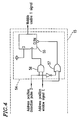
- Figure 4 is a block diagram illustrating a portion of the wobble PLL detection circuit 15
- Figure 5 is a block diagram illustrating a remaining portion of the wobble PLL detection circuit 15 .
- the wobble PLL detection circuit 15 includes a delay 51, a counter 52 , a window generation circuit 53 , and a determination section 54 as shown in Figure 5 .
- the delay 51 adds a fixed amount of delay to the address position detection pulse D generated based on the physical address position, so that a counter 52 is reset by the delayed signal detected by the formatter 8 .
- the reset counter 52 starts counting using the wobble PLL clock F output from the wobble PLL circuit 14 .
- the address position window signal E output from the window generation circuit 53 indicates that the window is opened when it shifts from a low level to a high level, and that the window is closed when it shifts from the high level to the low level.
- the address position window signal E may indicate that the window is opened when it shifts from the high level to the low level, and that the window is closed when it shifts from the low level to the high level.
- the delay 51 and the window generation circuit 53 operate in synchronization with each other by the wobble PLL clock F .
- the delay 51 can delay the address position detection pulse D by X clocks of the wobble PLL clock F .
- the determination section 54 shown in Figure 4 receives the address position detection pulse D and the address position window signal E , so as to determine the state of the wobble PLL clock F .
- the signal output from an AND gate 56 of the determination section 54 shown in Figure 4 becomes a high level.
- the flipflop 55 detects the rising of the signal output from the AND gate 56 , the flipflop 55 sets a wobble usable 1 signal G at a high level.
- the wobble usable 1 signal G When the wobble usable 1 signal G is in a high level, the difference between the length of one sector detected based on the physical address positions and the length of one sector counted with the wobble PLL clock F synchronized by the wobble PLL circuit 14 is within ⁇ 16 clocks. More specifically, if the difference between the reference clock and the counted wobble PLL clock F during the scanning of a sector immediately preceding a sector having a data section providing information for generating the address position detection pulse D is within ⁇ 16 channel clocks, the formatter 8 determines that the wobble PLL clock F generated by the wobble PLL circuit 14 can be used for recording. By this determination, gate signals are generated from the wobble PLL clock F , CLV control is performed based on the wobble PLL clock F , or data is recorded on the optical disk 1 using the wobble PLL clock F as a reference clock.
- Figure 3 shows the respective signals in the case where the address position detection pulse D is not detected while the window is opened.
- the frequency of the wobble PLL clock 7 is higher than that of the actual wobbling.
- the optical disk recording/reproduction apparatus 100 When the optical disk recording/reproduction apparatus 100 is designed so that data is recorded in synchronization with the wobble PLL clock F output from the wobble PLL circuit 14 and the address position detection pulse D is not located within the window, no data recording is performed. Even when data is being sequentially recorded on a predetermined region of a sector, the recording is immediately suspended if the address position detection pulse D is not located within the window.
- the window forming method is employed for detecting a difference between the physical sector cycle by address reproduction and the sector cycle based on the wobble clock.
- the physical sector cycle by address production may be counted with the wobble clock, and the count value may be compared with the regulation value to detect the difference. In this case, also, substantially the same effect can be obtained.
- substantially the same effect as that obtained by the optical disk recording/reproduction apparatus 100 can be obtained by performing the following. That is, the number of wobble clocks to be counted is increased from the number in the case of the above-described optical disk recording/reproduction apparatus, by a number obtained by adding one to the number of sectors interposed between sectors of which addresses have been reproduced, and the cycle between the address positions of the reproduced addresses is used.
- Figure 6 is a block diagram illustrating an optical disk recording/reproduction apparatus 200 of Example 2.
- the optical disk recording/reproduction apparatus 200 includes a wobble signal processing block 60 .
- the construction of the wobble signal processing block 60 is substantially the same as that of the wobble signal processing block 50 of the optical disk recording/reproduction apparatus 100 , except for a wobble PLL detection circuit 15a and a wobble signal failure detection circuit 17 .
- Laser light emitted from the optical head 3 under control of the light amount by the laser driving circuit 16 is reflected from the optical disk 1 which is being rotated by the spindle motor 2 .
- the reflected light from the optical disk 1 is received by a photo detector (not shown) of the optical head 3 , and the output signal is subjected to current-voltage (I-V) conversion by a head amplifier (not shown).
- the I-V converted output signal is received by the operation circuit 4 , which generates a focusing error signal, a tracking error signal, an address reproduced signal, a wobble reproduced signal, a wide-band push-pull tracking error signal A for data reproduction, and a full addition signal.
- the operation circuit 4 outputs the focusing error signal and the tracking error signal to the servo control circuit 5 , the wide-band push-pull tracking error signal and the full addition signal to the reproduced signal processing circuit 6 , and the wide-band push-pull tracking error signal to the polarity selection circuit 11 in the wobble signal processing block 60 .
- the servo control circuit 5 performs focusing servo control for the optical head 3 so that a light spot (not shown) is focused on the recording surface of the optical disk 1 .
- the servo control circuit 5 also performs tracking servo control so that the light spot follows a track of the optical disk 1 (a groove or a land between grooves on the recording surface of the optical disk 1 ). In this operation, assume that the gain in the tracking servo control is sufficiently lower than the frequency of the wobbling of the track of the optical disk 1 and that the tracking servo control does not follow the wobbling.
- the wide-band push-pull tracking error signal A is selected for the ID section, while the full addition signal is selected for the recording section thereof, based on an ID section gate generated by the formatter 8 .
- the reproduced signal processing circuit 6 Upon activation of a lead gate generated by the formatter 8 , the reproduced signal processing circuit 6 performs reproduction PLL for an address and data, and the resultant signal is output to the formatter 8 as digital data.
- the lead gate is activated only for the ID section during the standby state where recording of data on the optical disk 1 is held in readiness and during recording where data is being recorded on the optical disk 1 .
- the lead gate is activated for both the ID section and the data (recording) section.
- the formatter 8 performs demodulation and error checking for signals corresponding to the plurality of physical IDs located at the head of a sector of the digital data reproduced by the reproduced signal processing circuit 6 . Although a delay is generated in the signal processing for reproducing the address, the physical position of the plurality of physical IDs in the sector is detected based on the timing at which the plurality of physical IDs have been reproduced and the ID numbers, and the signal indicating the detected position is output to the wobble PLL detection circuit 15a as an address position detection pulse D .
- the polarity selection circuit 11 of the wobble signal processing block 60 receives the wide-band push-pull tracking error signal output from the operation circuit 4 and a signal indicating the polarity of tracking, i.e., whether the track is a land or a groove, output from the servo control circuit 5 .
- the polarity selection circuit 11 selects the polarity of the signal received from the operation circuit 4 to be output to the bandpass filter 12 based on the signal received from the servo control circuit 5 .
- the bandwidth of the bandpass filter 12 is determined so that recording of data on the optical disk 1 and reproduction of data recorded on the optical disk 1 are possible for different linear velocities.
- the bandpass filter 12 has a bandwidth that is determined considering as a center the standard linear velocity at which a light spot follows a track of the optical disk 1 and the frequency obtained from the cycle of the wobbling of the track originally formed on the optical disk 1 as a basis, so that a wobble signal can pass therethrough reliably even for a linear velocity in a range of a half to double the standard linear velocity.
- the wobble digitizing circuit 13 receives a wobble signal H ( Figure 7 ) output from the bandpass filter 12 and performs analog to digital conversion for the wobble signal H .
- the slice level may be a level offset with respect to the center of an envelope of the wobble signal H output from the bandpass filter 12 , or the slice level may be a level offset with respect to level 0 of the bandpass filter 12 .
- a wobble digitized signal I ( Figure 7 ) is not output from the wobble digitizing circuit 13 , i.e., the wobble digitized signal I is in a low level.
- the wobble digitizing circuit 13 masks the digitized signal corresponding to the ID section and several pulses subsequent to the digitized signal corresponding to the ID section by use of the ID section gate generated by the formatter 8 . Then, the masked signal is output from the wobble digitizing circuit 13 . By this masking, the digitized signal corresponding to the ID section is fixed to a low level.
- the wobble PLL circuit 14 includes a VCO (not shown).
- a signal obtained by dividing a clock from the VCO by N (wherein N is the number of channel clocks in the wobble cycle) is phase-synchronized with the masked wobble digitized signal I output from the wobble digitizing circuit 13 .
- a phase difference signal between the wobble digitized signal I and the N-divided VCO clock is fed back to an input terminal of the VCO via a low-pass filter (not shown).
- the wobble PLL circuit 14 outputs the resultant wobble PLL clock generated by the VCO to the recording pulse generation circuit 7 , the formatter 8 , and the wobble PLL detection circuit 15a .
- the wobble signal failure detection circuit 17 detects a rising edge of the wobble digitized signal I and outputs a wobble failure detection signal when the wobble signal has failed for a predetermined time period.
- the formatter 8 determines based on a wobble usable 2 signal output from the wobble PLL detection circuit 15a , which will be described hereinafter, whether or not it should generate a plurality of gates from the wobble PLL clock generated by the VCO of the wobble PLL circuit 14 , whether or not CLV control based on the wobble PLL clock should be performed, or whether or not data should be recorded on the optical disk 1 based on the wobble PLL clock.
- the RISC processing section 9 When data is to be recorded on the optical disk 1 , the RISC processing section 9 performs at least one of the processings, i.e., addition of an error correction code, interleaving, and scrambling, for data output from the system controller 10 .
- the thus-processed data is output to the formatter 8 and stored in a FIFO memory (not shown) in the formatter 8 .
- the system controller 10 sets a recording target sector for the formatter 8 .
- the formatter 8 modulates data in the FIFO memory, and while adding VFO pattern, SYNC, and the like to the modulated data, outputs the modulated data to the recording pulse generation circuit 7 .
- the recording pulse generation circuit 7 processes the modulated data output from the formatter 8 to produce a pulse light beam for allowing a laser to actually emit light and outputs the pulse light beam to the laser driving circuit 16 , which drives the laser to realize recording data on the optical disk 1 .
- Figure 7 is a view illustrating the wobble signal H , the wobble digitized signal I , and a rising edge detection signal J in the case where a defect, attachment of dust, or the like is generated on the recording section of a sector, preventing the optical disk 1 from reflecting light.
- Figure 8 is a block diagram illustrating the wobble PLL detection circuit 15a .
- the wobble PLL detection circuit 15a includes a counter 61 and a wobble failure detection circuit 62 as a determination section as shown in Figure 8 .
- the wobble digitized signal I digitized with the offset slice level having an offset described above becomes a low level in the portion where the defect or the like has been generated.
- the wobble signal failure detection circuit 17 detects a rising edge of the wobble digitized signal I , and generates the rising edge detection signal J indicating the rising edge of the wobble digitized signal I .
- the rising edge detection signal J is also in a low level.
- the counter 61 is reset every pulse of the rising edge detection signal J generated by the wobble signal failure detection circuit 17 .
- the value of the counter 61 is always equal to or less than a predetermined value.
- the wobble failure detection circuit 62 therefore outputs a low-level signal. This low-level signal is inverted by an inverter 63 , so that the wobble PLL detection circuit 15a outputs a high-level wobble usable 2 signal M .
- the predetermined value mentioned above is a threshold with which a failure of the wobble signal can be determined, which is a count number corresponding to a cycle two or more times the wobble cycle.
- the wobble cycle as used herein indicates a cycle N times the wobble clock or the system reference clock.
- the wobble signal failure detection circuit 17 fails to detect the rising edge of the wobble digitized signal I , and thus the counter 61 is not reset.
- the wobble failure detection circuit 62 outputs a high-level signal. This high-level signal is inverted by the inverter 63 , so that the wobble PLL detection circuit 15a outputs a low-level wobble usable 2 signal M .
- the counter 61 is reset by the rising edge detection signal J , turning the wobble usable 2 signal M to the high level.
- the wobble PLL clock after passing the defect portion fails reliability, once wobble failure is detected, i.e., once the formatter 8 detects that the wobble usable 2 signal M has become a low level, the formatter 8 stops or suspends the recording on the defective sector.
- Example 2 may be combined with Example 1.
- the formatter 8 may receive a signal obtained by calculating logical AND of the wobble usable 1 signal in Example 1 and the wobble usable 2 signal in Example 2, so as to realize both operations of wobble PLL clocking and stopping or suspending recording when a signal fails.
- the determination on whether or not the wobble clock is usable at the start of recording is not limited to the method described in Example 1.
- Example 2 the failure of the wobble signal is detected by digitizing the wobble signal by providing an offset to measure the length of a continuing low level of the signal.
- substantially the same effect as that described in Example 2 can be obtained by measuring the length of a continuing time period during which the amplitude of the wide-band push-pull tracking error signal or the signal having just passed the bandpass filter 12 is equal to or less than a predetermined value.
- Substantially the same effect as that described in Example 2 can also be obtained by integrating the amplitude level of the wide-band push-pull tracking error signal or the signal having just passed the bandpass filter 12 and digitizing the integrated signal with a predetermined value.
- the wobble signal failure detection circuit 17 detects a rising edge of the wobble digitized signal output from the wobble digitizing circuit 13 .
- a falling edge of the wobble digitized signal may be detected.
- Figure 9 is a block diagram illustrating an optical disk recording/reproduction apparatus 300 of Example 3.
- the optical disk recording/reproduction apparatus 300 includes a wobble signal processing block 70 .
- the construction of the wobble signal processing block 70 is substantially the same as that of the wobble signal processing block 50 of the optical disk recording/reproduction apparatus 100 , except for a wobble PLL detection circuit 15b and a wobble signal failure detection circuit 17 .
- Laser light emitted from the optical head 3 under control of the light amount by the laser driving circuit 16 is reflected from the optical disk 1 which is being rotated by the spindle motor 2 .
- the reflected light from the optical disk 1 is received by a photo detector (not shown) of the optical head 3 , and the output signal is subjected to current-voltage (I-V) conversion by a head amplifier (not shown).
- the I-V converted output signal is received by the operation circuit 4 , which generates a focusing error signal, a tracking error signal, an address reproduced signal, a wobble reproduced signal, a wide-band push-pull tracking error signal A for data reproduction, and a full addition signal.
- the operation circuit 4 outputs the focusing error signal and the tracking error signal to the servo control circuit 5 , the wide-band push-pull tracking error signal and the full addition signal to the reproduced signal processing circuit 6 , and the wide-band push-pull tracking error signal to the polarity selection circuit 11 in the wobble signal processing block 70 .
- the servo control circuit 5 performs focusing servo control for the optical head 3 so that a light spot (not shown) is focused on the recording surface of the optical disk 1 .
- the servo control circuit 5 also performs tracking servo control so that the light spot follows a track of the optical disk 1 (a groove or a land between grooves on the recording surface of the optical disk 1 ). In this operation, assume that the gain in the tracking servo control is sufficiently lower than the frequency of the wobbling of the track of the optical disk 1 and that the tracking servo control does not follow the wobbling.
- the wide-band push-pull tracking error signal A is selected for the ID section of a sector of the signal, while the full addition signal is selected for the recording section thereof, based on an ID section gate generated by the formatter 8 .
- the reproduced signal processing circuit 6 Upon activation of a lead gate generated by the formatter 8 , the reproduced signal processing circuit 6 performs reproduction PLL for an address and data, and the resultant signal is output to the formatter 8 as digital data.
- the lead gate is activated only for the ID section during the standby state where recording of data on the optical disk 1 is held in readiness and during recording where data is being recorded on the optical disk 1 .
- the lead gate is activated for both the ID section and the data (recording) section.
- the formatter 8 performs demodulation and error checking for signals corresponding to the plurality of physical IDs located at the head of a sector of the digital data reproduced by the reproduced signal processing circuit 6 . Although a delay is generated in the signal processing for reproducing the address, the physical position of a plurality of physical IDs in the sector is detected based on the timing at which the plurality of physical IDs has been reproduced and the ID numbers, and the signal indicating the detected portion is output to the wobble PLL detection circuit 15b as an address position detection pulse D .
- the polarity selection circuit 11 of the wobble signal processing block 70 receives the wide-band push-pull tracking error signal output from the operation circuit 4 and a signal indicating the polarity of tracking, i.e., whether the track is a land or a groove, output from the servo control circuit 5 .
- the polarity selection circuit 11 selects the polarity of the signal received from the operation circuit 4 to be output to the bandpass filter 12 based on the signal received from the servo control circuit 5 .
- the bandwidth of the bandpass filter 12 is determined so that recording of data on the optical disk 1 and reproduction of data recorded on the optical disk 1 are possible for different linear velocities.
- the bandpass filter 12 has a bandwidth that is determined considering the standard linear velocity at which a light spot follows a track of the optical disk 1 and the frequency obtained from the cycle of the wobbling of the track originally formed on the optical disk 1 as a basis, so that a wobble signal can pass therethrough reliably even for a linear velocity in a range of a half to double the standard linear velocity.
- the wobble digitizing circuit 13 receives the wobble signal output from the bandpass filter 12 and performs analog to digital conversion for the wobble signal.
- the slice level may be a level offset with respect to the center of an envelope of the wobble signal output from the bandpass filter 12 , or the slice level may be a level offset with respect to level 0 of the bandpass filter 12 .
- the wobble digitized signal is not output from the wobble digitizing circuit 13 , i.e., the wobble digitized signal is in a low level.
- the wobble digitizing circuit 13 masks the digitized signal corresponding to the ID section and several pulses subsequent to the digitized signal corresponding to the ID section by use of the ID section gate generated by the formatter 8 . Then, the masked signal is output from the wobble digitizing circuit 13 . By this masking, the digitized signal corresponding to the ID section is fixed to a low level.
- the wobble PLL circuit 14 includes a VCO (not shown).
- a signal obtained by dividing a clock from the VCO by N (wherein N is the number of channel clocks in the wobble cycle) is phase-synchronized with the masked wobble digitized signal output from the wobble digitizing circuit 13 .
- a phase difference signal between the wobble digitized signal and the N-divided VCO clock is fed back to an input terminal of the VCO via a low-pass filter (not shown).
- the wobble PLL circuit 14 outputs the resultant wobble PLL clock generated by the VCO to the recording pulse generation circuit 7 , the formatter 8 and the wobble PLL detection circuit 15b .
- the wobble signal failure detection circuit 17 detects a rising edge of the wobble digitized signal and outputs a wobble failure detection signal when the wobble signal has failed for a predetermined time period.
- the formatter 8 determines, based on a wobble usable 3 signal output from the wobble PLL detection circuit 15b , which will be described hereinafter, whether or not it should generate a plurality of gates from the wobble PLL clock generated by the VCO of the wobble PLL circuit 14 , whether or not CLV control based on the wobble PLL clock should be performed, or whether or not data should be recorded on the optical disk 1 based on the wobble PLL clock.
- the RISC processing section 9 When data is to be recorded on the optical disk 1 , the RISC processing section 9 performs at least one of the processings, i.e., addition of an error correction code, interleaving, and scrambling, for data output from the system controller 10 .
- the thus-processed data is output to the formatter 8 and stored in a FIFO memory (not shown) in the formatter 8 .
- the system controller 10 sets a recording target sector for the formatter 8 .
- the formatter 8 modulates data in the FIFO memory, and while adding signals output from VFO pattern, SYNC, and the like to the modulated data, outputs the modulated data to the recording pulse generation circuit 7 .
- the recording pulse generation circuit 7 processes the modulated data output from the formatter 8 to produce a pulse light beam for allowing a laser to actually emit light and outputs the pulse light beam to the laser driving circuit 16 , which drives the laser to realize recording data on the optical disk 1 .
- Figure 10 is a block diagram illustrating the wobble PLL detection circuit 15b .
- the operation for detecting a failure of the wobble signal is the same as that described in Example 2. That is, if no light is reflected from the recording section of a sector due to a defect, dust, or the like, the signal digitized with a slice level having an offset continues a low level during the scanning of the portion where the defect or the like exists. This causes the rising edge detection signal output from the wobble signal failure detection circuit 17 to continue at a low level.
- the wobble PLL detection circuit 15b includes a counter 71 , a first wobble failure detection circuit 72 , and a second wobble failure detection circuit 73 .
- the PLL detection circuit 15b outputs a wobble PLL hold signal to the wobble PLL circuit 14 when the output from the wobble digitizing circuit 13 is kept in a low level until the count of the output clock from the wobble PLL circuit 14 reaches or exceeds a predetermined value t1 , or outputs the wobble usable 3 signal to the formatter 8 when it is kept in a low level until the count reaches or exceeds a value t2 wherein t2 > t1 .
- the wobble PLL circuit 14 holds a voltage of the signal input to the input terminal of the VCO when the wobble failure detection circuit 17 detects a failure of a signal, i.e., when the wobble PLL hold signal is received, keeping the clock at a fixed level.
- the counter 71 counts the time period during which the rising edge detection signal J shown in Figure 7 is in a low level.
- the first wobble failure detection circuit 72 generates a high-level wobble PLL hold signal when the count value exceeds a threshold L1 .
- the threshold L1 is a value corresponding to the time period t1 during which the wobbling signal fails.
- the second wobble failure detection circuit 73 When the count value exceeds a threshold L2 , the second wobble failure detection circuit 73 generates a high-level signal, and the high-level signal is inverted by an inverter to generate a wobble usable 3 signal which accepts the state where the count value does not exceed the threshold.
- the threshold L2 is a value corresponding to the time period t2 during which the wobbling signal fails.
- Figure 11 is a block diagram illustrating an example of the wobble PLL circuit 14 .
- the input terminal of the VCO of the wobble PLL circuit 14 opens or forms a closed loop depending on the wobble PLL hold signal. If a closed loop is formed, the input voltage at the VCO is controlled based on the phase difference between the wobble digitizing signal and the N-divided wobble clock, so that the wobble digitizing signal and the N-divided wobble clock are phase-synchronized. More specifically, when a wobble failure time period t is less than t1 , the wobble PLL circuit 14 forms a closed loop and performs the normal operation. If t1 ⁇ t ⁇ t2 , the wobble PLL circuit 14 holds an input voltage at the VCO during the time period from t1 to t .
- the wobble PLL circuit 14 holds an input voltage at the VCO during the time period from t1 to t2 . At the moment when the wobble failure time period t reaches t2 , the wobble signal is made unusable and, if data is being recorded, the recording is stopped or suspended.
- the failure of the wobble signal is detected by digitizing the wobble signal by providing an offset to measure the length of a continuing low level of the signal.
- substantially the same effect as that described in this example can be obtained by measuring the length of a continuing time period during which the amplitude of the wide-band push-pull tracking error signal or the signal having just passed the bandpass filter 12 is equal to or less than a predetermined value.
- an optical disk recording apparatus includes: first detection means for detecting a first cycle based on a timing of detection of an ID section of an optical disk; second detection means for detecting a second cycle based on a wobble clock; and determination means for determining the state of the wobble clock based on the first cycle and the second cycle. Accordingly, it is possible to determine whether or not the wobble clock is used for recording data depending on the state of the wobble clock. Also, the optical disk recording apparatus according to the present invention can stop or suspend recording of data on the optical disk if the state of the wobble clock is not good.
- Another optical disk recording apparatus records data on an optical disk having tracks wobbled in the radial direction at a predetermined cycle, by phase-synchronizing the cycle of the wobbling and an N-divided wobble clock (wherein N is a rational number) so that the data recording is synchronous with the wobble clock.
- the optical disk recording apparatus is provided with detection means for detecting a failure of the wobble signal. In this optical disk recording apparatus according to the present invention, when a portion of the wobble signal has failed, data recording can be stopped or suspended.
Abstract
Description
- The present invention relates to a rewritable optical disk recording apparatus and a method for recording data on a rewritable optical disk.
- A DVD-RAM (digital versatile disk random access memory) has sectors each composed of an ID section including four physical identifications (IDs) and a recording section which data is recorded on and/or reproduced from. Figure 12 illustrates an exemplified format of such a DVD-RAM. In the recording section, tracks wobble in the radial direction forming sine shapes at a cycle of 186 channel clocks, so that this wobbling of tracks is observed in a push-pull tracking error signal as a wobble signal. Specifically, as shown in Figure 2, a wobble signal is observed in the portion of a wide-band push-pull tracking error signal corresponding to the recording section.
- The above wobble signal is allowed to pass through a narrow-band bandpass filter to digitize the wobble signal. The digitized signal and a signal obtained by dividing an oscillating frequency of a voltage controlled oscillator (VCO) by 186 are phase-compared. The resultant phase difference signal is allowed to pass through a low pass filter and then returned to an input of the VCO, so as to constitute a phase locked loop (PLL) (hereinafter, such a PLL is called a wobble PLL), thereby to achieve phase-synchronization. As a result, the oscillation clock from the VCO serves as a channel clock frequency of a physical disk. By using the oscillation clock from the VCO as a recording reference clock for recording and reproduction of data, data can be recorded on the disk substantially in synchronization with the sectors of the disk.
- When data is recorded on or reproduced from a disk using a fixed clock from a crystal oscillator, a synthesizer, or the like as a reference clock, the data recording or reproduction is directly influenced by variation factors such as a shift of the fixed clock, a variation in the rotation of a spindle motor, and a variation in the linear velocity due to eccentricity of the disk. When recording of data is influenced by any of such factors, it may become impossible to correctly reproduce the data written on the disk. In some cases, when recording of data is influenced by any of such factors, data may be written on the physical IDs, failing to read information originally written on the physical IDs.
- On the contrary, when the wobble PLL clock described above is used for data recording, since the wobble PLL clock follows a variation in the rotation of a spindle motor and a variation in the linear velocity due to eccentricity of a disk, data which has absorbed all of the variation factors can be recorded.
- However, if such a wobble PLL clock fails to be synchronous with the wobbling on the disk, using the wobble PLL clock as a reference clock may cause a problem, data may fail to be reproduced, or may be written on physical IDs.
- As another problem, when a disk is defective, has dust attached, or poorly reflects light, a tracking error signal is not generated. This means that the wobble PLL clock loses one object for comparison, and thus the reliability of the clock itself is lost.
- The optical disk recording apparatus of this invention includes: a first detection section for detecting a first cycle based on a timing of detection of an ID section of an optical disk; a second detection section for detecting a second cycle based on a wobble clock; and a state determination section for determining a state of the wobble clock based on the first cycle and the second cycle.
- In one embodiment of the invention, the optical disk recording apparatus further includes a use determination section for detecting whether or not the wobble clock is usable based on the state of the wobble clock.
- In another embodiment of the invention, the state determination section generates a window based on the first cycle and determines the state of the wobble clock depending on whether or not a signal indicating the second cycle exists within the window, and the use determination section determines that the wobble clock is usable when the signal indicating the second cycle exists within the window.
- In still another embodiment of the invention, the optical disk recording apparatus further includes a recording section for recording data, and recording stop/suspension determination section for determining whether or not the recording should be stopped/ suspended based on the state of the wobble clock.
- In still another embodiment of the invention, the state determination section generates a window based on the first cycle and determines the state of the wobble clock depending on whether or not a signal indicating the second cycle exists within the window, and the stop/suspension determination section stops/suspends the recording when the signal indicating the second cycle exists outside the window.
- Alternatively, the optical disk recording apparatus of this invention is for recording data on an optical disk having a track wobbled in a radial direction at a predetermined cycle in synchronization with a wobble clock by phase-synchronizing the cycle of the wobbling and an N-divided wobble clock (wherein N is a rational number). The optical disk recording apparatus includes: a failure determination section for determining whether or not a wobble signal has failed.
- In one embodiment of the invention, the optical disk recording apparatus further includes a use determination section for determining whether or not the wobble clock is usable when the failure determination section determines that the wobble signal has failed.
- In another embodiment of the invention, the optical disk recording apparatus reproduces the wobble signal recorded on the optical disk, and generates a digitized signal obtained by digitizing the reproduced wobble signal when the reproduced wobble signal has an amplitude equal to or more than a predetermined value, and the failure determination section determines that the wobble signal has failed when the digitized signal is not output for a predetermined time period.
- In still another embodiment of the invention, the optical disk recording apparatus further includes a recording section for recording data, and a recording stop/suspension determination section for determining whether or not the recording should be stopped/suspended depending on the failure of the wobble signal.
- In still another embodiment of the invention, the optical disk recording apparatus reproduces the wobble signal recorded on the optical disk, and generates a digitized signal obtained by digitizing the reproduced wobble signal when the reproduced wobble signal has an amplitude equal to or more than a predetermined value, the failure determination section determines that the wobble signal has failed when the digitized signal is not output for a predetermined time period, and the recording stop/suspension determination section stops/suspends the recording when the failure determination section determines that the wobble signal has failed.
- In still another embodiment of the invention, the optical disk recording apparatus hold the wobble clock when the failure determination section determines that the wobble signal has failed for a predetermined time t1, and the optical disk recording apparatus makes the wobble clock unusable when the failure determination section determines that the wobble signal has failed for a predetermined time t2.
- Alternatively, the optical disk recording apparatus of this invention includes: a wobble reproduced signal processing section for reproducing a wobble signal to output a reproduced signal; a digitizing section which does not output a digitized signal obtained by digitizing the reproduced signal when the reproduced signal has an amplitude less than a predetermined value or outputs the digitized signal when the reproduced signal has an amplitude equal to or more than the predetermined value; a first failure determination section for outputting a first failure signal when the digitized signal is not output for a predetermined time period t1; a second failure determination section for outputting a second failure signal when the digitized signal is not output for a predetermined time period t2; a wobble phase difference detection section for outputting a phase difference signal between the digitized signal output from the digitizing section and an N-divided output clock output from a VCO; a wobble PLL section for passing the phase difference signal output from the wobble phase difference detection section to the VCO via a low-pass filter; a PLL blocking section for blocking the wobble PLL section from passing the phase difference signal to the VCO, depending on the first failure signal; and a wobble clock usable determination section for determining whether or not the wobble clock is usable depending on the second failure signal.
- In one embodiment of the invention, the optical disk recording apparatus holds the wobble clock when the failure determination section determines that the wobble signal has failed for a predetermined time t1, and the optical disk recording apparatus stops/suspends recording of information when the failure determination section determines that the wobble signal has failed for a predetermined time t2.
- In another embodiment of the invention, the predetermined time t2 is longer than the predetermined time t1.
- In still another embodiment of the invention, the predetermined time t2 is equal to or longer than the predetermined time t1.
- Alternatively, the optical disk recording apparatus of this invention includes: a wobble reproduced signal processing section for reproducing a wobble signal to output a reproduced signal; a digitizing section which does not output a digitized signal obtained by digitizing the reproduced signal when the reproduced signal has an amplitude less than a predetermined value or outputs the digitized signal when the reproduced signal has an amplitude equal to or more than the predetermined value; a first failure determination section for outputting a first failure signal when the digitized signal is not output for a predetermined time period t1; a second failure determination section for outputting a second failure signal when the digitized signal is not output for a predetermined time period t2; a wobble phase difference detection section for outputting a phase difference signal between the digitized signal output from the digitizing section and an N-divided output clock output from a VCO; a wobble PLL section for passing the phase difference signal output from the wobble phase difference detection section to the VCO via a low-pass filter; a PLL blocking section for blocking the wobble PLL section from passing the phase difference signal to the VCO, depending on the first failure signal; and a stop/suspension section for stopping/suspending recording of information on the optical disk during the recording depending on the second failure signal.
- According to another aspect of the invention, a method for recording data on an optical disk is provided. The method includes the steps of: detecting a first cycle based on a timing of detection of an ID section of the optical disk; detecting a second cycle based on a wobble clock; and determining a state of the wobble clock based on the first cycle and the second cycle.
- In one embodiment of the invention, the method for recording data on an optical disk further includes the step of determining whether or not the wobble clock is usable based on the state of the wobble clock.
- In another embodiment of the invention, the step of determining a state of the wobble clock generates a window based on the first cycle and determines the state of the wobble clock depending on whether or not a signal indicating the second cycle is within the window, and the step of determining whether or not the wobble clock is usable determines that the wobble clock is usable when the signal indicating the second cycle is within the window.
- In still another embodiment of the invention, the method for recording data on an optical disk further includes the steps of: recording data; and stopping/suspending the recording based on the state of the wobble clock.
- In still another embodiment of the invention, the step of determining a state of the wobble clock generates a window based on the first cycle and determines the state of the wobble clock depending on whether or not a signal indicating the second cycle is within the window, and the step of stopping/suspending the recording stops/suspends the recording when the signal indicating the second cycle is outside the window.
- Alternatively, the method for recording data on an optical disk of this invention includes recording data on the optical disk having a track wobbled in a radial direction at a predetermined period in synchronization with a wobble clock by phase-synchronizing the cycle of the wobbling and an N-divided wobble clock (wherein N is a rational number). The method further includes the step of: determining whether or not a wobble signal has failed.
- In one embodiment of the invention, the method for recording data on an optical disk further includes the step of: determining whether or not the wobble clock is usable when the step of determining whether or not a wobble signal has failed determines that the wobble signal has failed.
- In another embodiment of the invention, the method for recording data on an optical disk further includes the steps of: recording data; and stopping/suspending the recording when the wobble signal has failed.
- The "stopping/suspending" as used herein indicates that either one of stopping and suspending is performed.
- Thus, the optical disk recording/reproduction apparatus according to the present invention records data on an optical disk having a plurality of sectors each composed of an ID section formed of prepits and a data section for data recording/reproduction having tracks wobbled in the radial direction at a predetermined cycle, in synchronization with a reference clock obtained by phase-synchronizing the cycle of the wobbling and an N-divided clock (wherein N is a natural number)(hereinafter, such a reference clock is called a wobble clock). The wobble clock is made usable if the difference between the sector cycle determined by reproduction of the physical ID and the sector cycle determined by counting the wobble clock is within a predetermined range, or made unusable if it is not within the predetermined range.
- Alternatively, in the optical disk recording/reproduction apparatus according to the present invention which records and/or reproduces data on and/or from an optical disk having tracks wobbled in the radial direction at a predetermined cycle in synchronization with the wobble clock, the wobble clock is made unusable if the wobble signal fails for a predetermined time period.
- Alternatively, in the optical disk recording/reproduction apparatus according to the present invention which records and/or reproduces data on and/or from an optical disk having tracks wobbled in the radial direction at a predetermined cycle in synchronization with the wobble clock, recording is stopped or suspended if the wobble signal has failed for a predetermined time period during the recording.
- Alternatively, in the optical disk recording/reproduction apparatus according to the present invention which records and/or reproduces data on and/or from an optical disk having tracks wobbled in the radial direction at a predetermined cycle in synchronization with the wobble clock, the wobble clock is held if the wobble signal has failed for a predetermined time period t1, or the wobble clock is made unusable if it has failed for a predetermined time period t2 wherein t2 > t1.
- Alternatively, in the optical disk recording/reproduction apparatus according to the present invention which records and/or reproduces data on and/or from an optical disk having tracks wobbled in the radial direction at a predetermined cycle in synchronization with the wobble clock, the wobble clock is held if a portion of the wobble signal has failed for a predetermined time period t1, or recording is stopped or suspended if the wobble signal has failed for a predetermined t2 wherein t2 > t1 during the recording.
- Thus, the invention described herein makes possible the advantages of providing (1) an optical disk recording apparatus and (2) recording data on an optical disk, in which the state of a wobble signal is determined and recording of data on an optical disk is suspended or stopped if the state of the wobble signal does not satisfy predetermined conditions, so as to realize stable recording of data on the optical disk.
- These and other advantages of the present invention will become apparent to those skilled in the art upon reading and understanding the following detailed description with reference to the accompanying figures.
-
- Figure 1 is a block diagram illustrating an optical disk recording/reproduction apparatus of Example 1 according to the present invention;
- Figure 2 is a view illustrating a wide-band push-pull tracking error signal A, a wobble digitized signal B, a wobble PLL clock N-divided signal C, an address position detection pulse D, an address position window signal E, and a wobble PLL clock F, in a wobble usable state;
- Figure 3 is a view illustrating a wide-band push-pull tracking error signal A, a wobble digitized signal B, a wobble PLL clock N-divided signal C, an address position detection pulse D, an address position window signal E, and a wobble PLL clock F, in a wobble unusable state;
- Figure 4 is a view illustrating a portion of a wobble PLL detection circuit of Example 1 according to the present invention;
- Figure 5 is a view illustrating a remaining portion of the wobble PLL detection circuit of Example 1 according to the present invention;
- Figure 6 is a block diagram illustrating an optical disk recording/reproduction apparatus of Example 2 according to the present invention;
- Figure 7 is a view illustrating a wobble signal H, a wobble digitized signal I, and a rising edge detection signal J, when a defect exists on an optical disk;
- Figure 8 is a view illustrating a wobble PLL detection circuit of Example 2 according to the present invention;
- Figure 9 is a block diagram illustrating an optical disk recording/reproduction apparatus of Example 3 according to the present invention;
- Figure 10 is a view illustrating a wobble PLL detection circuit of Example 3 according to the present invention;
- Figure 11 is a view illustrating a wobble PLL circuit of Example 3 according to the present invention; and
- Figure 12 is a view illustrating an example of a DVD-RAM format.
-
- Example 1 according to the present invention will be described with reference to the relevant drawings.
- Figure 1 is a block diagram illustrating an optical disk recording/
reproduction apparatus 100 of Example 1. - The optical disk recording/
reproduction apparatus 100 includes a wobblesignal processing block 50. The wobblesignal processing block 50 detects a first cycle based on the detection timing at an ID section of anoptical disk 1, detects a second cycle based on a wobble clock, and determines the state of the wobble clock based on the first cycle and the second cycle. The optical disk recording/reproduction apparatus 100 may further include aspindle motor 2 for rotating theoptical disk 1, anoptical head 3, an operation circuit 4, a servo control circuit 5, a reproducedsignal processing circuit 6, a recording pulse generation circuit 7, aformatter 8, a reduced instruction set computer (RISC)processing section 9, asystem controller 10, and alaser driving circuit 16. - The wobble
signal processing block 50 includes a wobblePLL detection circuit 15. The wobblesignal processing block 50 may further include apolarity selection circuit 11, abandpass filter 12, awobble digitizing circuit 13, and awobble PLL circuit 14. - Hereinbelow, the operation of the optical disk recording/
reproduction apparatus 100 will be described with reference to Figures 1 to 3. Figures 2 and 3 are views each illustrating a wide-band push-pull tracking error signal A, a wobble digitized signal B, a wobble PLL clock N-divided signal C (N is a rational number), an address position detection pulse D, an address position window signal E, and a wobble PLL clock F. - Laser light emitted from the
optical head 3 under control of the light amount by thelaser driving circuit 16 is reflected from theoptical disk 1 which is being rotated by thespindle motor 2. The reflected light from theoptical disk 1 is received by a photo detector (not shown) of theoptical head 3, and the output signal is subjected to current-voltage (I-V) conversion by a head amplifier (not shown). The I-V converted output signal is received by the operation circuit 4, which generates a focusing error signal, a tracking error signal, an address reproduced signal, the wobble reproduced signal, a wide-band push-pull tracking error signal A for data reproduction, and a full addition signal. - The operation circuit 4 outputs the focusing error signal and the tracking error signal to the servo control circuit 5, the wide-band push-pull tracking error signal A and the full addition signal to the reproduced
signal processing circuit 6, and the wide-band push-pull tracking error signal A to thepolarity selection circuit 11 in the wobblesignal processing block 50. - The servo control circuit 5 performs focusing servo control for the
optical head 3 so that a light spot (not shown) is focused on the recording surface of theoptical disk 1. The servo control circuit 5 also performs tracking servo control so that the light spot follows a track of the optical disk 1 (a groove or a land between grooves on the recording surface of the optical disk 1). In this operation, assume that the gain of the tracking servo control is sufficiently lower than the frequency of the wobbling of the track of theoptical disk 1 and that the tracking servo control does not follow the wobbling. - In the reproduced
signal processing circuit 6, the wide-band push-pull tracking error signal A is selected for the ID section, while the full addition signal is selected for the recording section, based on an ID section gate generated by theformatter 8. Upon activation of a lead gate generated by theformatter 8, the reproducedsignal processing circuit 6 performs synchronization of addresses and data with clocks extracted by reproduction PLL control based on the addresses and data, and the results are output to theformatter 8 as digital data. - In a DVD-RAM, for example, the push-pull signal is used for reproduction of the ID section while the full addition signal is used for reproduction of data. Therefore, switching between these signals is required when the reproduction circuit is shared. The ID section gate is a signal used for this switching. The ID section gate is active during the address period. For example, referring to Figure 2, the ID section gate is in a high level during the period of the ID section and in a low level during the period of the recording section.
- Referring to Figure 12, no object to be reproduced exists between the reproduction of the upper two physical IDs and the reproduction of the lower two physical IDs and between the address reproduction and the data reproduction. If PLL control is attempted when no object to be reproduced exists, a target value determined by the PLL control is diverged, which may result in a failure to correctly perform subsequent address reproduction or data reproduction. In such a case, therefore, the PLL control is preferably stopped (suspended). The lead gate is a signal used to stop (suspend) the PLL control. The lead gate specifies the period during which the PLL control should be performed.
- The lead gate is activated only for the ID section during the standby state where recording of data on the
optical disk 1 is held in readiness and during recording where data is being recorded on theoptical disk 1. During reproduction where data recorded on theoptical disk 1 is being reproduced, the lead gate is activated for both the ID section and the data (recording) section. - The
formatter 8 performs demodulation and error checking for signals corresponding to the plurality of physical IDs located at the head of a sector in the digital data reproduced by the reproducedsignal processing circuit 6. Although a delay is generated in the signal processing for reproducing an address, the physical position of the plurality of physical IDs in the sector is detected based on the timing at which the plurality of physical IDs have been reproduced and the ID numbers, and the signal indicating the detected position is output to the wobblePLL detection circuit 15 as an address position detection pulse D. - The
polarity selection circuit 11 of the wobblesignal processing block 50 receives the wide-band push-pull tracking error signal A output from the operation circuit 4 and a signal indicating the polarity of tracking, i.e., whether the track is a land or a groove, output from the servo control circuit 5. Thepolarity selection circuit 11 selects the polarity of the signal received from the operation circuit 4 to be output to thebandpass filter 12 based on the signal received from the servo control circuit 5. - The bandwidth of the
bandpass filter 12 is determined so that recording of data on theoptical disk 1 and reproduction of data recorded on theoptical disk 1 are possible for different linear velocities. Specifically, thebandpass filter 12 has a bandwidth that is determined considering the standard linear velocity at which a light spot follows a track of theoptical disk 1 and the frequency obtained from the cycle of the wobbling of the track originally formed on theoptical disk 1 as a basis, so that a wobble signal can pass therethrough reliably even for a linear velocity in a range of a half to double the standard linear velocity. - The
wobble digitizing circuit 13 receives the signal output from thebandpass filter 12 and performs analog to digital conversion for the received signal to output the wobble digitized signal B. During this digitization, thewobble digitizing circuit 13 masks the ID section and several pulses subsequent to the ID section of the digitized signal by use of the ID section gate generated by theformatter 8 before outputting the wobble digitized signal B. By this masking, the ID section of the digitized signal is fixed to a low level. - The
wobble PLL circuit 14 includes a voltage controlled oscillator (VCO; not shown). A signal obtained by dividing a clock output from the VCO by N (wherein N is the number of channel clocks in the wobble cycle) is phase-synchronized with the masked wobble digitized signal received from thewobble digitizing circuit 13. In order to achieve this, a phase difference signal between the wobble digitized signal and the N-divided VCO clock is fed back to an input terminal of the VCO via a low-pass filter (not shown). Thewobble PLL circuit 14 outputs the resultant wobble PLL clock F generated by the VCO to the recording pulse generation circuit 7, theformatter 8, and the wobblePLL detection circuit 15. - The
formatter 8 determines, based on a wobble usable 1 signal output from the wobblePLL detection circuit 15, which will be described hereinafter, whether or not it should generate a plurality of gates from the wobble PLL clock F generated by the VCO of thewobble PLL circuit 14, whether or not constant linear velocity (CLV) control based on the wobble PLL clock F should be performed, or whether or not data should be recorded on the optical disk based on the wobble PLL clock F. The produced gates are used for recording and reproduction of data and the like. - When data is to be recorded on the
optical disk 1, theRISC processing section 9 performs at least one of the processings, i.e., addition of an error correction code, interleaving, and scrambling, for data output from thesystem controller 10. The thus-processed data is output to theformatter 8 and stored in a FIFO (first in first out) memory (not shown) in theformatter 8. - The
system controller 10 sets a recording target sector for theformatter 8. When reaching the recording target sector during reproduction of addresses, theformatter 8 modulates data in the FIFO memory, and while adding a pattern of a variable frequency oscillator (VFO), a synchronous code (SYNC), and the like to the modulated data, outputs the modulated data to the recording pulse generation circuit 7. The recording pulse generation circuit 7 processes the modulated data output from theformatter 8 to produce a pulse light beam for allowing a laser to actually emit light and outputs the pulse light beam to thelaser driving circuit 16, which drives the laser to realize recording data on theoptical disk 1. - Hereinbelow, the detailed construction and operation of the wobble
PLL detection circuit 15 will be described with reference to Figures 4 and 5. Figure 4 is a block diagram illustrating a portion of the wobblePLL detection circuit 15, and Figure 5 is a block diagram illustrating a remaining portion of the wobblePLL detection circuit 15. - The wobble
PLL detection circuit 15 includes a delay 51, a counter 52, awindow generation circuit 53, and adetermination section 54 as shown in Figure 5. - The delay 51 adds a fixed amount of delay to the address position detection pulse D generated based on the physical address position, so that a counter 52 is reset by the delayed signal detected by the
formatter 8. The reset counter 52 starts counting using the wobble PLL clock F output from thewobble PLL circuit 14. For example, assume that one sector of theoptical disk 1 includes 43152 channel clocks, the delay amount of the delay 51 is one channel clock, and the tolerance of the wobble PLL clock F is ±16 channel clocks. In this case, thewindow generation circuit 53 opens a window when the value of the counter 52 reaches 43135 (= 43152 - 16 - 1) and closes the window when it reaches 43167 (= 43152 + 16 - 1). In this example, the address position window signal E output from thewindow generation circuit 53 indicates that the window is opened when it shifts from a low level to a high level, and that the window is closed when it shifts from the high level to the low level. Alternatively, the address position window signal E may indicate that the window is opened when it shifts from the high level to the low level, and that the window is closed when it shifts from the low level to the high level. - The delay 51 and the
window generation circuit 53 operate in synchronization with each other by the wobble PLL clock F. In this regard, the delay 51 can delay the address position detection pulse D by X clocks of the wobble PLL clock F. - The
determination section 54 shown in Figure 4 receives the address position detection pulse D and the address position window signal E, so as to determine the state of the wobble PLL clock F. When the address position detection pulse D is detected while the window is opened as shown in Figure 2, the signal output from an ANDgate 56 of thedetermination section 54 shown in Figure 4 becomes a high level. When aflipflop 55 detects the rising of the signal output from the ANDgate 56, theflipflop 55 sets a wobble usable 1 signal G at a high level. - When the wobble usable 1 signal G is in a high level, the difference between the length of one sector detected based on the physical address positions and the length of one sector counted with the wobble PLL clock F synchronized by the
wobble PLL circuit 14 is within ±16 clocks. More specifically, if the difference between the reference clock and the counted wobble PLL clock F during the scanning of a sector immediately preceding a sector having a data section providing information for generating the address position detection pulse D is within ±16 channel clocks, theformatter 8 determines that the wobble PLL clock F generated by thewobble PLL circuit 14 can be used for recording. By this determination, gate signals are generated from the wobble PLL clock F, CLV control is performed based on the wobble PLL clock F, or data is recorded on theoptical disk 1 using the wobble PLL clock F as a reference clock. - Figure 3 shows the respective signals in the case where the address position detection pulse D is not detected while the window is opened. In the case shown in Figure 3, the frequency of the wobble PLL clock 7 is higher than that of the actual wobbling.
- In the above case, since the address position detection pulse D is not located within the window, a signal output from an
OR gate 57 of thedetermination section 54 becomes a low level at the moment when the address position detection pulse D is generated. This clears theflipflop 55, thereby setting the wobble usable 1 signal G at a low level. In this case, gate signals are not generated from the wobble PLL clock F, CLV control is not performed based on the wobble PLL clock F, and/or data is not recorded on theoptical disk 1 using the wobble PLL clock F as a reference clock. - When the optical disk recording/
reproduction apparatus 100 is designed so that data is recorded in synchronization with the wobble PLL clock F output from thewobble PLL circuit 14 and the address position detection pulse D is not located within the window, no data recording is performed. Even when data is being sequentially recorded on a predetermined region of a sector, the recording is immediately suspended if the address position detection pulse D is not located within the window. - In this example, the window forming method is employed for detecting a difference between the physical sector cycle by address reproduction and the sector cycle based on the wobble clock. Alternatively, the physical sector cycle by address production may be counted with the wobble clock, and the count value may be compared with the regulation value to detect the difference. In this case, also, substantially the same effect can be obtained.
- In the case where the address of one sector in a sequence of sectors fail to be reproduced, for example, in the case where the sector cycle of one sector fails to be determined, substantially the same effect as that obtained by the optical disk recording/
reproduction apparatus 100 can be obtained by performing the following. That is, the number of wobble clocks to be counted is increased from the number in the case of the above-described optical disk recording/reproduction apparatus, by a number obtained by adding one to the number of sectors interposed between sectors of which addresses have been reproduced, and the cycle between the address positions of the reproduced addresses is used. - Example 2 according to the present invention will be described with reference to the relevant drawings.
- Figure 6 is a block diagram illustrating an optical disk recording/
reproduction apparatus 200 of Example 2. - The optical disk recording/
reproduction apparatus 200 includes a wobblesignal processing block 60. The construction of the wobblesignal processing block 60 is substantially the same as that of the wobblesignal processing block 50 of the optical disk recording/reproduction apparatus 100, except for a wobblePLL detection circuit 15a and a wobble signalfailure detection circuit 17. - Laser light emitted from the
optical head 3 under control of the light amount by thelaser driving circuit 16 is reflected from theoptical disk 1 which is being rotated by thespindle motor 2. The reflected light from theoptical disk 1 is received by a photo detector (not shown) of theoptical head 3, and the output signal is subjected to current-voltage (I-V) conversion by a head amplifier (not shown). The I-V converted output signal is received by the operation circuit 4, which generates a focusing error signal, a tracking error signal, an address reproduced signal, a wobble reproduced signal, a wide-band push-pull tracking error signal A for data reproduction, and a full addition signal. - The operation circuit 4 outputs the focusing error signal and the tracking error signal to the servo control circuit 5, the wide-band push-pull tracking error signal and the full addition signal to the reproduced
signal processing circuit 6, and the wide-band push-pull tracking error signal to thepolarity selection circuit 11 in the wobblesignal processing block 60. - The servo control circuit 5 performs focusing servo control for the
optical head 3 so that a light spot (not shown) is focused on the recording surface of theoptical disk 1. The servo control circuit 5 also performs tracking servo control so that the light spot follows a track of the optical disk 1 (a groove or a land between grooves on the recording surface of the optical disk 1). In this operation, assume that the gain in the tracking servo control is sufficiently lower than the frequency of the wobbling of the track of theoptical disk 1 and that the tracking servo control does not follow the wobbling. - In the reproduced
signal processing circuit 6, the wide-band push-pull tracking error signal A is selected for the ID section, while the full addition signal is selected for the recording section thereof, based on an ID section gate generated by theformatter 8. Upon activation of a lead gate generated by theformatter 8, the reproducedsignal processing circuit 6 performs reproduction PLL for an address and data, and the resultant signal is output to theformatter 8 as digital data. - The lead gate is activated only for the ID section during the standby state where recording of data on the
optical disk 1 is held in readiness and during recording where data is being recorded on theoptical disk 1. During reproduction where data recorded on theoptical disk 1 is being reproduced, the lead gate is activated for both the ID section and the data (recording) section. - The
formatter 8 performs demodulation and error checking for signals corresponding to the plurality of physical IDs located at the head of a sector of the digital data reproduced by the reproducedsignal processing circuit 6. Although a delay is generated in the signal processing for reproducing the address, the physical position of the plurality of physical IDs in the sector is detected based on the timing at which the plurality of physical IDs have been reproduced and the ID numbers, and the signal indicating the detected position is output to the wobblePLL detection circuit 15a as an address position detection pulse D. - The
polarity selection circuit 11 of the wobblesignal processing block 60 receives the wide-band push-pull tracking error signal output from the operation circuit 4 and a signal indicating the polarity of tracking, i.e., whether the track is a land or a groove, output from the servo control circuit 5. Thepolarity selection circuit 11 selects the polarity of the signal received from the operation circuit 4 to be output to thebandpass filter 12 based on the signal received from the servo control circuit 5. - The bandwidth of the
bandpass filter 12 is determined so that recording of data on theoptical disk 1 and reproduction of data recorded on theoptical disk 1 are possible for different linear velocities. Specifically, thebandpass filter 12 has a bandwidth that is determined considering as a center the standard linear velocity at which a light spot follows a track of theoptical disk 1 and the frequency obtained from the cycle of the wobbling of the track originally formed on theoptical disk 1 as a basis, so that a wobble signal can pass therethrough reliably even for a linear velocity in a range of a half to double the standard linear velocity. - The
wobble digitizing circuit 13 receives a wobble signal H (Figure 7) output from thebandpass filter 12 and performs analog to digital conversion for the wobble signal H. In the digitization of the wobble signal H output from thebandpass filter 12, the slice level may be a level offset with respect to the center of an envelope of the wobble signal H output from thebandpass filter 12, or the slice level may be a level offset with respect to level 0 of thebandpass filter 12. For example, when the amplitude of the wobble signal is small, a wobble digitized signal I (Figure 7) is not output from thewobble digitizing circuit 13, i.e., the wobble digitized signal I is in a low level. - During the above digitization, the
wobble digitizing circuit 13 masks the digitized signal corresponding to the ID section and several pulses subsequent to the digitized signal corresponding to the ID section by use of the ID section gate generated by theformatter 8. Then, the masked signal is output from thewobble digitizing circuit 13. By this masking, the digitized signal corresponding to the ID section is fixed to a low level. - The
wobble PLL circuit 14 includes a VCO (not shown). A signal obtained by dividing a clock from the VCO by N (wherein N is the number of channel clocks in the wobble cycle) is phase-synchronized with the masked wobble digitized signal I output from thewobble digitizing circuit 13. In order to achieve this, a phase difference signal between the wobble digitized signal I and the N-divided VCO clock is fed back to an input terminal of the VCO via a low-pass filter (not shown). Thewobble PLL circuit 14 outputs the resultant wobble PLL clock generated by the VCO to the recording pulse generation circuit 7, theformatter 8, and the wobblePLL detection circuit 15a. - The wobble signal
failure detection circuit 17 detects a rising edge of the wobble digitized signal I and outputs a wobble failure detection signal when the wobble signal has failed for a predetermined time period. - The
formatter 8 determines based on a wobble usable 2 signal output from the wobblePLL detection circuit 15a, which will be described hereinafter, whether or not it should generate a plurality of gates from the wobble PLL clock generated by the VCO of thewobble PLL circuit 14, whether or not CLV control based on the wobble PLL clock should be performed, or whether or not data should be recorded on theoptical disk 1 based on the wobble PLL clock. - When data is to be recorded on the
optical disk 1, theRISC processing section 9 performs at least one of the processings, i.e., addition of an error correction code, interleaving, and scrambling, for data output from thesystem controller 10. The thus-processed data is output to theformatter 8 and stored in a FIFO memory (not shown) in theformatter 8. - The
system controller 10 sets a recording target sector for theformatter 8. When reaching the recording target sector during reproduction of addresses, theformatter 8 modulates data in the FIFO memory, and while adding VFO pattern, SYNC, and the like to the modulated data, outputs the modulated data to the recording pulse generation circuit 7. The recording pulse generation circuit 7 processes the modulated data output from theformatter 8 to produce a pulse light beam for allowing a laser to actually emit light and outputs the pulse light beam to thelaser driving circuit 16, which drives the laser to realize recording data on theoptical disk 1. - Hereinbelow, the detailed construction and operation of the wobble
PLL detection circuit 15a will be described with reference to Figures 7 and 8. Figure 7 is a view illustrating the wobble signal H, the wobble digitized signal I, and a rising edge detection signal J in the case where a defect, attachment of dust, or the like is generated on the recording section of a sector, preventing theoptical disk 1 from reflecting light. Figure 8 is a block diagram illustrating the wobblePLL detection circuit 15a. - The wobble
PLL detection circuit 15a includes acounter 61 and a wobblefailure detection circuit 62 as a determination section as shown in Figure 8. - In the case where a defect, attachment of dust, or the like is generated on the recording section of a sector preventing the
optical disk 1 from reflecting light, the wobble digitized signal I digitized with the offset slice level having an offset described above becomes a low level in the portion where the defect or the like has been generated. The wobble signalfailure detection circuit 17 detects a rising edge of the wobble digitized signal I, and generates the rising edge detection signal J indicating the rising edge of the wobble digitized signal I. When the wobble digitized signal I is in the low level, the rising edge detection signal J is also in a low level. - The
counter 61 is reset every pulse of the rising edge detection signal J generated by the wobble signalfailure detection circuit 17. When the rising edge of the wobble digitized signal I is detected at a predetermined wobble cycle, the value of thecounter 61 is always equal to or less than a predetermined value. The wobblefailure detection circuit 62 therefore outputs a low-level signal. This low-level signal is inverted by aninverter 63, so that the wobblePLL detection circuit 15a outputs a high-level wobble usable 2 signal M. - The predetermined value mentioned above is a threshold with which a failure of the wobble signal can be determined, which is a count number corresponding to a cycle two or more times the wobble cycle. The wobble cycle as used herein indicates a cycle N times the wobble clock or the system reference clock.
- When a defect or dust exists on the
optical disk 1, the wobble signalfailure detection circuit 17 fails to detect the rising edge of the wobble digitized signal I, and thus thecounter 61 is not reset. When the value of thecounter 61 becomes or exceeds the predetermined value, the wobblefailure detection circuit 62 outputs a high-level signal. This high-level signal is inverted by theinverter 63, so that the wobblePLL detection circuit 15a outputs a low-level wobble usable 2 signal M. - After the optical spot has passed the defect portion, the
counter 61 is reset by the rising edge detection signal J, turning the wobble usable 2 signal M to the high level. However, since the wobble PLL clock after passing the defect portion fails reliability, once wobble failure is detected, i.e., once theformatter 8 detects that the wobble usable 2 signal M has become a low level, theformatter 8 stops or suspends the recording on the defective sector. - Thus, in this example, it is possible to prevent erroneous recording due to failure of the wobble PLL clock which may occur when the wobble signal fails while data is being recorded on a predetermined region of a sector.
- Example 2 may be combined with Example 1. For example, the
formatter 8 may receive a signal obtained by calculating logical AND of the wobble usable 1 signal in Example 1 and the wobble usable 2 signal in Example 2, so as to realize both operations of wobble PLL clocking and stopping or suspending recording when a signal fails. The determination on whether or not the wobble clock is usable at the start of recording is not limited to the method described in Example 1. - In Example 2, the failure of the wobble signal is detected by digitizing the wobble signal by providing an offset to measure the length of a continuing low level of the signal. Alternatively, substantially the same effect as that described in Example 2 can be obtained by measuring the length of a continuing time period during which the amplitude of the wide-band push-pull tracking error signal or the signal having just passed the
bandpass filter 12 is equal to or less than a predetermined value. - Substantially the same effect as that described in Example 2 can also be obtained by integrating the amplitude level of the wide-band push-pull tracking error signal or the signal having just passed the
bandpass filter 12 and digitizing the integrated signal with a predetermined value. - In Example 2, the wobble signal
failure detection circuit 17 detects a rising edge of the wobble digitized signal output from thewobble digitizing circuit 13. Alternatively, a falling edge of the wobble digitized signal may be detected. - Example 3 according to the present invention will be described with reference to the relevant drawings.
- Figure 9 is a block diagram illustrating an optical disk recording/
reproduction apparatus 300 of Example 3. - The optical disk recording/
reproduction apparatus 300 includes a wobblesignal processing block 70. The construction of the wobblesignal processing block 70 is substantially the same as that of the wobblesignal processing block 50 of the optical disk recording/reproduction apparatus 100, except for a wobblePLL detection circuit 15b and a wobble signalfailure detection circuit 17. - Laser light emitted from the
optical head 3 under control of the light amount by thelaser driving circuit 16 is reflected from theoptical disk 1 which is being rotated by thespindle motor 2. The reflected light from theoptical disk 1 is received by a photo detector (not shown) of theoptical head 3, and the output signal is subjected to current-voltage (I-V) conversion by a head amplifier (not shown). The I-V converted output signal is received by the operation circuit 4, which generates a focusing error signal, a tracking error signal, an address reproduced signal, a wobble reproduced signal, a wide-band push-pull tracking error signal A for data reproduction, and a full addition signal. - The operation circuit 4 outputs the focusing error signal and the tracking error signal to the servo control circuit 5, the wide-band push-pull tracking error signal and the full addition signal to the reproduced
signal processing circuit 6, and the wide-band push-pull tracking error signal to thepolarity selection circuit 11 in the wobblesignal processing block 70. - The servo control circuit 5 performs focusing servo control for the
optical head 3 so that a light spot (not shown) is focused on the recording surface of theoptical disk 1. The servo control circuit 5 also performs tracking servo control so that the light spot follows a track of the optical disk 1 (a groove or a land between grooves on the recording surface of the optical disk 1). In this operation, assume that the gain in the tracking servo control is sufficiently lower than the frequency of the wobbling of the track of theoptical disk 1 and that the tracking servo control does not follow the wobbling. - In the reproduced
signal processing circuit 6, the wide-band push-pull tracking error signal A is selected for the ID section of a sector of the signal, while the full addition signal is selected for the recording section thereof, based on an ID section gate generated by theformatter 8. Upon activation of a lead gate generated by theformatter 8, the reproducedsignal processing circuit 6 performs reproduction PLL for an address and data, and the resultant signal is output to theformatter 8 as digital data. - The lead gate is activated only for the ID section during the standby state where recording of data on the
optical disk 1 is held in readiness and during recording where data is being recorded on theoptical disk 1. During reproduction where data recorded on theoptical disk 1 is being reproduced, the lead gate is activated for both the ID section and the data (recording) section. - The
formatter 8 performs demodulation and error checking for signals corresponding to the plurality of physical IDs located at the head of a sector of the digital data reproduced by the reproducedsignal processing circuit 6. Although a delay is generated in the signal processing for reproducing the address, the physical position of a plurality of physical IDs in the sector is detected based on the timing at which the plurality of physical IDs has been reproduced and the ID numbers, and the signal indicating the detected portion is output to the wobblePLL detection circuit 15b as an address position detection pulse D. - The
polarity selection circuit 11 of the wobblesignal processing block 70 receives the wide-band push-pull tracking error signal output from the operation circuit 4 and a signal indicating the polarity of tracking, i.e., whether the track is a land or a groove, output from the servo control circuit 5. Thepolarity selection circuit 11 selects the polarity of the signal received from the operation circuit 4 to be output to thebandpass filter 12 based on the signal received from the servo control circuit 5. - The bandwidth of the
bandpass filter 12 is determined so that recording of data on theoptical disk 1 and reproduction of data recorded on theoptical disk 1 are possible for different linear velocities. Specifically, thebandpass filter 12 has a bandwidth that is determined considering the standard linear velocity at which a light spot follows a track of theoptical disk 1 and the frequency obtained from the cycle of the wobbling of the track originally formed on theoptical disk 1 as a basis, so that a wobble signal can pass therethrough reliably even for a linear velocity in a range of a half to double the standard linear velocity. - The
wobble digitizing circuit 13 receives the wobble signal output from thebandpass filter 12 and performs analog to digital conversion for the wobble signal. In the digitization of the wobble signal output from thebandpass filter 12, the slice level may be a level offset with respect to the center of an envelope of the wobble signal output from thebandpass filter 12, or the slice level may be a level offset with respect to level 0 of thebandpass filter 12. For example, when the amplitude of the wobble signal is small, the wobble digitized signal is not output from thewobble digitizing circuit 13, i.e., the wobble digitized signal is in a low level. - During the above digitization, the
wobble digitizing circuit 13 masks the digitized signal corresponding to the ID section and several pulses subsequent to the digitized signal corresponding to the ID section by use of the ID section gate generated by theformatter 8. Then, the masked signal is output from thewobble digitizing circuit 13. By this masking, the digitized signal corresponding to the ID section is fixed to a low level. - The
wobble PLL circuit 14 includes a VCO (not shown). A signal obtained by dividing a clock from the VCO by N (wherein N is the number of channel clocks in the wobble cycle) is phase-synchronized with the masked wobble digitized signal output from thewobble digitizing circuit 13. In order to achieve this, a phase difference signal between the wobble digitized signal and the N-divided VCO clock is fed back to an input terminal of the VCO via a low-pass filter (not shown). Thewobble PLL circuit 14 outputs the resultant wobble PLL clock generated by the VCO to the recording pulse generation circuit 7, theformatter 8 and the wobblePLL detection circuit 15b. - The wobble signal
failure detection circuit 17 detects a rising edge of the wobble digitized signal and outputs a wobble failure detection signal when the wobble signal has failed for a predetermined time period. - The
formatter 8 determines, based on a wobble usable 3 signal output from the wobblePLL detection circuit 15b, which will be described hereinafter, whether or not it should generate a plurality of gates from the wobble PLL clock generated by the VCO of thewobble PLL circuit 14, whether or not CLV control based on the wobble PLL clock should be performed, or whether or not data should be recorded on theoptical disk 1 based on the wobble PLL clock. - When data is to be recorded on the
optical disk 1, theRISC processing section 9 performs at least one of the processings, i.e., addition of an error correction code, interleaving, and scrambling, for data output from thesystem controller 10. The thus-processed data is output to theformatter 8 and stored in a FIFO memory (not shown) in theformatter 8. - The
system controller 10 sets a recording target sector for theformatter 8. When reaching the recording target sector during reproduction of addresses, theformatter 8 modulates data in the FIFO memory, and while adding signals output from VFO pattern, SYNC, and the like to the modulated data, outputs the modulated data to the recording pulse generation circuit 7. The recording pulse generation circuit 7 processes the modulated data output from theformatter 8 to produce a pulse light beam for allowing a laser to actually emit light and outputs the pulse light beam to thelaser driving circuit 16, which drives the laser to realize recording data on theoptical disk 1. - Hereinbelow, the detailed construction and operation of the wobble
PLL detection circuit 15b will be described with reference to Figure 10. Figure 10 is a block diagram illustrating the wobblePLL detection circuit 15b. - The operation for detecting a failure of the wobble signal is the same as that described in Example 2. That is, if no light is reflected from the recording section of a sector due to a defect, dust, or the like, the signal digitized with a slice level having an offset continues a low level during the scanning of the portion where the defect or the like exists. This causes the rising edge detection signal output from the wobble signal
failure detection circuit 17 to continue at a low level. - The wobble
PLL detection circuit 15b includes acounter 71, a first wobblefailure detection circuit 72, and a second wobblefailure detection circuit 73. - The
PLL detection circuit 15b outputs a wobble PLL hold signal to thewobble PLL circuit 14 when the output from thewobble digitizing circuit 13 is kept in a low level until the count of the output clock from thewobble PLL circuit 14 reaches or exceeds a predetermined value t1, or outputs the wobble usable 3 signal to theformatter 8 when it is kept in a low level until the count reaches or exceeds a value t2 wherein t2 > t1. Thewobble PLL circuit 14 holds a voltage of the signal input to the input terminal of the VCO when the wobblefailure detection circuit 17 detects a failure of a signal, i.e., when the wobble PLL hold signal is received, keeping the clock at a fixed level. - The counter 71 counts the time period during which the rising edge detection signal J shown in Figure 7 is in a low level. The first wobble
failure detection circuit 72 generates a high-level wobble PLL hold signal when the count value exceeds a threshold L1. The threshold L1 is a value corresponding to the time period t1 during which the wobbling signal fails. When the count value exceeds a threshold L2, the second wobblefailure detection circuit 73 generates a high-level signal, and the high-level signal is inverted by an inverter to generate a wobble usable 3 signal which accepts the state where the count value does not exceed the threshold. The threshold L2 is a value corresponding to the time period t2 during which the wobbling signal fails. - Figure 11 is a block diagram illustrating an example of the
wobble PLL circuit 14. - The input terminal of the VCO of the
wobble PLL circuit 14 opens or forms a closed loop depending on the wobble PLL hold signal. If a closed loop is formed, the input voltage at the VCO is controlled based on the phase difference between the wobble digitizing signal and the N-divided wobble clock, so that the wobble digitizing signal and the N-divided wobble clock are phase-synchronized. More specifically, when a wobble failure time period t is less than t1, thewobble PLL circuit 14 forms a closed loop and performs the normal operation. If t1 < t < t2, thewobble PLL circuit 14 holds an input voltage at the VCO during the time period from t1 to t. If t2 < t, thewobble PLL circuit 14 holds an input voltage at the VCO during the time period from t1 to t2. At the moment when the wobble failure time period t reaches t2, the wobble signal is made unusable and, if data is being recorded, the recording is stopped or suspended. - In this example, the failure of the wobble signal is detected by digitizing the wobble signal by providing an offset to measure the length of a continuing low level of the signal. Alternatively, substantially the same effect as that described in this example can be obtained by measuring the length of a continuing time period during which the amplitude of the wide-band push-pull tracking error signal or the signal having just passed the
bandpass filter 12 is equal to or less than a predetermined value. - Substantially the same effect as that described in this example can also be obtained by integrating the amplitude level of the wide-band push-pull tracking error signal or the signal having just passed the
bandpass filter 12 and digitizing the integrated signal with a predetermined value. - Thus, an optical disk recording apparatus according to the present invention includes: first detection means for detecting a first cycle based on a timing of detection of an ID section of an optical disk; second detection means for detecting a second cycle based on a wobble clock; and determination means for determining the state of the wobble clock based on the first cycle and the second cycle. Accordingly, it is possible to determine whether or not the wobble clock is used for recording data depending on the state of the wobble clock. Also, the optical disk recording apparatus according to the present invention can stop or suspend recording of data on the optical disk if the state of the wobble clock is not good.
- Another optical disk recording apparatus according to the present invention records data on an optical disk having tracks wobbled in the radial direction at a predetermined cycle, by phase-synchronizing the cycle of the wobbling and an N-divided wobble clock (wherein N is a rational number) so that the data recording is synchronous with the wobble clock. The optical disk recording apparatus is provided with detection means for detecting a failure of the wobble signal. In this optical disk recording apparatus according to the present invention, when a portion of the wobble signal has failed, data recording can be stopped or suspended.
- Various other modifications will be apparent to and can be readily made by those skilled in the art without departing from the scope and spirit of this invention. Accordingly, it is not intended that the scope of the claims appended hereto be limited to the description as set forth herein, but rather that the claims be broadly construed.
Claims (26)
- An optical disk recording apparatus comprising:a first detection section for detecting a first cycle based on a timing of detection of an ID section of an optical disk;a second detection section for detecting a second cycle based on a wobble clock; anda state determination section for determining a state of the wobble clock based on the first cycle and the second cycle.
- An optical disk recording apparatus according to claim 1, further comprising a use determination section for detecting whether or not the wobble clock is usable based on the state of the wobble clock.
- An optical disk recording apparatus according to claim 2, wherein the state determination section generates a window based on the first cycle and determines the state of the wobble clock depending on whether or not a signal indicating the second cycle exists within the window, andthe use determination section determines that the wobble clock is usable when the signal indicating the second cycle exists within the window.
- An optical disk recording apparatus according to claim 1, further comprising a recording section for recording data, and recording stop/suspension determination section for determining whether or not the recording should be stopped/suspended based on the state of the wobble clock.
- An optical disk recording apparatus according to claim 4, wherein the state determination section generates a window based on the first cycle and determines the state of the wobble clock depending on whether or not a signal indicating the second cycle exists within the window, andthe stop/suspension determination section stops/suspends the recording when the signal indicating the second cycle exists outside the window.
- An optical disk recording apparatus for recording data on an optical disk having a track wobbled in a radial direction at a predetermined cycle in synchronization with a wobble clock by phase-synchronizing the cycle of the wobbling and an N-divided wobble clock (wherein N is a rational number), the optical disk recording apparatus comprising:a failure determination section for determining whether or not a wobble signal has failed.
- An optical disk recording apparatus according to claim 6, further comprising a use determination section for determining whether or not the wobble clock is usable when the failure determination section determines that the wobble signal has failed.
- An optical disk recording apparatus according to claim 7, wherein the optical disk recording apparatus reproduces the wobble signal recorded on the optical disk, and generates a digitized signal obtained by digitizing the reproduced wobble signal when the reproduced wobble signal has an amplitude equal to or more than a predetermined value, andthe failure determination section determines that the wobble signal has failed when the digitized signal is not output for a predetermined time period.
- An optical disk recording apparatus according to claim 6, further comprising a recording section for recording data, and a recording stop/suspension determination section for determining whether or not the recording should be stopped/suspended depending on the failure of the wobble signal.
- An optical disk recording apparatus according to claim 9, wherein the optical disk recording apparatus reproduces the wobble signal recorded on the optical disk, and generates a digitized signal obtained by digitizing the reproduced wobble signal when the reproduced wobble signal has an amplitude equal to or more than a predetermined value,the failure determination section determines that the wobble signal has failed when the digitized signal is not output for a predetermined time period, andthe recording stop/suspension determination section stops/suspends the recording when the failure determination section determines that the wobble signal has failed.
- An optical disk recording apparatus according to claim 6, wherein the optical disk recording apparatus hold the wobble clock when the failure determination section determines that the wobble signal has failed for a predetermined time t1, andthe optical disk recording apparatus makes the wobble clock unusable when the failure determination section determines that the wobble signal has failed for a predetermined time t2.
- An optical disk recording apparatus comprising:a wobble reproduced signal processing section for reproducing a wobble signal to output a reproduced signal;a digitizing section which does not output a digitized signal obtained by digitizing the reproduced signal when the reproduced signal has an amplitude less than a predetermined value or outputs the digitized signal when the reproduced signal has an amplitude equal to or more than the predetermined value;a first failure determination section for outputting a first failure signal when the digitized signal is not output for a predetermined time period t1;a second failure determination section for outputting a second failure signal when the digitized signal is not output for a predetermined time period t2;a wobble phase difference detection section for outputting a phase difference signal between the digitized signal output from the digitizing section and an N-divided output clock output from a VCO;a wobble PLL section for passing the phase difference signal output from the wobble phase difference detection section to the VCO via a low-pass filter;a PLL blocking section for blocking the wobble PLL section from passing the phase difference signal to the VCO, depending on the first failure signal; anda wobble clock usable determination section for determining whether or not the wobble clock is usable depending on the second failure signal.
- An optical disk recording apparatus according to claim 6, wherein the optical disk recording apparatus holds the wobble clock when the failure determination section determines that the wobble signal has failed for a predetermined time t1, andthe optical disk recording apparatus stops/suspends recording of information when the failure determination section determines that the wobble signal has failed for a predetermined time t2.
- An optical disk recording apparatus comprising:a wobble reproduced signal processing section for reproducing a wobble signal to output a reproduced signal;a digitizing section which does not output a digitized signal obtained by digitizing the reproduced signal when the reproduced signal has an amplitude less than a predetermined value or outputs the digitized signal when the reproduced signal has an amplitude equal to or more than the predetermined value;a first failure determination section for outputting a first failure signal when the digitized signal is not output for a predetermined time period t1;a second failure determination section for outputting a second failure signal when the digitized signal is not output for a predetermined time period t2;a wobble phase difference detection section for outputting a phase difference signal between the digitized signal output from the digitizing section and an N-divided output clock output from a VCO;a wobble PLL section for passing the phase difference signal output from the wobble phase difference detection section to the VCO via a low-pass filter;a PLL blocking section for blocking the wobble PLL section from passing the phase difference signal to the VCO, depending on the first failure signal; anda stop/suspension section for stopping/suspending recording of information on the optical disk during the recording depending on the second failure signal.
- A method for recording data on an optical disk, comprising the steps of:detecting a first cycle based on a timing of detection of an ID section of the optical disk;detecting a second cycle based on a wobble clock; anddetermining a state of the wobble clock based on the first cycle and the second cycle.
- A method for recording data on an optical disk according to claim 15, further comprising the step of determining whether or not the wobble clock is usable based on the state of the wobble clock.
- A method for recording data on an optical disk according to claim 16, wherein the step of determining a state of the wobble clock generates a window based on the first cycle and determines the state of the wobble clock depending on whether or not a signal indicating the second cycle is within the window, andthe step of determining whether or not the wobble clock is usable determines that the wobble clock is usable when the signal indicating the second cycle is within the window.
- A method for recording data on an optical disk according to claim 15, further comprising the steps of:recording data; andstopping/suspending the recording based on the state of the wobble clock.
- A method for recording data on an optical disk according to claim 18, wherein the step of determining a state of the wobble clock generates a window based on the first cycle and determines the state of the wobble clock depending on whether or not a signal indicating the second cycle is within the window, andthe step of stopping/suspending the recording stops/suspends the recording when the signal indicating the second cycle is outside the window.
- A method for recording data on an optical disk comprising recording data on the optical disk having a track wobbled in a radial direction at a predetermined period in synchronization with a wobble clock by phase-synchronizing the cycle of the wobbling and an N-divided wobble clock (wherein N is a rational number), further comprising the step of:determining whether or not a wobble signal has failed.
- A method for recording data on an optical disk according to claim 20, further comprising the step of:determining whether or not the wobble clock is usable when the step of determining whether or not a wobble signal has failed determines that the wobble signal has failed.
- A method for recording data on an optical disk according to claim 20, further comprising the steps of:recording data; andstopping/suspending the recording when the wobble signal has failed.
- An optical disk recording apparatus according to claim 11, wherein the predetermined time t2 is longer than the predetermined time t1.
- An optical disk recording apparatus according to claim 13, wherein the predetermined time t2 is longer than the predetermined time t1.
- An optical disk recording apparatus according to claim 11, wherein the predetermined time t2 is equal to or longer than the predetermined time t1.
- An optical disk recording apparatus according to claim 13, wherein the predetermined time t2 is equal to or longer than the predetermined time t1.
Applications Claiming Priority (2)
| Application Number | Priority Date | Filing Date | Title |
|---|---|---|---|
| JP17555898 | 1998-06-23 | ||
| JP17555898 | 1998-06-23 |
Publications (3)
| Publication Number | Publication Date |
|---|---|
| EP0967612A2 true EP0967612A2 (en) | 1999-12-29 |
| EP0967612A3 EP0967612A3 (en) | 2003-01-29 |
| EP0967612B1 EP0967612B1 (en) | 2005-08-31 |
Family
ID=15998189
Family Applications (1)
| Application Number | Title | Priority Date | Filing Date |
|---|---|---|---|
| EP99111854A Expired - Lifetime EP0967612B1 (en) | 1998-06-23 | 1999-06-21 | Optical disk recording apparatus and method for recording data on optical disk |
Country Status (6)
| Country | Link |
|---|---|
| US (1) | US6657929B1 (en) |
| EP (1) | EP0967612B1 (en) |
| KR (1) | KR100379049B1 (en) |
| CN (2) | CN1258756C (en) |
| DE (1) | DE69926957T2 (en) |
| TW (1) | TW429373B (en) |
Cited By (4)
| Publication number | Priority date | Publication date | Assignee | Title |
|---|---|---|---|---|
| EP1225582A2 (en) | 2001-01-04 | 2002-07-24 | Samsung Electronics Co. Ltd. | Apparatus and method for detecting wobble defect |
| EP1229546A1 (en) * | 2001-02-06 | 2002-08-07 | Samsung Electronics Co. Ltd. | Optical disk player |
| EP1353326A2 (en) * | 2002-04-11 | 2003-10-15 | Samsung Electronics Co., Ltd. | Apparatus for detecting and correcting wobble error and phase locked loop circuit using the same |
| EP1536428A1 (en) * | 2003-11-28 | 2005-06-01 | Kabushiki Kaisha Toshiba | Synchronizing method and synchronizing apparatus |
Families Citing this family (12)
| Publication number | Priority date | Publication date | Assignee | Title |
|---|---|---|---|---|
| GB0026105D0 (en) * | 2000-10-25 | 2000-12-13 | Lsi Logic Europ Ltd | Head detect configuration within a DVD-Ram read device and methods of acquiring and maintaining phase lock in a wobble phase lock loop |
| JP2002279640A (en) * | 2001-03-21 | 2002-09-27 | Ricoh Co Ltd | Wobble detecting circuit and device thereof |
| US6891785B2 (en) * | 2001-05-28 | 2005-05-10 | Matsushita Electric Industrial Co., Ltd. | Optical disc reproduction apparatus |
| JP3785972B2 (en) * | 2001-09-06 | 2006-06-14 | ティアック株式会社 | Signal processing circuit |
| JP3561257B2 (en) * | 2001-12-28 | 2004-09-02 | 株式会社東芝 | Information storage medium, information recording device, information reproducing device, information recording method, and information reproducing method |
| TWI239512B (en) * | 2002-07-24 | 2005-09-11 | Mediatek Inc | ADIP demodulation method and apparatus |
| JP2004253057A (en) * | 2003-02-20 | 2004-09-09 | Sanyo Electric Co Ltd | Clock producing device |
| KR100930241B1 (en) * | 2003-05-20 | 2009-12-09 | 삼성전자주식회사 | Disc-shaped recording medium on which additional information is recorded by disc track forming, a disc track forming method therefor, and a recording medium on which a program for implementing the same is recorded |
| JP4100377B2 (en) * | 2004-07-21 | 2008-06-11 | ソニー株式会社 | Clock generation circuit and optical disk apparatus |
| JP2006351128A (en) * | 2005-06-17 | 2006-12-28 | Toshiba Corp | Physical address detecting apparatus, optical disk apparatus, and physical address detecting method |
| US8090002B2 (en) | 2007-03-07 | 2012-01-03 | Mediatek Inc. | Method and apparatus for spreading signal acquisition and tracking |
| CN102332281A (en) * | 2010-07-13 | 2012-01-25 | 联发科技股份有限公司 | Recording device and recording method |
Citations (4)
| Publication number | Priority date | Publication date | Assignee | Title |
|---|---|---|---|---|
| US5195076A (en) * | 1990-07-04 | 1993-03-16 | Ricoh Company, Ltd. | Defect detection circuit for optical pick up device |
| US5508985A (en) * | 1994-10-11 | 1996-04-16 | Eastman Kodak Company | Method for detecting and processing synchronization marks extracted from a prerecorded wobbled groove on a compact disk |
| EP0793234A2 (en) * | 1996-03-01 | 1997-09-03 | Sony Corporation | Recording/reproducing apparatus and method |
| EP0821350A2 (en) * | 1996-07-26 | 1998-01-28 | Hitachi, Ltd. | Information recording medium and method and apparatus for recording and reproducing information using the same |
Family Cites Families (11)
| Publication number | Priority date | Publication date | Assignee | Title |
|---|---|---|---|---|
| US5388090A (en) * | 1991-07-09 | 1995-02-07 | Hitachi, Ltd. | Method, apparatus, and medium for recording information in data sections having number of bytes which increases with increase in circumference of tracks on medium |
| JP2667321B2 (en) | 1991-11-15 | 1997-10-27 | 太陽誘電株式会社 | Track jump detection method and circuit for optical disk |
| JP2768611B2 (en) | 1992-12-18 | 1998-06-25 | 株式会社ケンウッド | Defect detection circuit of optical disk device and optical disk device |
| JP3461017B2 (en) * | 1993-10-29 | 2003-10-27 | 株式会社ケンウッド | Spindle control circuit for optical disk drive |
| JPH06338127A (en) | 1993-05-28 | 1994-12-06 | Kenwood Corp | Spindle control circuit for optical disc device |
| KR0145009B1 (en) * | 1993-06-28 | 1997-05-22 | 김광호 | Apparatus and method for rotation control in an optical disc |
| EP0827139B1 (en) * | 1996-08-30 | 2003-10-29 | Sharp Kabushiki Kaisha | Disk type recording medium and disk recording and reproducing device |
| KR100494963B1 (en) * | 1996-10-25 | 2005-06-14 | 마츠시타 덴끼 산교 가부시키가이샤 | Optical disc having oscillating lands and grooves |
| TW451191B (en) * | 1997-03-19 | 2001-08-21 | Hitachi Ltd | Wobble signal detecting circuit, wobble abnormality detecting circuit, information processing apparatus using these circuit and method, and recording medium used in the apparatus or method |
| JP4143873B2 (en) * | 1997-05-14 | 2008-09-03 | ソニー株式会社 | Optical disc manufacturing method, optical disc and optical disc apparatus |
| JP4232056B2 (en) * | 1997-05-19 | 2009-03-04 | ソニー株式会社 | Optical disc manufacturing method and optical disc |
-
1999
- 1999-06-21 US US09/333,568 patent/US6657929B1/en not_active Expired - Fee Related
- 1999-06-21 TW TW088110335A patent/TW429373B/en not_active IP Right Cessation
- 1999-06-21 DE DE69926957T patent/DE69926957T2/en not_active Expired - Lifetime
- 1999-06-21 EP EP99111854A patent/EP0967612B1/en not_active Expired - Lifetime
- 1999-06-23 CN CNB991093054A patent/CN1258756C/en not_active Expired - Fee Related
- 1999-06-23 KR KR10-1999-0023723A patent/KR100379049B1/en not_active IP Right Cessation
- 1999-06-23 CN CNB2005100992169A patent/CN100485802C/en not_active Expired - Fee Related
Patent Citations (4)
| Publication number | Priority date | Publication date | Assignee | Title |
|---|---|---|---|---|
| US5195076A (en) * | 1990-07-04 | 1993-03-16 | Ricoh Company, Ltd. | Defect detection circuit for optical pick up device |
| US5508985A (en) * | 1994-10-11 | 1996-04-16 | Eastman Kodak Company | Method for detecting and processing synchronization marks extracted from a prerecorded wobbled groove on a compact disk |
| EP0793234A2 (en) * | 1996-03-01 | 1997-09-03 | Sony Corporation | Recording/reproducing apparatus and method |
| EP0821350A2 (en) * | 1996-07-26 | 1998-01-28 | Hitachi, Ltd. | Information recording medium and method and apparatus for recording and reproducing information using the same |
Cited By (8)
| Publication number | Priority date | Publication date | Assignee | Title |
|---|---|---|---|---|
| EP1225582A2 (en) | 2001-01-04 | 2002-07-24 | Samsung Electronics Co. Ltd. | Apparatus and method for detecting wobble defect |
| EP1225582A3 (en) * | 2001-01-04 | 2004-05-26 | Samsung Electronics Co. Ltd. | Apparatus and method for detecting wobble defect |
| EP1229546A1 (en) * | 2001-02-06 | 2002-08-07 | Samsung Electronics Co. Ltd. | Optical disk player |
| US7110333B2 (en) | 2001-02-06 | 2006-09-19 | Samsung Electronics Co., Ltd. | Disk player |
| EP1353326A2 (en) * | 2002-04-11 | 2003-10-15 | Samsung Electronics Co., Ltd. | Apparatus for detecting and correcting wobble error and phase locked loop circuit using the same |
| EP1353326A3 (en) * | 2002-04-11 | 2005-09-14 | Samsung Electronics Co., Ltd. | Apparatus for detecting and correcting wobble error and phase locked loop circuit using the same |
| US7471604B2 (en) | 2002-04-11 | 2008-12-30 | Samsung Electronics Co., Ltd. | Apparatus for detecting and correcting wobble error and phase locked loop circuit using the same |
| EP1536428A1 (en) * | 2003-11-28 | 2005-06-01 | Kabushiki Kaisha Toshiba | Synchronizing method and synchronizing apparatus |
Also Published As
| Publication number | Publication date |
|---|---|
| EP0967612B1 (en) | 2005-08-31 |
| EP0967612A3 (en) | 2003-01-29 |
| CN1258756C (en) | 2006-06-07 |
| US6657929B1 (en) | 2003-12-02 |
| CN1773621A (en) | 2006-05-17 |
| DE69926957T2 (en) | 2006-07-13 |
| DE69926957D1 (en) | 2005-10-06 |
| CN100485802C (en) | 2009-05-06 |
| CN1239798A (en) | 1999-12-29 |
| KR100379049B1 (en) | 2003-04-07 |
| TW429373B (en) | 2001-04-11 |
| KR20000006387A (en) | 2000-01-25 |
Similar Documents
| Publication | Publication Date | Title |
|---|---|---|
| US6657929B1 (en) | Optical disk recording apparatus and method for recording data on optical disk | |
| US6172952B1 (en) | Optical disk device with abnormal jump detection | |
| US5278814A (en) | Apparatus for recording and reproducing information on and from an optical disk | |
| US4611319A (en) | Disc drive control system | |
| KR100280688B1 (en) | How to record and play back optical disc drives, timing signal generators and information | |
| JP2891125B2 (en) | Optical disc playback device | |
| JP4033940B2 (en) | Pre-pit information detection apparatus and detection method | |
| JP3830630B2 (en) | ERROR RECORDING METHOD AND DEVICE AND INFORMATION RECORDING METHOD AND DEVICE | |
| KR20030082260A (en) | Apparatus and method for detecting sector-sync on optical storage medium | |
| JP3819159B2 (en) | Pre-pit signal generation device and information recording device | |
| JP2000311448A (en) | Optical disk, optical reproducing device, and optical recording device | |
| US6552983B1 (en) | Apparatus and method for detecting abnormal condition at the time of recording or reproducing information on information recording medium | |
| US6714501B2 (en) | Circuit and method to prevent errors in recording | |
| US6282163B1 (en) | Optical disk recording/reproducing device | |
| JP4413314B2 (en) | Optical disc recording apparatus and optical disc recording method | |
| JPH1166563A (en) | Optical disk apparatus | |
| JP2594914B2 (en) | Optical disk device | |
| JP4494941B2 (en) | Clock signal generator for data recording | |
| JPH06176501A (en) | Disk reader | |
| JPH08263845A (en) | Optical information recording/reproducing device | |
| JP2000067434A (en) | Phase comparison device | |
| JPH01112572A (en) | Clock signal generating circuit in optical disk device | |
| JPH08138327A (en) | Clock generation circuit | |
| JP2002334522A (en) | Optical information recording and reproducing device and optical information recording and reproducing method | |
| JPH01199382A (en) | System for inserting substitution sector mark detecting signal at time of non-detection of sector mark of optical disk |
Legal Events
| Date | Code | Title | Description |
|---|---|---|---|
| PUAI | Public reference made under article 153(3) epc to a published international application that has entered the european phase |
Free format text: ORIGINAL CODE: 0009012 |
|
| AK | Designated contracting states |
Kind code of ref document: A2 Designated state(s): AT BE CH CY DE DK ES FI FR GB GR IE IT LI LU MC NL PT SE |
|
| AX | Request for extension of the european patent |
Free format text: AL;LT;LV;MK;RO;SI |
|
| PUAL | Search report despatched |
Free format text: ORIGINAL CODE: 0009013 |
|
| AK | Designated contracting states |
Designated state(s): AT BE CH CY DE DK ES FI FR GB GR IE IT LI LU MC NL PT SE |
|
| AX | Request for extension of the european patent |
Extension state: AL LT LV MK RO SI |
|
| 17P | Request for examination filed |
Effective date: 20030321 |
|
| AKX | Designation fees paid |
Designated state(s): DE FR GB |
|
| 17Q | First examination report despatched |
Effective date: 20031001 |
|
| GRAP | Despatch of communication of intention to grant a patent |
Free format text: ORIGINAL CODE: EPIDOSNIGR1 |
|
| GRAS | Grant fee paid |
Free format text: ORIGINAL CODE: EPIDOSNIGR3 |
|
| GRAA | (expected) grant |
Free format text: ORIGINAL CODE: 0009210 |
|
| AK | Designated contracting states |
Kind code of ref document: B1 Designated state(s): DE FR GB |
|
| REG | Reference to a national code |
Ref country code: GB Ref legal event code: FG4D |
|
| REF | Corresponds to: |
Ref document number: 69926957 Country of ref document: DE Date of ref document: 20051006 Kind code of ref document: P |
|
| ET | Fr: translation filed | ||
| PLBE | No opposition filed within time limit |
Free format text: ORIGINAL CODE: 0009261 |
|
| STAA | Information on the status of an ep patent application or granted ep patent |
Free format text: STATUS: NO OPPOSITION FILED WITHIN TIME LIMIT |
|
| 26N | No opposition filed |
Effective date: 20060601 |
|
| REG | Reference to a national code |
Ref country code: FR Ref legal event code: ST Effective date: 20090228 |
|
| REG | Reference to a national code |
Ref country code: FR Ref legal event code: D3 |
|
| PGFP | Annual fee paid to national office [announced via postgrant information from national office to epo] |
Ref country code: GB Payment date: 20110615 Year of fee payment: 13 |
|
| PGFP | Annual fee paid to national office [announced via postgrant information from national office to epo] |
Ref country code: DE Payment date: 20110615 Year of fee payment: 13 |
|
| PGFP | Annual fee paid to national office [announced via postgrant information from national office to epo] |
Ref country code: FR Payment date: 20120619 Year of fee payment: 14 |
|
| GBPC | Gb: european patent ceased through non-payment of renewal fee |
Effective date: 20120621 |
|
| REG | Reference to a national code |
Ref country code: DE Ref legal event code: R119 Ref document number: 69926957 Country of ref document: DE Effective date: 20130101 |
|
| PG25 | Lapsed in a contracting state [announced via postgrant information from national office to epo] |
Ref country code: GB Free format text: LAPSE BECAUSE OF NON-PAYMENT OF DUE FEES Effective date: 20120621 Ref country code: DE Free format text: LAPSE BECAUSE OF NON-PAYMENT OF DUE FEES Effective date: 20130101 |
|
| REG | Reference to a national code |
Ref country code: FR Ref legal event code: ST Effective date: 20140228 |
|
| PG25 | Lapsed in a contracting state [announced via postgrant information from national office to epo] |
Ref country code: FR Free format text: LAPSE BECAUSE OF NON-PAYMENT OF DUE FEES Effective date: 20130701 |