EP1536372B1 - Verfahren zur Herstellung von Datenträgern und nach diesem Verfahren hergestellter Datenträger - Google Patents
Verfahren zur Herstellung von Datenträgern und nach diesem Verfahren hergestellter Datenträger Download PDFInfo
- Publication number
- EP1536372B1 EP1536372B1 EP03405839A EP03405839A EP1536372B1 EP 1536372 B1 EP1536372 B1 EP 1536372B1 EP 03405839 A EP03405839 A EP 03405839A EP 03405839 A EP03405839 A EP 03405839A EP 1536372 B1 EP1536372 B1 EP 1536372B1
- Authority
- EP
- European Patent Office
- Prior art keywords
- metal layer
- precious metal
- contact bridge
- contact
- antenna
- Prior art date
- Legal status (The legal status is an assumption and is not a legal conclusion. Google has not performed a legal analysis and makes no representation as to the accuracy of the status listed.)
- Expired - Lifetime
Links
- 238000004519 manufacturing process Methods 0.000 title claims abstract description 14
- 238000000034 method Methods 0.000 title claims description 14
- 239000000969 carrier Substances 0.000 title claims description 5
- 239000010970 precious metal Substances 0.000 claims abstract description 13
- 238000003801 milling Methods 0.000 claims abstract description 11
- PCHJSUWPFVWCPO-UHFFFAOYSA-N gold Chemical compound [Au] PCHJSUWPFVWCPO-UHFFFAOYSA-N 0.000 claims description 3
- 239000010931 gold Substances 0.000 claims description 3
- 229910052737 gold Inorganic materials 0.000 claims description 3
- 238000003754 machining Methods 0.000 abstract 1
- 229910000510 noble metal Inorganic materials 0.000 description 23
- 229910052751 metal Inorganic materials 0.000 description 4
- 239000002184 metal Substances 0.000 description 4
- 239000000853 adhesive Substances 0.000 description 3
- 230000001070 adhesive effect Effects 0.000 description 3
- 230000009977 dual effect Effects 0.000 description 3
- 230000003647 oxidation Effects 0.000 description 3
- 238000007254 oxidation reaction Methods 0.000 description 3
- RYGMFSIKBFXOCR-UHFFFAOYSA-N Copper Chemical compound [Cu] RYGMFSIKBFXOCR-UHFFFAOYSA-N 0.000 description 2
- 239000004831 Hot glue Substances 0.000 description 2
- 229910052802 copper Inorganic materials 0.000 description 2
- 239000010949 copper Substances 0.000 description 2
- 239000011888 foil Substances 0.000 description 2
- 238000010030 laminating Methods 0.000 description 2
- 238000003475 lamination Methods 0.000 description 2
- 238000005476 soldering Methods 0.000 description 2
- 229910052782 aluminium Inorganic materials 0.000 description 1
- XAGFODPZIPBFFR-UHFFFAOYSA-N aluminium Chemical compound [Al] XAGFODPZIPBFFR-UHFFFAOYSA-N 0.000 description 1
- 239000011248 coating agent Substances 0.000 description 1
- 238000000576 coating method Methods 0.000 description 1
- 230000000052 comparative effect Effects 0.000 description 1
- 238000001514 detection method Methods 0.000 description 1
- 230000003628 erosive effect Effects 0.000 description 1
- -1 ferrous metals Chemical class 0.000 description 1
- 239000012943 hotmelt Substances 0.000 description 1
- 238000002513 implantation Methods 0.000 description 1
- 239000002245 particle Substances 0.000 description 1
- 239000004033 plastic Substances 0.000 description 1
- 239000004417 polycarbonate Substances 0.000 description 1
- 229920000515 polycarbonate Polymers 0.000 description 1
- 229910000679 solder Inorganic materials 0.000 description 1
- 238000009966 trimming Methods 0.000 description 1
Images
Classifications
-
- G—PHYSICS
- G06—COMPUTING; CALCULATING OR COUNTING
- G06K—GRAPHICAL DATA READING; PRESENTATION OF DATA; RECORD CARRIERS; HANDLING RECORD CARRIERS
- G06K19/00—Record carriers for use with machines and with at least a part designed to carry digital markings
- G06K19/06—Record carriers for use with machines and with at least a part designed to carry digital markings characterised by the kind of the digital marking, e.g. shape, nature, code
- G06K19/067—Record carriers with conductive marks, printed circuits or semiconductor circuit elements, e.g. credit or identity cards also with resonating or responding marks without active components
- G06K19/07—Record carriers with conductive marks, printed circuits or semiconductor circuit elements, e.g. credit or identity cards also with resonating or responding marks without active components with integrated circuit chips
- G06K19/077—Constructional details, e.g. mounting of circuits in the carrier
- G06K19/07749—Constructional details, e.g. mounting of circuits in the carrier the record carrier being capable of non-contact communication, e.g. constructional details of the antenna of a non-contact smart card
- G06K19/0775—Constructional details, e.g. mounting of circuits in the carrier the record carrier being capable of non-contact communication, e.g. constructional details of the antenna of a non-contact smart card arrangements for connecting the integrated circuit to the antenna
-
- G—PHYSICS
- G06—COMPUTING; CALCULATING OR COUNTING
- G06K—GRAPHICAL DATA READING; PRESENTATION OF DATA; RECORD CARRIERS; HANDLING RECORD CARRIERS
- G06K19/00—Record carriers for use with machines and with at least a part designed to carry digital markings
- G06K19/06—Record carriers for use with machines and with at least a part designed to carry digital markings characterised by the kind of the digital marking, e.g. shape, nature, code
- G06K19/067—Record carriers with conductive marks, printed circuits or semiconductor circuit elements, e.g. credit or identity cards also with resonating or responding marks without active components
- G06K19/07—Record carriers with conductive marks, printed circuits or semiconductor circuit elements, e.g. credit or identity cards also with resonating or responding marks without active components with integrated circuit chips
- G06K19/077—Constructional details, e.g. mounting of circuits in the carrier
- G06K19/07745—Mounting details of integrated circuit chips
-
- G—PHYSICS
- G06—COMPUTING; CALCULATING OR COUNTING
- G06K—GRAPHICAL DATA READING; PRESENTATION OF DATA; RECORD CARRIERS; HANDLING RECORD CARRIERS
- G06K19/00—Record carriers for use with machines and with at least a part designed to carry digital markings
- G06K19/06—Record carriers for use with machines and with at least a part designed to carry digital markings characterised by the kind of the digital marking, e.g. shape, nature, code
- G06K19/067—Record carriers with conductive marks, printed circuits or semiconductor circuit elements, e.g. credit or identity cards also with resonating or responding marks without active components
- G06K19/07—Record carriers with conductive marks, printed circuits or semiconductor circuit elements, e.g. credit or identity cards also with resonating or responding marks without active components with integrated circuit chips
- G06K19/077—Constructional details, e.g. mounting of circuits in the carrier
- G06K19/07749—Constructional details, e.g. mounting of circuits in the carrier the record carrier being capable of non-contact communication, e.g. constructional details of the antenna of a non-contact smart card
-
- H—ELECTRICITY
- H05—ELECTRIC TECHNIQUES NOT OTHERWISE PROVIDED FOR
- H05K—PRINTED CIRCUITS; CASINGS OR CONSTRUCTIONAL DETAILS OF ELECTRIC APPARATUS; MANUFACTURE OF ASSEMBLAGES OF ELECTRICAL COMPONENTS
- H05K3/00—Apparatus or processes for manufacturing printed circuits
- H05K3/0011—Working of insulating substrates or insulating layers
- H05K3/0044—Mechanical working of the substrate, e.g. drilling or punching
-
- H—ELECTRICITY
- H01—ELECTRIC ELEMENTS
- H01L—SEMICONDUCTOR DEVICES NOT COVERED BY CLASS H10
- H01L2924/00—Indexing scheme for arrangements or methods for connecting or disconnecting semiconductor or solid-state bodies as covered by H01L24/00
- H01L2924/0001—Technical content checked by a classifier
- H01L2924/0002—Not covered by any one of groups H01L24/00, H01L24/00 and H01L2224/00
-
- H—ELECTRICITY
- H05—ELECTRIC TECHNIQUES NOT OTHERWISE PROVIDED FOR
- H05K—PRINTED CIRCUITS; CASINGS OR CONSTRUCTIONAL DETAILS OF ELECTRIC APPARATUS; MANUFACTURE OF ASSEMBLAGES OF ELECTRICAL COMPONENTS
- H05K1/00—Printed circuits
- H05K1/02—Details
- H05K1/0266—Marks, test patterns or identification means
- H05K1/0268—Marks, test patterns or identification means for electrical inspection or testing
-
- H—ELECTRICITY
- H05—ELECTRIC TECHNIQUES NOT OTHERWISE PROVIDED FOR
- H05K—PRINTED CIRCUITS; CASINGS OR CONSTRUCTIONAL DETAILS OF ELECTRIC APPARATUS; MANUFACTURE OF ASSEMBLAGES OF ELECTRICAL COMPONENTS
- H05K1/00—Printed circuits
- H05K1/18—Printed circuits structurally associated with non-printed electric components
- H05K1/182—Printed circuits structurally associated with non-printed electric components associated with components mounted in the printed circuit board, e.g. insert mounted components [IMC]
- H05K1/183—Components mounted in and supported by recessed areas of the printed circuit board
-
- H—ELECTRICITY
- H05—ELECTRIC TECHNIQUES NOT OTHERWISE PROVIDED FOR
- H05K—PRINTED CIRCUITS; CASINGS OR CONSTRUCTIONAL DETAILS OF ELECTRIC APPARATUS; MANUFACTURE OF ASSEMBLAGES OF ELECTRICAL COMPONENTS
- H05K2201/00—Indexing scheme relating to printed circuits covered by H05K1/00
- H05K2201/10—Details of components or other objects attached to or integrated in a printed circuit board
- H05K2201/10613—Details of electrical connections of non-printed components, e.g. special leads
- H05K2201/10621—Components characterised by their electrical contacts
- H05K2201/10727—Leadless chip carrier [LCC], e.g. chip-modules for cards
-
- H—ELECTRICITY
- H05—ELECTRIC TECHNIQUES NOT OTHERWISE PROVIDED FOR
- H05K—PRINTED CIRCUITS; CASINGS OR CONSTRUCTIONAL DETAILS OF ELECTRIC APPARATUS; MANUFACTURE OF ASSEMBLAGES OF ELECTRICAL COMPONENTS
- H05K2203/00—Indexing scheme relating to apparatus or processes for manufacturing printed circuits covered by H05K3/00
- H05K2203/02—Details related to mechanical or acoustic processing, e.g. drilling, punching, cutting, using ultrasound
- H05K2203/0207—Partly drilling through substrate until a controlled depth, e.g. with end-point detection
-
- H—ELECTRICITY
- H05—ELECTRIC TECHNIQUES NOT OTHERWISE PROVIDED FOR
- H05K—PRINTED CIRCUITS; CASINGS OR CONSTRUCTIONAL DETAILS OF ELECTRIC APPARATUS; MANUFACTURE OF ASSEMBLAGES OF ELECTRICAL COMPONENTS
- H05K2203/00—Indexing scheme relating to apparatus or processes for manufacturing printed circuits covered by H05K3/00
- H05K2203/02—Details related to mechanical or acoustic processing, e.g. drilling, punching, cutting, using ultrasound
- H05K2203/0228—Cutting, sawing, milling or shearing
-
- H—ELECTRICITY
- H05—ELECTRIC TECHNIQUES NOT OTHERWISE PROVIDED FOR
- H05K—PRINTED CIRCUITS; CASINGS OR CONSTRUCTIONAL DETAILS OF ELECTRIC APPARATUS; MANUFACTURE OF ASSEMBLAGES OF ELECTRICAL COMPONENTS
- H05K3/00—Apparatus or processes for manufacturing printed circuits
- H05K3/22—Secondary treatment of printed circuits
- H05K3/24—Reinforcing the conductive pattern
- H05K3/244—Finish plating of conductors, especially of copper conductors, e.g. for pads or lands
-
- H—ELECTRICITY
- H05—ELECTRIC TECHNIQUES NOT OTHERWISE PROVIDED FOR
- H05K—PRINTED CIRCUITS; CASINGS OR CONSTRUCTIONAL DETAILS OF ELECTRIC APPARATUS; MANUFACTURE OF ASSEMBLAGES OF ELECTRICAL COMPONENTS
- H05K3/00—Apparatus or processes for manufacturing printed circuits
- H05K3/22—Secondary treatment of printed circuits
- H05K3/28—Applying non-metallic protective coatings
- H05K3/281—Applying non-metallic protective coatings by means of a preformed insulating foil
-
- H—ELECTRICITY
- H05—ELECTRIC TECHNIQUES NOT OTHERWISE PROVIDED FOR
- H05K—PRINTED CIRCUITS; CASINGS OR CONSTRUCTIONAL DETAILS OF ELECTRIC APPARATUS; MANUFACTURE OF ASSEMBLAGES OF ELECTRICAL COMPONENTS
- H05K3/00—Apparatus or processes for manufacturing printed circuits
- H05K3/30—Assembling printed circuits with electric components, e.g. with resistor
- H05K3/32—Assembling printed circuits with electric components, e.g. with resistor electrically connecting electric components or wires to printed circuits
- H05K3/321—Assembling printed circuits with electric components, e.g. with resistor electrically connecting electric components or wires to printed circuits by conductive adhesives
Definitions
- the invention relates to a method for the production of data carriers according to the preamble of claim 1.
- the invention also relates to a data carrier produced by this method.
- a chip module is implanted in the card body and this is electrically and mechanically connected to an antenna embedded in the card.
- This data carrier can be produced with a so-called dual function, in which the implanted chip module is accessible via a contact surface as well as contactlessly via the antenna.
- the body for such data carriers or chip cards is produced in particular by laminating a plurality of layers.
- the antenna is an etched, printed, wound or laid coil disposed on one of these layers.
- the implantation of the chip module may be substantially the same in the manufacture of dual function data carriers as in the manufacture of a standard bank card.
- a raw card for the chip module is milled out and then the chip module is glued into this depression. This depression is also called cavity milling.
- the antenna must be electrically and mechanically connected to the chip module.
- the antenna itself or connections to the antenna milled free and here the antenna or the connections to the antenna are milled. With an electrically conductive paste, the chip module is then electrically connected to the antenna. In this method, there is the difficulty that the milled antenna or the milled connections can oxidize and the electrical conductivity and thus the reliability are disturbed or prevented.
- DE-A-101 22 416 discloses a method for producing a chip card with coil, wherein a connection between the coil and the pads of an integrated circuit is produced.
- the connection is made with a metal foil that is milled free and also slightly milled. However, the trimming of the metal foil can impair proper contacting.
- DE 197 28 993 C discloses a method for producing a chip card with an embedded antenna, wherein the contact between the chip module and the antenna is produced by an electrically conductive pin which is driven so far into the chip card that front end is frictionally connected to the antenna.
- the pin is preferably made of aluminum. Again, the durability due to oxidation should be limited.
- WO 99/21131 also discloses a method for producing chip cards, wherein the chip module is connected to the antenna via an electrically conductive mass such as conductive adhesive or the like. This conductive mass is applied to the second contact surface by means of a metering device.
- WO 98/08191 also deals with a method of making an electrical and mechanical connection in a chip card, the connection is made using a hot melt and hot melt adhesive using an additional conductive layer or conductive particles.
- the invention has for its object to provide a method of the type mentioned, which avoids the difficulties mentioned and ensures a permanent electrical connection, in particular between a chip module and an antenna with a long service life.
- the object is achieved in a generic method according to claim 1. Since the noble metal layer is recessed, it can be exposed without damage. The noble metal layer can be comparatively thin, since it is not damaged during removal of the card body, for example milled. Since only small amounts of a noble metal, such as gold, are required to make such a layer, the additional cost of this layer is relatively low. Since the contact surface, which is formed by the noble metal layer, unlike copper or other non-ferrous metals does not oxidize, the electrical conductivity of this contact point and thus the reliability can not be disturbed or prevented. With the method according to the invention, a contact surface can thus be created in a data carrier and, in particular, in a chip card, which is free from oxidation and nevertheless does not cause significantly higher costs.
- the noble metal layer is arranged on a contact bridge embedded in the card body.
- This contact bridge is soldered, for example, to an antenna and is located between laminated layers of the card body.
- the contact bridge is embedded in the card body in such a way that after the production of the raw card it is always in the same position of the X and Y axis of the card. When producing the cavity for the chip module can then be exposed at the same time said noble metal layer.
- the noble metal layer is exposed with a milling tool.
- the milling tool has a detecting unit and it is milled so that the noble metal layer is not touched.
- the detecting unit makes it possible to immerse the milling tool exactly in the body so far that the contact body and in particular the contact bridge is slightly touched.
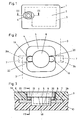
- the 1 shows a data carrier 1, which has a per se known chip module 4, which is embedded in the cavities 5 and 6 shown in Figure 3.
- the attachment of the chip module 4 in the cavities 5 and 6 takes place in a conventional manner, for example with an adhesive.
- the chip module 4 is connected to an antenna 3, which is preferably embedded in a card body 2.
- the antenna 3 is, for example, an etched, printed, wound or laid coil of copper. It is arranged according to FIG. 3 on a lower layer 10 of the card body 2 and this layer 10 is connected to an overlying further layer 9.
- the two layers 9 and 10 are connected to each other, for example, by lamination.
- the body 2 can also have further layers not shown here.
- the layers 9 and 10 are preferably plastic layers, for example made of polycarbonate or PVC.
- the two ends 3a and 3b of the antenna 3 are connected electrically and mechanically according to FIG. 2 with a contact bridge 7.
- the connection is made for example by soldering.
- the contact bridge 7 is inserted according to Figure 3 in the layer 10 and has in a groove-shaped recess 19, a noble metal layer 8.
- the noble metal layer 8 consists, for example and preferably, of gold and is comparatively thin and is applied to a flat surface 11 of the recess 19, as FIG. 4 shows.
- the noble metal layer 8 forms a first contact surface 17.
- the aforementioned two cavities 5 and 6 are arranged so that they are located above the contact bridge 7, wherein a second cavity 6 is made so that it breaks through the contact bridge 7 according to FIG.
- the first cavity 5 is less deep, but wider and extends over the separate noble metal layers 8.
- the chip module 4 inserted in the cavities 5 and 6 is indicated by dashed lines.
- two cutouts 20 are incorporated, which expose the card body 2 on the noble metal layers 8. These cutouts 20 are produced in particular with a suitable milling cutter. For electrical and mechanical connection of the noble metal layers 8 with contact surfaces 18 of the chip module 4, the cutout 20 is filled with a contact paste.
- the connections of the chip module 4 to the antenna 3 thus takes place via this contact paste, the noble metal layers 8 and via the contact bridge 7 and the solder joints at the ends 3a and 3b of the antenna 3.
- the contact surfaces 18 of the chip module 4 can also be formed by noble metal layers, not shown here ,
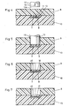
- the method for producing the data carrier 1 will be explained in more detail below.
- the contact bridge 7 Before laminating, the contact bridge 7 is fixed on the layer 10 and electrically and mechanically connected to the antenna 3 at its ends 3a and 3b. The connection takes place for example by soldering. The contact bridge 7 is placed exactly in the position in which later the chip module 4 is mounted.
- the two layers 9 and 10 are connected to one another, for example, by lamination.
- the two cavities 5 and 6 are produced with a suitable tool, for example with a milling cutter.
- the contact bridge 7 is disconnected.
- the two cut-outs 20 are produced according to the figures 4 to 6 with a suitable tool 13.
- the tool 13 is so far immersed according to Figure 4 in the direction of the arrow 14 from above into the layer 9 until a front side 13a of the tool 13 touches a top 12 of the contact bridge 7 barely.
- the noble metal layer 8 is not milled off here.
- This noble metal layer 8 is located in the recess 19 and is thus arranged below the top 12 and protected against erosion. So that the tool 13 can be stopped in time during milling, the tool 13 according to FIG. 5 has a known detection unit 15, which responds to the contact bridge 7 and emits a signal as soon as the tool 13 contacts the contact bridge 7.
- a residue 16 may be present over the noble metal layer 8, which is preferably sucked off.
- the noble metal layer 8 is finally exposed according to FIG.
- Both cutouts 20 are made as explained above. They can be produced simultaneously with two parallel guided tools 13, for example with two milling heads.
- contact paste is applied.
- the contact paste is metered so that it projects beyond the second cavity 6.
- this contact paste is pressed into the cutouts 20 and into the recesses 19 and thereby a permanent connection between the second contact surfaces 18 of the chip module 4 and the first contact surfaces 17 of the contact bridge 7 is produced.
- an adhesive for example a hot-melt adhesive, the chip module 4 is now mechanically fastened in the cavities 5 and 6.
- the contact surfaces are also provided with a noble metal coating.
- the data carrier according to the invention therefore, no oxidation can occur in the connections between the chip module 4 and the antenna 3. A permanent electrical connection over a long service life of, for example, 10 years can be ensured.
Landscapes
- Engineering & Computer Science (AREA)
- Microelectronics & Electronic Packaging (AREA)
- Computer Hardware Design (AREA)
- Physics & Mathematics (AREA)
- General Physics & Mathematics (AREA)
- Theoretical Computer Science (AREA)
- Manufacturing & Machinery (AREA)
- Credit Cards Or The Like (AREA)
- Holo Graphy (AREA)
- Inspection Of Paper Currency And Valuable Securities (AREA)
- Thermal Transfer Or Thermal Recording In General (AREA)
Description
- Die Erfindung betrifft ein Verfahren zur Herstellung von Datenträgern nach dem Oberbegriff des Anspruchs 1. Die Erfindung betrifft zudem einen nach diesem Verfahren hergestellten Datenträger.
- Bei der Herstellung von Chip-Karten wird ein Chipmodul in den Kartenkörper implantiert und dieses wird elektrisch und mechanisch mit einer in der Karte eingebetteten Antenne verbunden. Hiermit können Datenträger mit einer so genannten Dual-Funktion hergestellt werden, bei welcher das implantierte Chipmodul sowohl über eine Kontaktfläche als auch berührungslos über die Antenne ansprechbar ist.
- Der Körper für solche Datenträger bzw. Chip-Karten wird insbesondere durch Laminieren mehreren Schichten hergestellt. Die Antenne ist eine geäzte, gedruckte, gewickelte oder gelegte Spule, die auf einer dieser Schichten angeordnet ist.
- Das Implantieren des Chipmoduls kann bei der Herstellung von Datenträgern mit Dual-Funktion im Wesentlichen gleich erfolgen, wie bei der Herstellung einer üblichen Bankkarte. Hierbei wird eine Rohkarte für das Chipmodul ausgefräst und anschliessend wird das Chipmodul in diese Vertiefung hineingeklebt. Diese Vertiefung wird auch Kavitätsfräsung genannt. Soll ein Datenträger mit Dual-Funktion hergestellt werden, so muss die Antenne elektrisch und mechanisch mit dem Chipmodul verbunden werden. Nach einem Stand der Technik wird die Antenne selbst oder Anschlüsse zur Antenne freigefräst und hierbei wird die Antenne oder die Anschlüsse zur Antenne angefräst. Mit einer elektrisch leitenden Paste wird dann das Chipmodul mit der Antenne elektrisch verbunden. Bei diesem Verfahren besteht die Schwierigkeit, dass die angefräste Antenne bzw. die angefrästen Anschlüsse oxidieren können und die elektrische Leitfähigkeit und damit die Funktionssicherheit gestört oder verhindert werden.
- Im Stand der Technik sind zudem die nachfolgenden Verfahren bekannt geworden, mit denen ein Kontakt einer Chip-Karte hergestellt werden soll.
- Die DE-A-101 22 416 offenbart ein Verfahren zur Herstellung einer Chipkarte mit Spule, wobei eine Verbindung zwischen der Spule und den Anschlussflächen eines integrierten Schaltkreises hergestellt wird. Die Verbindung wird mit einer Metallfolie hergestellt, die freigefräst und auch leicht angefräst wird. Das Anfräsen der Metallfolie kann jedoch eine einwandfreie Kontaktierung beeinträchtigen.
- Die DE 197 28 993 C offenbart ein Verfahren zur Herstellung einer Chip-Karte mit einer eingebetteten Antenne, wobei der Kontakt zwischen dem Chipmodul und der Antenne durch einen elektrisch leitenden Stift hergestellt wird, der so weit in die Chip-Karte eingetrieben wird, dass sein vorderes Ende kraftschlüssig mit der Antenne verbunden wird. Der Stift ist vorzugsweise aus Aluminium hergestellt. Auch hier dürfte die Dauerhaftigkeit aufgrund von Oxidationen begrenzt sein.
- Die WO 99/21131 offenbart ebenfalls ein Verfahren zur Herstellung von Chip-Karten, wobei über eine elektrisch leitfähige Masse wie Leitklebstoff oder dergleichen das Chipmodul mit der Antenne verbunden wird. Diese leitfähige Masse wird mittels einer Dosiereinrichtung auf die zweite Kontaktfläche aufgetragen.
- Die WO 98/08191 befasst sich ebenfalls mit einem Verfahren zur Herstellung einer elektrischen und mechanischen Verbindung in einer Chip-Karte, die Verbindung wird unter Verwendung eines Heiss- und Schmelzklebers hergestellt, wobei eine zusätzliche leitfähige Schicht oder leitfähige Partikel verwendet werden.
- Der Erfindung liegt die Aufgabe zugrunde, ein Verfahren der genannten Art zu schaffen, das die genannten Schwierigkeiten vermeidet und eine dauernde elektrische Verbindung insbesondere zwischen einem Chipmodul und einer Antenne bei hoher Einsatzdauer gewährleistet.
- Die Aufgabe ist bei einem gattungsgemässen Verfahren gemäss Anspruch 1 gelöst. Da die Edelmetallschicht vertieft angeordnet ist, kann diese ohne Beschädigung freigelegt werden. Die Edelmetallschicht kann vergleichsweise dünn sein, da sie beim Abtragen des Kartenkörpers nicht beschädigt, beispielsweise angefräst wird. Da nur geringe Mengen eines Edelmetalls, beispielsweise Gold erforderlich sind, um eine solche Schicht herzustellen, sind die zusätzlichen Kosten für diese Schicht vergleichsweise gering. Da die Kontaktfläche, welche durch die Edelmetallschicht gebildet wird, im Gegensatz zu Kupfer oder anderen Buntmetallen nicht oxidiert, kann die elektrische Leitfähigkeit dieser Kontaktstelle und damit die Funktionssicherheit nicht gestört oder verhindert werden. Mit dem erfindungsgemässen Verfahren kann somit in einem Datenträger und insbesondere in einer Chip-Karte eine Kontaktfläche geschaffen werden, die frei von Oxidation ist und die trotzdem keine wesentlich höheren Kosten verursacht.
- Es ist vorgesehen, dass die Edelmetallschicht auf einer in den Kartenkörper eingebetteten Kontaktbrücke angeordnet ist. Diese Kontaktbrücke ist beispielsweise an einer Antenne angelötet und befindet sich zwischen laminierten Schichten des Kartenkörpers. Die Kontaktbrücke wird so in den Kartenkörper eingebettet, dass sie sich nach der Herstellung der Rohkarte immer auf der gleichen Position der X- und Y-Achse der Karte befindet. Beim Herstellen der Kavität für das Chipmodul kann dann gleichzeitig die genannte Edelmetallschicht freigelegt werden.
- Nach einer Weiterbildung der Erfindung wird die Edelmetallschicht mit einem Fräswerkzeug freigelegt. Vorzugsweise weist das Fräswerkzeug eine detektierende Einheit auf und es wird so gefräst, dass die Edelmetallschicht nicht touchiert wird. Die detektierende Einheit ermöglicht es, das Fräswerkzeug exakt so weit in den Körper einzutauchen, dass der Kontaktkörper und insbesondere die Kontaktbrücke leicht touchiert wird.
- Da die Edelmetallschicht vertieft angeordnet ist, wird diese hierbei nicht angefräst und bleibt somit unverletzt. In der Vertiefung über der Metallschicht vergleichende Reste werden nach einer Weiterbildung der Erfindung abgesaugt.
- Nachfolgend wird die Erfindung anhand der Zeichnung näher erläutert. Es zeigen:
- Figur 1
- schematisch eine Ansicht eines erfindungsgemässen Datenträgers,
- Figur 2
- ein stark vergrösserter Ausschnitt aus der Figur 1,
- Figur 3
- ein Schnitt entlang der Linie III-III der Figur 1 und
- Figuren 4-7
- schematisch einzelne Verfahrensschritte.
- Die Figur 1 zeigt einen Datenträger 1, der ein an sich bekanntes Chipmodul 4 aufweist, welcher in die in Figur 3 gezeigten Kavitäten 5 und 6 eingebettet ist. Die Befestigung des Chipmoduls 4 in die Kavitäten 5 und 6 erfolgt in an sich bekannter Weise beispielsweise mit einem Klebstoff. Das Chipmodul 4 ist mit einer Antenne 3 verbunden, die vorzugsweise in einen Kartenkörper 2 eingebettet ist. Die Antenne 3 ist beispielsweise eine geäzte, gedruckte, gewickelte oder gelegte Spule aus Kupfer. Sie ist gemäss Figur 3 auf einer unteren Schicht 10 des Kartenkörpers 2 angeordnet und diese Schicht 10 ist mit einer darüber liegenden weiteren Schicht 9 verbunden. Die beiden Schichten 9 und 10 sind beispielsweise durch Laminieren miteinander verbunden. Grundsätzlich kann der Körper 2 auch noch weitere hier nicht gezeigte Schichten aufweisen. Die Schichten 9 und 10 sind vorzugsweise Kunststoffschichten, beispielsweise aus Polycarbonat oder PVC.
- Die beiden Enden 3a und 3b der Antenne 3 sind gemäss Figur 2 mit einer Kontaktbrücke 7 elektrisch und mechanisch verbunden. Die Verbindung erfolgt beispielsweise durch Löten. Die Kontaktbrücke 7 ist gemäss Figur 3 in die Schicht 10 eingelegt und weist in einer nutenförmigen Vertiefung 19 eine Edelmetallschicht 8 auf. Die Edelmetallschicht 8 besteht beispielsweise und vorzugsweise aus Gold ist und vergleichsweise dünn und ist auf eine ebene Fläche 11 der Vertiefung 19 aufgetragen, wie die Figur 4 zeigt. Die Edelmetallschicht 8 bildet eine erste Kontaktfläche 17.
- Die genannten beiden Kavitäten 5 und 6 sind so angeordnet, dass diese sich über der Kontaktbrücke 7 befinden, wobei eine zweite Kavität 6 so hergestellt ist, dass sie die Kontaktbrücke 7 gemäss Figur 3 durchbricht. Die erste Kavität 5 ist weniger tief, jedoch breiter und erstreckt sich über die von einander getrennten Edelmetallschichten 8. In der Figur 3 ist gestrichelt das in die Kavitäten 5 und 6 eingelegte Chipmodul 4 angedeutet. In den Kartenkörper 2 sind zwei Ausfräsungen 20 eingearbeitet, welche den Kartenkörper 2 über den Edelmetallschichten 8 freilegen. Diese Ausfräsungen 20 werden insbesondere mit einem geeigneten Fräser hergestellt. Zur elektrischen und mechanischen Verbindung der Edelmetallschichten 8 mit Kontaktflächen 18 des Chipmoduls 4 wird die Ausfräsung 20 mit einer Kontaktpaste ausgefüllt. Die Verbindungen des Chipmoduls 4 zur Antenne 3 erfolgt somit über diese Kontaktpaste, die Edelmetallschichten 8 sowie über die Kontaktbrücke 7 und die Lötstellen an den Enden 3a und 3b der Antenne 3. Die Kontaktflächen 18 des Chipmoduls 4 können ebenfalls durch hier nicht gezeigte Edelmetallschichten gebildet sein.
- Nachfolgend wird das Verfahren zur Herstellung des Datenträgers 1 näher erläutert.
- Vor dem Laminieren wird auf der Schicht 10 die Kontaktbrücke 7 befestigt und mit der Antenne 3 an ihren Enden 3a und 3b elektrisch und mechanisch verbunden. Das Verbinden erfolgt beispielsweise durch Löten. Die Kontaktbrücke 7 wird genau in der Position angeordnet, in welcher später das Chipmodul 4 montiert wird.
- Sind die Kontaktbrücke 7 und die Antenne 3 gelegt, so werden die beiden Schichten 9 und 10 beispielsweise durch Laminieren miteinander verbunden. Nun werden die beiden Kavitäten 5 und 6 mit einem geeigneten Werkzeug, beispielsweise mit einem Fräser hergestellt. Durch die zweite Kavität 6 wird die Kontaktbrücke 7 getrennt. Nun werden die beiden Ausfräsungen 20 gemäss den Figuren 4 bis 6 mit einem geeigneten Werkzeug 13 hergestellt. Das Werkzeug 13 wird gemäss Figur 4 in Richtung des Pfeils 14 von oben in die Schicht 9 so weit eingetaucht, bis eine Frontseite 13a des Werkzeuges 13 eine Oberseite 12 der Kontaktbrücke 7 knapp touchiert. Wesentlich ist nun, dass die Edelmetallschicht 8 hierbei nicht abgefräst wird. Diese Edelmetallschicht 8 befindet sich in der Vertiefung 19 und ist somit unterhalb der Oberseite 12 angeordnet und gegen einen Abtrag geschützt. Damit das Werkzeug 13 beim Fräsen rechtzeitig gestoppt werden kann, weist das Werkzeug 13 gemäss Figur 5 eine an sich bekannte Detektiereinheit 15 auf, welche auf die Kontaktbrücke 7 anspricht und ein Signal abgibt, sobald das Werkzeug 13 die Kontaktbrücke 7 berührt.
- In der Vertiefung 19 kann über der Edelmetallschicht 8 ein Rest 16 vorhanden sein, der vorzugsweise abgesaugt wird. Die Edelmetallschicht 8 ist schliesslich gemäss Figur 7 freigelegt.
- Beide Ausfräsungen 20 werden wie oben erläutert hergestellt. Sie können gleichzeitig mit zwei parallel geführten Werkzeugen 13, beispielsweise mit zwei Fräsköpfen hergestellt werden.
- Auf die freigelegten Edelmetallschichten 8 wird nun eine hier nicht gezeigte Kontaktpaste aufgetragen. Die Kontaktpaste ist so dosiert, dass sie die zweite Kavität 6 überragt. Beim Implantieren des Chipmoduls 4 wird diese Kontaktpaste in die Ausfräsungen 20 und in die Vertiefungen 19 hineingepresst und dadurch wird eine dauernde Verbindung zwischen den zweiten Kontaktflächen 18 des Chipmoduls 4 und den ersten Kontaktflächen 17 der Kontaktbrücke 7 hergestellt. Mit einem Kleber, beispielsweise einem Hot-Melt-Kleber wird nun das Chipmodul 4 mechanisch in den Kavitäten 5 und 6 befestigt.
- Bei den üblichen zur Herstellung von Chip-Karten verwendeten Chipmodulen 4 sind die Kontaktflächen ebenfalls mit einer Edelmetallbeschichtung versehen. Beim erfindungsgemässen Datenträger kann deshalb keine Oxidation bei den Verbindungen zwischen dem Chipmodul 4 und der Antenne 3 entstehen. Eine dauernde elektrische Verbindung über eine hohe Einsatzdauer von beispielsweise 10 Jahren kann dadurch sichergestellt werden.
-
- 1.
- Datenträger
- 2.
- Kartenkörper
- 3.
- Antenne
- 3.a
- Ende
- 3.b
- Ende
- 4.
- Chipmodul
- 5.
- erste Kavität
- 6.
- zweite Kavität
- 7.
- Kontaktbrücke
- 8.
- Edelmetall
- 9.
- Kartenschicht
- 10.
- Kartenschicht
- 11.
- ebene Fläche der Kontaktbrücke
- 12.
- Oberseite der Kontaktbrücke
- 13.
- Werkzeug
- 13.a
- Frontseite
- 14.
- Pfeil
- 15.
- Detektiereinheit
- 16.
- Rest
- 17.
- erste Kontaktfläche
- 18.
- zweite Kontaktfläche
- 19.
- Vertiefung
- 20.
- Ausfräsung
Claims (7)
- Verfahren zur Herstellung von Datenträgern (1), bei denen wenigstens eine erste Kontaktfläche (17) eines ersten Bauteils (3, 7), der eine Antenne (3) und eine mit dieser verbundene Kontaktbrücke (7) aufweist, mit einer zweiten Kontaktfläche (18) eines in einen Körper (2) des Datenträgers (1) eingebetteten zweiten Bauteils (4) elektrisch und mechanisch verbunden wird, die erste Kontaktfläche (17) durch eine vertieft angeordnete und in den Körper (2) eingebettete Edelmetallschicht (8) gebildet wird und dass diese Edelmetallschicht (8) mit einem Werkzeug (13) freigelegt wird, wobei ein Bereich des Körpers (2) über der Edelmetallschicht (8) abgetragen wird und dass die freigelegte Edelmetallschicht (8) mit der zweiten Kontaktfläche (18) elektrisch und mechanisch verbunden wird, dadurch gekennzeichnet, dass die Edelmetallschicht (8) in einer Vertiefung der Kontaktbrücke (7) unterhalb der Oberseite der mit der Antenne verbundenen Kontaktbrücke (7) angeordnet wird, wobei die Edelmetallschicht in folgenden Schritten freigelegt wird:- das Werkzeug entfernt einen Bereich des Kartenkörpers, bis zur genannten Oberseite der Kontaktbrücke (7),- die in der Vertiefung über der Edelmetallschicht verbleibende Resten des Kartenkörpers werden entfernt.
- Verfahren nach Anspruch 1, dadurch gekennzeichnet, dass das Werkzeug mit der genannten Oberseite der Kontaktbrücke (7) in Berührung kommt.
- Verfahren nach Anspruch 1 oder 2, dadurch gekennzeichnet, dass die Edelmetallschicht (8) mit einem Fräswerkzeug (13) freigelegt wird.
- Verfahren nach Anspruch 3, dadurch gekennzeichnet, dass das Fräswerkzeug (13) eine Detektiereinheit (15) aufweist, welche auf die Kontaktbrücke (7) anspricht und ein Signal abgibt, sobald das Werkzeug (13) die Kontaktbrücke berührt.
- Verfahren nach einem der Ansprüche 1 bis 4, dadurch gekennzeichnet, dass die nach dem Abtragen über der Edelmetallschicht (8) verbleibende Resten (16) des Kartenkörpers abgesaugt werden.
- Datenträger hergestellt nach dem Verfahren gemäss Anspruch 1, dadurch gekennzeichnet, dass er eine Chip-Karte ist und dass die Edelmetallschicht in der Vertiefung der Kontaktbrücke (7) ohne Beschädigung ist und dass die Oberseite der Kontaktbrücke über der Vertiefung angefräst ist.
- Datenträger gemäss Anspruch 6, dadurch gekennzeichnet, dass die Edelmetallschicht (8) aus Gold ist.
Priority Applications (8)
| Application Number | Priority Date | Filing Date | Title |
|---|---|---|---|
| EP03405839A EP1536372B1 (de) | 2003-11-25 | 2003-11-25 | Verfahren zur Herstellung von Datenträgern und nach diesem Verfahren hergestellter Datenträger |
| PT03405839T PT1536372E (pt) | 2003-11-25 | 2003-11-25 | Processo para a produção de portadores de dados e portadores de dados produzidos de acordo com este processo |
| AT03405839T ATE335255T1 (de) | 2003-11-25 | 2003-11-25 | Verfahren zur herstellung von datenträgern und nach diesem verfahren hergestellter datenträger |
| DK03405839T DK1536372T3 (da) | 2003-11-25 | 2003-11-25 | Fremgangsmåde til fremstilling af databærere og databærere der er fremstillet ifölge denne fremgangsmåde |
| DE50304499T DE50304499D1 (de) | 2003-11-25 | 2003-11-25 | Verfahren zur Herstellung von Datenträgern und nach diesem Verfahren hergestellter Datenträger |
| ES03405839T ES2269958T3 (es) | 2003-11-25 | 2003-11-25 | Procedimiento de fabricacion de un soporte de datos y el soporte de datos fabricado segun este procedimiento. |
| SI200330508T SI1536372T1 (sl) | 2003-11-25 | 2003-11-25 | Postopek za izdelavo podatkovnih nosilcev in po tem postopku izdelani podatkovni nosilec |
| CY20061101531T CY1106218T1 (el) | 2003-11-25 | 2006-10-24 | Μεθοδος για την κατασκευη φορεων δεδομενων και φορεας δεδομενων κατασκευασμενος με αυτη τη μεθοδο |
Applications Claiming Priority (1)
| Application Number | Priority Date | Filing Date | Title |
|---|---|---|---|
| EP03405839A EP1536372B1 (de) | 2003-11-25 | 2003-11-25 | Verfahren zur Herstellung von Datenträgern und nach diesem Verfahren hergestellter Datenträger |
Publications (2)
| Publication Number | Publication Date |
|---|---|
| EP1536372A1 EP1536372A1 (de) | 2005-06-01 |
| EP1536372B1 true EP1536372B1 (de) | 2006-08-02 |
Family
ID=34443144
Family Applications (1)
| Application Number | Title | Priority Date | Filing Date |
|---|---|---|---|
| EP03405839A Expired - Lifetime EP1536372B1 (de) | 2003-11-25 | 2003-11-25 | Verfahren zur Herstellung von Datenträgern und nach diesem Verfahren hergestellter Datenträger |
Country Status (8)
| Country | Link |
|---|---|
| EP (1) | EP1536372B1 (de) |
| AT (1) | ATE335255T1 (de) |
| CY (1) | CY1106218T1 (de) |
| DE (1) | DE50304499D1 (de) |
| DK (1) | DK1536372T3 (de) |
| ES (1) | ES2269958T3 (de) |
| PT (1) | PT1536372E (de) |
| SI (1) | SI1536372T1 (de) |
Families Citing this family (1)
| Publication number | Priority date | Publication date | Assignee | Title |
|---|---|---|---|---|
| WO2017149426A1 (en) * | 2016-02-29 | 2017-09-08 | Thin Film Electronics Asa | Electronic device and method of making the same using surface mount technology and an anisotropic conductive adhesive useful in the method |
Family Cites Families (5)
| Publication number | Priority date | Publication date | Assignee | Title |
|---|---|---|---|---|
| DE19505245C1 (de) * | 1995-02-16 | 1996-04-25 | Karl Heinz Wendisch | Ausweischipkarte mit Antennenwicklung |
| DE19645083C2 (de) * | 1996-11-01 | 2000-01-27 | Austria Card Gmbh Wien | Kontaktlose Chipkarte mit Transponderspule |
| DE19720226C5 (de) * | 1997-05-14 | 2007-11-22 | Künnecke Verwaltungs GmbH & Co. Holding KG | Verfahren und Vorrichtung zur Herstellung von Chipkarten |
| FR2798873B1 (fr) * | 1999-09-28 | 2005-03-11 | Cybernetix | Procede et dispositif d'usinage d'objets integrant un element electriquement conducteur |
| DE10122416A1 (de) * | 2001-05-09 | 2002-11-14 | Giesecke & Devrient Gmbh | Verfahren und Halbzeug zur Herstellung einer Chipkarte mit Spule |
-
2003
- 2003-11-25 SI SI200330508T patent/SI1536372T1/sl unknown
- 2003-11-25 PT PT03405839T patent/PT1536372E/pt unknown
- 2003-11-25 EP EP03405839A patent/EP1536372B1/de not_active Expired - Lifetime
- 2003-11-25 DE DE50304499T patent/DE50304499D1/de not_active Expired - Lifetime
- 2003-11-25 DK DK03405839T patent/DK1536372T3/da active
- 2003-11-25 AT AT03405839T patent/ATE335255T1/de not_active IP Right Cessation
- 2003-11-25 ES ES03405839T patent/ES2269958T3/es not_active Expired - Lifetime
-
2006
- 2006-10-24 CY CY20061101531T patent/CY1106218T1/el unknown
Also Published As
| Publication number | Publication date |
|---|---|
| DK1536372T3 (da) | 2006-11-27 |
| DE50304499D1 (de) | 2006-09-14 |
| EP1536372A1 (de) | 2005-06-01 |
| ES2269958T3 (es) | 2007-04-01 |
| PT1536372E (pt) | 2006-12-29 |
| CY1106218T1 (el) | 2011-06-08 |
| SI1536372T1 (sl) | 2007-02-28 |
| ATE335255T1 (de) | 2006-08-15 |
Similar Documents
| Publication | Publication Date | Title |
|---|---|---|
| DE19500925C2 (de) | Verfahren zur Herstellung einer kontaktlosen Chipkarte | |
| EP0869453B1 (de) | Verfahren zur Herstellung einer Chipkarte | |
| EP1162569B1 (de) | Verfahren zur Herstellung eines Datenträgers | |
| EP0902973B1 (de) | Trägerelement für einen halbleiterchip | |
| DE19651566A1 (de) | Chip-Modul sowie Verfahren zu dessen Herstellung | |
| EP1269410B1 (de) | Verfahren zur herstellung eines trägerbandes mit einer vielzahl von elektrischen einheiten, jeweils aufweisend einen chip und kontaktelemente | |
| EP3599636B1 (de) | Keramischer schaltungsträger und elektronikeinheit | |
| DE3424241A1 (de) | Automatisiertes herstellungsverfahren fuer eine gedruckte schaltung bzw. leiterplatte und deren anwendungsbereich | |
| DE19741984B4 (de) | Chipträger zur Herstellung einer Chipkarte sowie Verfahren zur Herstellung einer derartigen Chipkarte | |
| DE202007013680U1 (de) | Vorrichtung zur Herstellung einer Chipkarte | |
| DE60128537T2 (de) | Zusammenbau zur verbindung von mindestens zwei gedruckten schaltungen | |
| DE19610044C2 (de) | Kartenkörper und Verfahren zur Herstellung einer Chipkarte | |
| EP1536372B1 (de) | Verfahren zur Herstellung von Datenträgern und nach diesem Verfahren hergestellter Datenträger | |
| WO2008138531A1 (de) | Kontaktloses übertragungssystem und verfahren zum herstellen desselben | |
| WO1999006948A1 (de) | Verfahren zur herstellung einer chipkarte für kontaktlose daten- und/oder energieübertragung sowie chipkarte | |
| DE102011085471A1 (de) | Anordnung zur Direktkontaktierung von Kontaktmitteln und zugehörige Anschlusseinheit für eine Druckmesszelle | |
| EP1520253B1 (de) | Verfahren zur herstellung von elektrisch leitfähigen verbindungen auf chipkarten | |
| WO1998039732A2 (de) | Chipkartenmodul und diesen umfassende chipkarte | |
| DE102005002732A1 (de) | Tragbarer Datenträger | |
| DE102007030650B4 (de) | Verfahren zur Herstellung einer Chipkarte | |
| DE3046192C2 (de) | ||
| DE19632814A1 (de) | Kombikarte und Verfahren zu ihrer Herstellung | |
| DE19609134A1 (de) | Verfahren zur Herstellung eines Datenträgers mit einem elektronischen Modul | |
| DE102018201326B4 (de) | Kontaktanordnung, elektronisches Leistungsmodul und Verfahren zur Herstellung eines elektronischen Leistungsmoduls | |
| DE10025147C2 (de) | Kontaktanordnung für mehrkomponentige Smart Cards |
Legal Events
| Date | Code | Title | Description |
|---|---|---|---|
| PUAI | Public reference made under article 153(3) epc to a published international application that has entered the european phase |
Free format text: ORIGINAL CODE: 0009012 |
|
| AK | Designated contracting states |
Kind code of ref document: A1 Designated state(s): AT BE BG CH CY CZ DE DK EE ES FI FR GB GR HU IE IT LI LU MC NL PT RO SE SI SK TR |
|
| AX | Request for extension of the european patent |
Extension state: AL LT LV MK |
|
| 17P | Request for examination filed |
Effective date: 20050728 |
|
| AKX | Designation fees paid |
Designated state(s): AT BE BG CH CY CZ DE DK EE ES FI FR GB GR HU IE IT LI LU MC NL PT RO SE SI SK TR |
|
| AXX | Extension fees paid |
Extension state: LV Payment date: 20050728 Extension state: LT Payment date: 20050728 Extension state: MK Payment date: 20050728 Extension state: AL Payment date: 20050728 |
|
| GRAP | Despatch of communication of intention to grant a patent |
Free format text: ORIGINAL CODE: EPIDOSNIGR1 |
|
| GRAS | Grant fee paid |
Free format text: ORIGINAL CODE: EPIDOSNIGR3 |
|
| GRAA | (expected) grant |
Free format text: ORIGINAL CODE: 0009210 |
|
| AK | Designated contracting states |
Kind code of ref document: B1 Designated state(s): AT BE BG CH CY CZ DE DK EE ES FI FR GB GR HU IE IT LI LU MC NL PT RO SE SI SK TR |
|
| AX | Request for extension of the european patent |
Extension state: AL LT LV MK |
|
| PG25 | Lapsed in a contracting state [announced via postgrant information from national office to epo] |
Ref country code: IT Free format text: LAPSE BECAUSE OF FAILURE TO SUBMIT A TRANSLATION OF THE DESCRIPTION OR TO PAY THE FEE WITHIN THE PRESCRIBED TIME-LIMIT;WARNING: LAPSES OF ITALIAN PATENTS WITH EFFECTIVE DATE BEFORE 2007 MAY HAVE OCCURRED AT ANY TIME BEFORE 2007. THE CORRECT EFFECTIVE DATE MAY BE DIFFERENT FROM THE ONE RECORDED. Effective date: 20060802 |
|
| REG | Reference to a national code |
Ref country code: GB Ref legal event code: FG4D Free format text: NOT ENGLISH |
|
| REG | Reference to a national code |
Ref country code: CH Ref legal event code: EP |
|
| REG | Reference to a national code |
Ref country code: IE Ref legal event code: FG4D Free format text: LANGUAGE OF EP DOCUMENT: GERMAN |
|
| REF | Corresponds to: |
Ref document number: 50304499 Country of ref document: DE Date of ref document: 20060914 Kind code of ref document: P |
|
| REG | Reference to a national code |
Ref country code: CH Ref legal event code: NV Representative=s name: ISLER & PEDRAZZINI AG |
|
| REG | Reference to a national code |
Ref country code: RO Ref legal event code: EPE |
|
| GBT | Gb: translation of ep patent filed (gb section 77(6)(a)/1977) |
Effective date: 20061017 |
|
| REG | Reference to a national code |
Ref country code: SE Ref legal event code: TRGR |
|
| REG | Reference to a national code |
Ref country code: GR Ref legal event code: EP Ref document number: 20060403662 Country of ref document: GR |
|
| REG | Reference to a national code |
Ref country code: DK Ref legal event code: T3 |
|
| REG | Reference to a national code |
Ref country code: EE Ref legal event code: FG4A Ref document number: E000704 Country of ref document: EE Effective date: 20061005 |
|
| REG | Reference to a national code |
Ref country code: PT Ref legal event code: SC4A Free format text: AVAILABILITY OF NATIONAL TRANSLATION Effective date: 20061019 |
|
| REG | Reference to a national code |
Ref country code: HU Ref legal event code: AG4A Ref document number: E000879 Country of ref document: HU |
|
| ET | Fr: translation filed | ||
| REG | Reference to a national code |
Ref country code: ES Ref legal event code: FG2A Ref document number: 2269958 Country of ref document: ES Kind code of ref document: T3 |
|
| PLBE | No opposition filed within time limit |
Free format text: ORIGINAL CODE: 0009261 |
|
| STAA | Information on the status of an ep patent application or granted ep patent |
Free format text: STATUS: NO OPPOSITION FILED WITHIN TIME LIMIT |
|
| 26N | No opposition filed |
Effective date: 20070503 |
|
| REG | Reference to a national code |
Ref country code: CH Ref legal event code: PCAR Free format text: ISLER & PEDRAZZINI AG;POSTFACH 1772;8027 ZUERICH (CH) |
|
| PGFP | Annual fee paid to national office [announced via postgrant information from national office to epo] |
Ref country code: CZ Payment date: 20081029 Year of fee payment: 6 Ref country code: DK Payment date: 20081015 Year of fee payment: 6 Ref country code: EE Payment date: 20081027 Year of fee payment: 6 Ref country code: IE Payment date: 20081016 Year of fee payment: 6 Ref country code: LU Payment date: 20081021 Year of fee payment: 6 Ref country code: MC Payment date: 20081022 Year of fee payment: 6 Ref country code: NL Payment date: 20081017 Year of fee payment: 6 Ref country code: TR Payment date: 20081021 Year of fee payment: 6 |
|
| PGFP | Annual fee paid to national office [announced via postgrant information from national office to epo] |
Ref country code: AT Payment date: 20081009 Year of fee payment: 6 Ref country code: ES Payment date: 20081111 Year of fee payment: 6 Ref country code: FI Payment date: 20081016 Year of fee payment: 6 Ref country code: PT Payment date: 20081020 Year of fee payment: 6 Ref country code: RO Payment date: 20081104 Year of fee payment: 6 Ref country code: SK Payment date: 20081031 Year of fee payment: 6 |
|
| PGFP | Annual fee paid to national office [announced via postgrant information from national office to epo] |
Ref country code: CY Payment date: 20081021 Year of fee payment: 6 Ref country code: SE Payment date: 20081020 Year of fee payment: 6 Ref country code: BG Payment date: 20081030 Year of fee payment: 6 Ref country code: IT Payment date: 20081020 Year of fee payment: 6 Ref country code: BE Payment date: 20081128 Year of fee payment: 6 |
|
| PGFP | Annual fee paid to national office [announced via postgrant information from national office to epo] |
Ref country code: FR Payment date: 20081013 Year of fee payment: 6 |
|
| PGFP | Annual fee paid to national office [announced via postgrant information from national office to epo] |
Ref country code: GB Payment date: 20081022 Year of fee payment: 6 Ref country code: GR Payment date: 20081017 Year of fee payment: 6 Ref country code: SI Payment date: 20081024 Year of fee payment: 6 |
|
| PGFP | Annual fee paid to national office [announced via postgrant information from national office to epo] |
Ref country code: HU Payment date: 20081030 Year of fee payment: 6 |
|
| BERE | Be: lapsed |
Owner name: *TRUB A.G. Effective date: 20091130 |
|
| REG | Reference to a national code |
Ref country code: PT Ref legal event code: MM4A Free format text: LAPSE DUE TO NON-PAYMENT OF FEES Effective date: 20100525 |
|
| REG | Reference to a national code |
Ref country code: NL Ref legal event code: V1 Effective date: 20100601 |
|
| EUG | Se: european patent has lapsed | ||
| PG25 | Lapsed in a contracting state [announced via postgrant information from national office to epo] |
Ref country code: MC Free format text: LAPSE BECAUSE OF NON-PAYMENT OF DUE FEES Effective date: 20091130 |
|
| REG | Reference to a national code |
Ref country code: DK Ref legal event code: EBP |
|
| GBPC | Gb: european patent ceased through non-payment of renewal fee |
Effective date: 20091125 |
|
| PG25 | Lapsed in a contracting state [announced via postgrant information from national office to epo] |
Ref country code: EE Free format text: LAPSE BECAUSE OF NON-PAYMENT OF DUE FEES Effective date: 20091130 Ref country code: BG Free format text: FAILURE TO ELECT DOMICILE IN THE NATIONAL COUNTRY Effective date: 20100531 Ref country code: PT Free format text: LAPSE BECAUSE OF NON-PAYMENT OF DUE FEES Effective date: 20100525 Ref country code: HU Free format text: LAPSE BECAUSE OF NON-PAYMENT OF DUE FEES Effective date: 20091126 |
|
| REG | Reference to a national code |
Ref country code: SK Ref legal event code: MM4A Ref document number: E 1149 Country of ref document: SK Effective date: 20091125 |
|
| REG | Reference to a national code |
Ref country code: EE Ref legal event code: MM4A Ref document number: E000704 Country of ref document: EE Effective date: 20091130 |
|
| REG | Reference to a national code |
Ref country code: FR Ref legal event code: ST Effective date: 20100730 |
|
| PG25 | Lapsed in a contracting state [announced via postgrant information from national office to epo] |
Ref country code: CZ Free format text: LAPSE BECAUSE OF NON-PAYMENT OF DUE FEES Effective date: 20091125 Ref country code: SK Free format text: LAPSE BECAUSE OF NON-PAYMENT OF DUE FEES Effective date: 20091125 Ref country code: FI Free format text: LAPSE BECAUSE OF NON-PAYMENT OF DUE FEES Effective date: 20091125 Ref country code: AT Free format text: LAPSE BECAUSE OF NON-PAYMENT OF DUE FEES Effective date: 20091125 |
|
| REG | Reference to a national code |
Ref country code: SI Ref legal event code: KO00 Effective date: 20100823 |
|
| PG25 | Lapsed in a contracting state [announced via postgrant information from national office to epo] |
Ref country code: GR Free format text: LAPSE BECAUSE OF NON-PAYMENT OF DUE FEES Effective date: 20100602 Ref country code: IE Free format text: LAPSE BECAUSE OF NON-PAYMENT OF DUE FEES Effective date: 20091125 Ref country code: NL Free format text: LAPSE BECAUSE OF NON-PAYMENT OF DUE FEES Effective date: 20100601 Ref country code: FR Free format text: LAPSE BECAUSE OF NON-PAYMENT OF DUE FEES Effective date: 20091130 Ref country code: CY Free format text: LAPSE BECAUSE OF NON-PAYMENT OF DUE FEES Effective date: 20091125 Ref country code: BE Free format text: LAPSE BECAUSE OF NON-PAYMENT OF DUE FEES Effective date: 20091130 |
|
| PG25 | Lapsed in a contracting state [announced via postgrant information from national office to epo] |
Ref country code: SI Free format text: LAPSE BECAUSE OF NON-PAYMENT OF DUE FEES Effective date: 20091126 |
|
| PG25 | Lapsed in a contracting state [announced via postgrant information from national office to epo] |
Ref country code: GB Free format text: LAPSE BECAUSE OF NON-PAYMENT OF DUE FEES Effective date: 20091125 |
|
| PG25 | Lapsed in a contracting state [announced via postgrant information from national office to epo] |
Ref country code: DK Free format text: LAPSE BECAUSE OF NON-PAYMENT OF DUE FEES Effective date: 20091130 |
|
| PG25 | Lapsed in a contracting state [announced via postgrant information from national office to epo] |
Ref country code: RO Free format text: LAPSE BECAUSE OF NON-PAYMENT OF DUE FEES Effective date: 20091125 |
|
| REG | Reference to a national code |
Ref country code: ES Ref legal event code: FD2A Effective date: 20110329 |
|
| PG25 | Lapsed in a contracting state [announced via postgrant information from national office to epo] |
Ref country code: IT Free format text: LAPSE BECAUSE OF NON-PAYMENT OF DUE FEES Effective date: 20091125 |
|
| PG25 | Lapsed in a contracting state [announced via postgrant information from national office to epo] |
Ref country code: LU Free format text: LAPSE BECAUSE OF NON-PAYMENT OF DUE FEES Effective date: 20091125 |
|
| PG25 | Lapsed in a contracting state [announced via postgrant information from national office to epo] |
Ref country code: SE Free format text: LAPSE BECAUSE OF NON-PAYMENT OF DUE FEES Effective date: 20091126 |
|
| PG25 | Lapsed in a contracting state [announced via postgrant information from national office to epo] |
Ref country code: ES Free format text: LAPSE BECAUSE OF NON-PAYMENT OF DUE FEES Effective date: 20110316 |
|
| PG25 | Lapsed in a contracting state [announced via postgrant information from national office to epo] |
Ref country code: ES Free format text: LAPSE BECAUSE OF NON-PAYMENT OF DUE FEES Effective date: 20091126 |
|
| PG25 | Lapsed in a contracting state [announced via postgrant information from national office to epo] |
Ref country code: TR Free format text: LAPSE BECAUSE OF NON-PAYMENT OF DUE FEES Effective date: 20091125 |
|
| REG | Reference to a national code |
Ref country code: CH Ref legal event code: PUE Owner name: GEMALTO AG, CH Free format text: FORMER OWNER: TRUEB AG, CH |
|
| REG | Reference to a national code |
Ref country code: DE Ref legal event code: R082 Ref document number: 50304499 Country of ref document: DE Representative=s name: HEINRICH ERB PARTNER RECHTSANWAELTE PATENTANWA, DE Ref country code: DE Ref legal event code: R081 Ref document number: 50304499 Country of ref document: DE Owner name: GEMALTO AG, CH Free format text: FORMER OWNER: TRUEB AG, AARAU, CH Ref country code: DE Ref legal event code: R082 Ref document number: 50304499 Country of ref document: DE Representative=s name: PATENTANWAELTE OLBRICHT, BUCHHOLD, KEULERTZ PA, DE |
|
| REG | Reference to a national code |
Ref country code: DE Ref legal event code: R082 Ref document number: 50304499 Country of ref document: DE Representative=s name: PATENTANWAELTE OLBRICHT, BUCHHOLD, KEULERTZ PA, DE |
|
| PGFP | Annual fee paid to national office [announced via postgrant information from national office to epo] |
Ref country code: DE Payment date: 20221020 Year of fee payment: 20 |
|
| PGFP | Annual fee paid to national office [announced via postgrant information from national office to epo] |
Ref country code: CH Payment date: 20221201 Year of fee payment: 20 |
|
| P01 | Opt-out of the competence of the unified patent court (upc) registered |
Effective date: 20230502 |
|
| REG | Reference to a national code |
Ref country code: DE Ref legal event code: R071 Ref document number: 50304499 Country of ref document: DE |
|
| REG | Reference to a national code |
Ref country code: CH Ref legal event code: PL |