EP1535803A1 - Zentralelektrik für ein Kraftfahrzeug - Google Patents
Zentralelektrik für ein Kraftfahrzeug Download PDFInfo
- Publication number
- EP1535803A1 EP1535803A1 EP03027508A EP03027508A EP1535803A1 EP 1535803 A1 EP1535803 A1 EP 1535803A1 EP 03027508 A EP03027508 A EP 03027508A EP 03027508 A EP03027508 A EP 03027508A EP 1535803 A1 EP1535803 A1 EP 1535803A1
- Authority
- EP
- European Patent Office
- Prior art keywords
- busbar
- control circuit
- central electrics
- central
- contact elements
- Prior art date
- Legal status (The legal status is an assumption and is not a legal conclusion. Google has not performed a legal analysis and makes no representation as to the accuracy of the status listed.)
- Granted
Links
- 230000000284 resting effect Effects 0.000 claims abstract description 5
- 238000004519 manufacturing process Methods 0.000 claims description 5
- 210000002105 tongue Anatomy 0.000 description 7
- 238000012546 transfer Methods 0.000 description 7
- 230000017525 heat dissipation Effects 0.000 description 5
- 239000004020 conductor Substances 0.000 description 4
- 239000000758 substrate Substances 0.000 description 4
- 239000000853 adhesive Substances 0.000 description 3
- 230000001070 adhesive effect Effects 0.000 description 3
- 230000000295 complement effect Effects 0.000 description 3
- 239000002184 metal Substances 0.000 description 3
- 230000005855 radiation Effects 0.000 description 3
- 230000008878 coupling Effects 0.000 description 2
- 238000010168 coupling process Methods 0.000 description 2
- 238000005859 coupling reaction Methods 0.000 description 2
- 238000013461 design Methods 0.000 description 2
- 239000003292 glue Substances 0.000 description 2
- 238000002347 injection Methods 0.000 description 2
- 239000007924 injection Substances 0.000 description 2
- 238000003780 insertion Methods 0.000 description 2
- 230000037431 insertion Effects 0.000 description 2
- 238000005259 measurement Methods 0.000 description 2
- 238000000926 separation method Methods 0.000 description 2
- 230000005540 biological transmission Effects 0.000 description 1
- 238000010276 construction Methods 0.000 description 1
- 238000001816 cooling Methods 0.000 description 1
- 238000001514 detection method Methods 0.000 description 1
- 238000011161 development Methods 0.000 description 1
- 230000018109 developmental process Effects 0.000 description 1
- 230000002349 favourable effect Effects 0.000 description 1
- 238000001746 injection moulding Methods 0.000 description 1
- 230000013011 mating Effects 0.000 description 1
- 238000012986 modification Methods 0.000 description 1
- 230000004048 modification Effects 0.000 description 1
- 238000013021 overheating Methods 0.000 description 1
- 238000012545 processing Methods 0.000 description 1
- 230000004044 response Effects 0.000 description 1
- 239000002918 waste heat Substances 0.000 description 1
Images


Classifications
-
- B—PERFORMING OPERATIONS; TRANSPORTING
- B60—VEHICLES IN GENERAL
- B60R—VEHICLES, VEHICLE FITTINGS, OR VEHICLE PARTS, NOT OTHERWISE PROVIDED FOR
- B60R16/00—Electric or fluid circuits specially adapted for vehicles and not otherwise provided for; Arrangement of elements of electric or fluid circuits specially adapted for vehicles and not otherwise provided for
- B60R16/02—Electric or fluid circuits specially adapted for vehicles and not otherwise provided for; Arrangement of elements of electric or fluid circuits specially adapted for vehicles and not otherwise provided for electric constitutive elements
- B60R16/023—Electric or fluid circuits specially adapted for vehicles and not otherwise provided for; Arrangement of elements of electric or fluid circuits specially adapted for vehicles and not otherwise provided for electric constitutive elements for transmission of signals between vehicle parts or subsystems
- B60R16/0238—Electrical distribution centers
Definitions
- the present invention relates to a central electrical system for a motor vehicle.
- Motor vehicles have a plurality of electrical consumers or Loads on, or their supply lines by fuses overload must be secured and / or turned on and off have to.
- a central electrical system is often provided, the over a control circuit and a plurality of load switching devices, for example Relay, and possibly has fuses.
- the control device serves to be fed to her via appropriate control inputs Signals out, the load switching devices to operate and thus appropriate Load circuits to open or close.
- the load switches used in this case serve as a rule for switching relatively large currents, so that they cause considerable waste heat, which may affect the function of the control circuit.
- a good Thermal behavior of the central electrics is therefore for their lifetime of some importance.
- the present invention is therefore based on the object, a central electrics with a simple design that provides a good thermal Behavior shows.
- the central electrical system according to the invention for a motor vehicle comprises a Control circuit on a circuit carrier, at least one busbar, at least partially arranged next to the circuit carrier is and at least one not on the circuit carrier or a part the control circuits resting contact portion, at least two output contact elements on one of the control circuit technological side of the busbar are arranged, and at least two load switching devices, each one with a corresponding Control output of the control circuit electrically connected Control input and two load current connections, one of which with the Power rail and the other, each with one of the two output contact elements electrically connected, have, and the whole or partly on the busbar and / or on one of the control circuits remote from the busbar are arranged.
- a load switching device Under a load switching device is doing any device with two load current terminals, i. a load current input and a Load current output, understood by means of which at least one corresponding Control signal of the control circuit out the respective load current connections, i.e. the respective load current input and the respective load current output, electrically connectable to each other or each other electrically are separable, with larger currents, such as those at certain consumers in motor vehicles, are switched can.
- the busbar is so relative to the circuit carrier arranged at least partially adjacent to the circuit carrier is arranged and at least one not on the circuit board or has a contact portion resting on a part of the control circuit, with which the corresponding load current connections, i. the load current inputs, the load switching devices are connected.
- the busbar does not lie completely on the circuit carrier or the control circuit but extends at least partially alongside and / or under or on the circuit carrier.
- the load switching devices are typically over Contacts connected to the power rail, via the large electrical Currents are feasible and therefore a correspondingly large thermal Have conductivity. Therefore, heat from the load switching devices may continue be discharged directly over the busbar, so that therefore also a lower thermal load of the control circuit and a good cooling of the load switching devices is achieved.
- the circuit carrier, the busbar and the output contact elements on a flat carrier element are arranged, and that a portion of the surface of the support element, on which the output contact elements are arranged, by at least the contact portion of the busbar spatially from the circuit carrier is disconnected.
- at least some of the load switching devices may be arranged.
- the circuit carrier not necessarily in direct contact with the surface of the To be carrier element. Rather, it is possible that this only in small Sections on the busbar rests. Particularly preferred may the busbar in the carrier element or corresponding recesses be pressed into it. Alternatively, it is particularly preferred that Produce carrier element by injection molding and doing the busbar in this at least partially inject.
- the busbar for dissipation heat is thermally coupled to a heat sink.
- the Heat sink is preferably arranged in the central electrical system, that this is not directly in contact with the control circuit or the Circuit carrier of the control circuit is. It is particularly preferred that between the busbar and the heat sink as possible thin layer of a good heat-conducting paste or a good heat-conducting Glue is arranged to ensure the best possible heat transfer between the busbar and the heat sink. Otherwise prevents the then between the busbar and the surface the heat sink unavoidable air gap a good heat transfer.
- a heat sink which is made of an electrically conductive material, In particular, a metal is made, while the thermal takes place Coupling between the busbar and the heat sink preferably by an electrically insulating layer of high thermal conductivity.
- an electrically insulating layer of high thermal conductivity therefor For example, highly thermally conductive, but electrically insulating Glue be used.
- At least one of the load switching devices is held on the busbar.
- the load switching device is at least with an area on the power rail, so that too over the lying surface a particularly good thermal coupling done can.
- load switching devices such as electronic Components that are arranged for example in a housing can.
- At least one load switching device an unpackaged electronic component, preferably a MOSFET device comprising, on the power rail or on a punched grid element is arranged next to the busbar.
- a MOSFET device comprising, on the power rail or on a punched grid element
- the MOSFET device can be arranged on the Busbar used in a so-called "high side” circuit be in which the load switching device between a positive pole of a Power supply and the consumer is switched while at Arrangement on the lead frame a "low side” circuit of the MOSFET device is possible, in which the load switching device with the Negative pole is connected.
- the MOSFET device is also held on the busbar or the punched grid element.
- This will be preferably a highly thermally conductive adhesive is used, which then simultaneously for a particularly good heat transfer between the component and the busbar or the lead frame element leads.
- the control circuit for using a MOSFET device is designed with current measurement.
- a MOSFET device with current measurement or detection is doing a MOSFET device, which is often referred to as a "current sense” output has designated output via which a current signal can be emitted that is the size of the current flowing in the MOSFET device Load current between "source” and “drain” reflects.
- the load switching devices need however, not necessarily to be MOSFET devices. Rather, it is for a modular concept for the production of central electrics with different ones Load switching devices preferred that a control circuit is provided for driving various load switching devices.
- At least one of Load switching devices is a relay that is on the circuit carrier remote from the busbar is arranged.
- this can this be arranged in the region of the surface of the support element, on which the output contact elements are arranged.
- both Busbars do not have at least one the circuit carrier or a part of the control circuit resting Contact section on.
- the load switching devices are whole or partially on the busbars and / or on each of the Control circuit facing away from the busbars arranged. It in this case also results despite a high density of functions or load switching devices a good thermal behavior of the Central electrics.
- either both busbars are thermally with coupled to a heat sink, or it is for each of the busbars provided corresponding heatsink.
- a thermal connection can be produced in the aforementioned manner.
- the output contact elements are designed as plug contact elements. Preferably These may be formed as pins or tongues.
- a housing part with an opening and at least partially surrounding the opening Guidance is provided, and that at least some of the output contact elements are arranged so that these together with the guide form a connector or a device receptacle.
- At least one of the output contact elements in one piece is designed as a bent part, which is not for the production of a plug-in contact used end with the corresponding load current connection one of the load switching devices is connected.
- the load current output At the load power connection So it is the load current output.
- the output contact elements as Stamped sheet metal parts may be formed, which further simplifies the production.
- the circuit carrier with the control circuit connected connector is arranged on the circuit carrier with the control circuit connected connector.
- a connector can be designed in particular as a device holder. Is the circuit carrier formed flat, the plugging direction is preferably aligned orthogonal to the surface of the circuit substrate.
- a fastening device provided is to hold an extension of the power rail and this electrically conductive to connect to the power rail.
- this Power rail can then be another circuit carrier with a control circuit be arranged, which also with at most a small Section of the bus bar is in contact, so that at least contact surfaces the busbar remain free.
- the fastening device is designed to extend two on opposite Sides of the control circuit, preferably arranged in parallel To hold busbars and electrically conductive with the Connect busbars.
- an additional control circuit in turn arranged between the two busbars so that also these spatially from on the extensions of the Busbars arranged load switching devices separated and thus is protected from overheating.
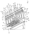
- Fig. 1 and Fig. 2 comprises a central electrical system according to a first preferred Embodiment of the invention in a through a lower housing part 10 and housing 14 formed by a housing upper part 14 as Carrier element, a support plate 16, the two mutually parallel Busbars 18, between the busbars 18 a circuit carrier 20 in the form of a circuit board with a control circuit 22, output contact elements 24, input contact elements 26 and load switching devices in the form of unpackaged or unpacked MOSFET devices 28 carries. Furthermore, in the lower housing part 10 heatsink arranged, of which only the heat sink 30 is shown.
- the support plate 16 is made as an injection molded part made of plastic, wherein in its production, the mutually parallel busbars 18 were partially encapsulated.
- the busbars 18 are mirror-symmetrical to each other and arranged and have on their the circuit carrier 20 opposite, outside teeth with teeth 32 on.
- connecting lugs 34 are formed, only one of which is visible in the figure and that for connection from corresponding cables to a voltage source, for example serve a motor vehicle battery.
- the busbars 18 themselves are off made of a very conductive metal and have a cross section, which allows it to lead over these great streams without great losses.
- the mutually parallel busbars 18 divide the area the support plate 16 in two approximately equal side portions 36 and a middle section 38.
- a connector 42 is arranged, the plugging direction is approximately orthogonal to the surface of the carrier plate 16 runs.
- This connector 42 is used for connection with a complementary connector from a central control device, by means of which the central electrics can be controlled, and points in the Figures not shown connecting lines to the only very schematic shown control circuit 22, so that this corresponding control signals can be supplied.
- In recesses 44 and 46 in the side portions 36 of the support plate 16 are integrally formed as a stamped and bent parts punched grid Output and input contact elements 24 and 26 pressed. These have at their respective the busbars 18 opposite ends orthogonal from the surface of the support plate 16 bent contact contact tongues 48 and 50, respectively (see Fig. 2).
- Each pointing to the busbar 18, as load current inputs Serving load power connections are not visible in the figures, while on the opposite sides of the MOSFET devices 28 arranged with load current outputs serving as load current outputs designated by reference numeral 52.
- the power rails 18 facing load current connections are with contacted directly while serving as load current outputs Load current terminals 52 with the corresponding output contact elements 24 by connecting wires designed for higher currents 54 are connected, of the sake of clarity in the figures not all are shown.
- the MOSFET devices 28 further have control inputs 56, via the MOSFET components 28 each switching signals fed are, in the direction of the load current connections of the respective MOSFET device conductively connected to each other or electrically from each other be disconnected so that the MOSFET devices 28 as electrically can serve actuated switch.
- the control inputs 56 are with Control outputs 58 of the control circuit 22 connected via bonding wires 60, of those in the figures for the sake of clarity only some are shown.
- MOSFET devices 28 have a "currentsense" function, the current signal outputs not shown in the figures the respective MOSFET devices 28 output current signals, which reflect the strength of the load current through these components.
- the Control circuit 22 is for processing these signals for diagnostic purposes educated.
- the non-packaged MOSFET devices 28 on the Teeth 32 of the bus bars 18 are arranged mechanically on the To keep busbars 18, and on the other hand, a good heat transfer between the MOSFET devices 28 and the bus bars 18th These are made with a highly thermally conductive, but electrically insulating adhesive glued to the bus bars 18.
- the input contact elements 26 engage with their busbars 18th facing ends in the spaces between the teeth 32 and are via connection lines 62 with control inputs 64 of the control circuit 22 connected. Of these connecting lines 62 are the For clarity, only a few are shown in the figures.
- the lower housing part 10 is formed as a plastic injection molded part so that it in the frame-like downwardly opening support plate 16 with the arranged components are positively received can.
- the heat sinks are using highly thermally conductive, electrically insulating adhesive with the undersides of the bus bars 18 to form a very good thermal contact associated with only a low thermal resistance.
- the housing upper part 12 has, on the one hand, a connector opening 66 for receiving the connector 42 on the circuit carrier 20 and on the other on opposite sides guide collar 68 and Contact element openings 70, through which the plug contact tongues 48th or 50 of the input and output contact elements 26 and 24 feasible are.
- These guide collar 68 form together with the plug contact tongues 48 or 50 plug connectors in the form of a device receptacle to which Connectors from cables to consumers or loads of the vehicle electrical system can be connected.
- the upper housing part 12, the support plate 16 and the lower housing part 10 are to form the housing via mutually complementary locking elements 72, 73, 74 and 75 locked together.
- the bus bars 18 When installed, the bus bars 18 with a positive pole connected to a motor vehicle battery not shown in the figures. to Supply of signals from central control devices is the Connector 42 on the circuit board 20. Over the through the input and output contact elements 26 and 24 and the guide collar 68 formed device recordings is the central electrical system with appropriate Connected to consumers.
- control circuit 22 In response to control signals, the control circuit 22 outputs corresponding switching signals to one or more of the load switching devices or one or several of the MOSFET devices 28, which then their load power connections short circuit or disconnect from each other, leaving tension from the battery via the bus bar and the MOSFET device the output contact elements and thus to the consumers feasible or can be switched off from these.
- Signals coming from the consumers can be sent via the input contact elements 26 of the control circuit 22 is supplied and processed there become.
- the control circuit 22 is further designed to MOSFET devices 28 for switching 12 volt on-board voltages or 42 Volts to control on-board voltages, so that the control circuit 22 as Module for different central electrics can be used.
- a central electrical system differs from the central electrics of the first embodiment by a modified control circuit 22 'and thereby in that one side section 36 instead of the input and output contact elements 26 and 24 and instead of the MOSFET devices 28 a Board 76 is provided on the relay 78, fuses 80 and a Connectors 82 are provided. Accordingly, in Figs not shown, the housing top 12 is modified so that on the side, on which the connector 82 is disposed, instead of the guide collar 68 around the contact element openings 70 a corresponding breakthrough is provided for the connector 82.
- the unchanged components are the same reference numerals as in the first embodiment used and the comments on these apply accordingly here too.
- the control electronics 22 ' is designed to now next to the MOSFET devices 28 facing away from the board 76 busbar 18 the Control relay 78 on the board 76.
- the load current leading lines to or of the relays 78 are on the one hand, shown only schematically in Fig. 3, with the busbar 18 via fuses 80 and wires 81 and, in Fig. 3rd not visible, connected to the connector 82.
- the fuses 80 serve to protect against excessive load currents.
- FIG. 4 shows a carrier plate 16 "of a central electrical system according to a third preferred embodiment of the invention, different from the central electrics the second preferred embodiment for a first distinguishes that in the side portion 36 instead of the board 76th Punched grid elements 84, which can serve as a holder for fuses, Of those for clarity, only a fuse 86 in Fig. 4th is shown, and a relay 88 are located. On the other hand, one is used for control relay 88 correspondingly changed control circuit 22 " used. The same reference numerals are used for the same components and the comments on these apply accordingly here.
- the stamped grid elements 84 are partially, in Fig. 4 only partially shown connected to the bus bar 18 via wires 81.
- a relay 88 as a load switching device is, as shown by way of example, to corresponding Punched grid element contacts plugged.
- a connection line in the form of a bonding wire 60 "connects a control output 58" the control circuit 22 "with a punched grid element to the relay 88th
- output contact elements 90 are connected to the relay 88, which end in plug contact tongues.
- the upper housing part 12 is changed to that a guide collar with a contact element opening in the area the output contact elements 90 is arranged to communicate with these to form a connector or a device receptacle.
- Fig. 5 is a modification of the first embodiment described Central electrics shown in the fasteners not shown in Fig. 5 for busbar extensions 92 of the bus bars 18 are provided are.
- the attachment takes place in the example by a Screw connection.
- busbar extensions 92 are formed similar to the bus bars 18 and are substantially parallel to each other.
- a bridge 94 is provided to only one Connect terminal 34 of a bus bar 18 with the motor vehicle battery to have and yet both busbar extension 92 on the To be able to lay the same potential. It will formed such a U-shaped conductor, in or above the another control circuit can be arranged.
- the upper housing part 12 differs from the upper housing part 12 in that 96 are provided in this recesses, the corresponding Can accommodate parts of the busbar extensions 92.
- a housing may be provided that both the support plate 16 with the bus bars 18 and the busbar extensions 92 encloses with the circuit carrier.
- a further embodiment of the invention differs the central electrics of the central electrics in the first embodiment in that the MOSFET devices 28 are not on the power rail 18, but on the busbar 18 facing ends of the Punch grid elements formed output contact elements 24 arranged are, in which case the connecting wires 54 to the busbar 18th to lead.
- the MOSFET components are then not as in the first embodiment arranged in a "high side” circuit, but in one "low side” circuit.
Landscapes
- Engineering & Computer Science (AREA)
- Mechanical Engineering (AREA)
- Connection Or Junction Boxes (AREA)
- Motor And Converter Starters (AREA)
- Lock And Its Accessories (AREA)
- Automatic Cycles, And Cycles In General (AREA)
- Control Of Motors That Do Not Use Commutators (AREA)
Abstract
Description
- Fig. 1
- eine schematische perspektivische Ansicht einer Zentralelektrik nach einer ersten bevorzugten Ausführungsform der Erfindung,
- Fig. 2
- einen vergrößerten Ausschnitt aus Fig. 1, der einen Abschnitt einer Stromschiene und einen Seitenbereich mit Kontaktelementen zeigt,
- Fig. 3
- eine schematische perspektivische Ansicht einer Trägerplatte mit darauf angeordneten weiteren Bestandteilen einer Zentralelektrik nach einer zweiten bevorzugten Ausführungsform der Erfindung,
- Fig. 4
- eine schematische perspektivische Ansicht einer Trägerplatte mit darauf angeordneten weiteren Komponenten einer Zentralelektrik nach einer dritten bevorzugten Ausführungsform der Erfindung, und
- Fig. 5
- eine perspektivische Darstellung der Zentralelektrik in Fig. 1 mit zwei Stromschienenverlängerungen.
- 10
- Gehäuseunterteil
- 12, 12', 12"
- Gehäuseoberteil
- 14
- Gehäuse
- 16, 16"
- Trägerplatte
- 18
- Stromschienen
- 20
- Schaltungsträger
- 22, 22',22"
- Steuerschaltung
- 24
- Ausgangskontaktelemente
- 26
- Eingangskontaktelemente
- 28
- MOSFET-Bauelemente
- 30
- Kühlkörper
- 32
- Zähne
- 34
- Anschlusslaschen
- 36
- Seitenabschnitte
- 38
- Mittelabschnitt
- 40
- Kontaktabschnitte
- 42
- Steckverbinder
- 44
- Ausnehmungen
- 46
- Ausnehmungen
- 48
- Steckkontaktzungen
- 50
- Steckkontaktzungen
- 52
- Laststromanschlüsse
- 54
- Verbindungsdrähte
- 56
- Steuereingänge
- 58, 58'
- Steuerausgänge
- 60, 60', 60"
- Bonddrähte
- 62
- Verbindungsleitungen
- 64
- Steuereingänge
- 66
- Steckverbinderöffnung
- 68
- Führungskragen
- 70
- Kontaktelementöffnungen
- 72
- Rastelemente
- 73
- Rastelemente
- 74
- Rastelemente
- 75
- Rastelemente
- 76
- Platine
- 78
- Relais
- 80
- Sicherungen
- 81
- Drähte
- 82
- Steckverbinder
- 84
- Stanzgitterelemente
- 86
- Sicherung
- 88
- Relais
- 90
- Ausgangskontaktelemente
- 92
- Stromschienenverlängerungen
- 94
- Brücke
- 96
- Ausnehmungen
Claims (17)
- Zentralelektrik für ein Kraftfahrzeug mit
einer Steuerschaltung (22; 22'; 22") auf einem Schaltungsträger (20),
wenigstens einer Stromschiene (18), die wenigstens teilweise neben dem Schaltungsträger (20) angeordnet ist und wenigstens einen nicht auf dem Schaltungsträger (20) oder einem Teil der Steuerschaltung (22; 22'; 22") aufliegenden Kontaktabschnitt (40) aufweist,
wenigstens zwei Ausgangskontaktelementen (24; 90), die auf einer
von der Steuerschaltung (22; 22'; 22") wegweisenden Seite der Stromschiene (18) angeordnet sind, und
wenigstens zwei Lastschalteinrichtungen (28, 78, 88), die jeweils einen mit einem entsprechenden Steuerausgang (58, 58") der Steuerschaltung (22; 22'; 22") elektrisch verbundenen Steuereingang (56) und zwei Laststromanschlüsse (52), von denen einer mit der Stromschiene (18) und der andere en mit jeweils einem der beiden Ausgangskontaktelemente (24; 90) elektrisch verbunden ist, aufweisen, und die ganz oder teilweise auf der Stromschiene (18) und/oder auf einer der Steuerschaltung (22; 22'; 22") abgewandten Seite der Stromschiene (18) angeordnet sind. - Zentralelektrik nach Anspruch 1,
dadurch gekennzeichnet, dass der Schaltungsträger (20), die Stromschiene (18) und die Ausgangskontaktelemente (24; 90) auf einem flächigen Trägerelement (16, 16") angeordnet sind, und
dass ein Bereich (36) der Oberfläche des Trägerelements (16, 16"), auf dem die Ausgangskontaktelemente (24; 90) angeordnet sind, durch wenigstens den Kontaktabschnitt (40) der Stromschiene (18) räumlich von dem Schaltungsträger (20) getrennt ist. - Zentralelektrik nach Anspruch 1 oder 2,
dadurch gekennzeichnet, dass die Stromschiene (18) zur Ableitung von Wärme mit einem Kühlkörper (30) thermisch gekoppelt ist. - Zentralelektrik nach einem der vorhergehenden Ansprüche,
dadurch gekennzeichnet, dass wenigstens eine der Lastschalteinrichtungen (28) auf der Stromschiene (18) gehalten ist. - Zentralelektrik nach einem der vorhergehenden Ansprüche,
dadurch gekennzeichnet, dass die Lastschalteinrichtung ein nicht verpacktes elektronisches Bauelement, vorzugsweise ein MOSFET-Bauelement (28), aufweist, das auf der Stromschiene (18) oder einem Stanzgitterelement neben der Stromschiene angeordnet ist. - Zentralelektrik nach einem der vorhergehenden Ansprüche,
dadurch gekennzeichnet, dass die Steuerschaltung (22; 22'; 22") zur Verwendung eines MOSFET-Bauelements (28) mit Strommessung ausgebildet ist. - Zentralelektrik nach einem der vorhergehenden Ansprüche,
dadurch gekennzeichnet, dass wenigstens eine der Lastschalteinrichtungen ein Relais (78, 88) ist, das auf der dem Schaltungsträger (20) abgewandten Seite der Stromschiene (18) angeordnet ist. - Zentralelektrik nach einem der vorhergehenden Ansprüche,
dadurch gekennzeichnet, dass die Steuerschaltung (22; 22'; 22") zur Verwendung sowohl mit Lastschalteinrichtungen (28, 78, 88) zum Schalten von 12V Versorgungsspannung als auch Lastschalteinrichtungen (28, 78, 88) zum Schalten von 42V Versorgungsspannung ausgebildet ist. - Zentralelektrik nach einem der vorhergehenden Ansprüche,
dadurch gekennzeichnet, dass sich zwei Stromschienen (18) entlang gegenüberliegenden Seiten des Schaltungsträgers (20) erstrecken. - Zentralelektrik nach einem der vorhergehenden Ansprüche,
dadurch gekennzeichnet, dass die Ausgangskontaktelemente (24; 90) als Steckkontaktelemente ausgebildet sind. - Zentralelektrik nach Anspruch 10,
dadurch gekennzeichnet, dass ein Gehäuseteil (12) mit einer Öffnung (70) und einer die Öffnung (70) wenigstens teilweise umgebenden Führung (68) vorgesehen ist, und wenigstens einige der Ausgangkontaktelemente (24; 90) so angeordnet sind, dass diese zusammen mit der Führung (68) einen Steckverbinder oder eine Geräteaufnahme bilden. - Zentralelektrik nach Anspruch 10 oder 11,
dadurch gekennzeichnet, dass wenigstens eines der Ausgangskontaktelemente (24; 90) einstückig als Biegeteil ausgebildet ist, dessen nicht zur Herstellung eines Steckkontaktes verwendetes Ende mit dem entsprechenden Laststromanschluss (52) einer der Lastschalteinrichtungen (28, 78, 88) verbunden ist. - Zentralelektrik nach Anspruch 11 oder 12 ,
dadurch gekennzeichnet, dass ein zur Bildung des Steckverbinders oder der Geräteaufnahme verwendetes Eingangskontaktelement mit einem Eingang der Steuerschaltung verbunden ist. - Zentralelektrik nach einem der vorhergehenden Ansprüche,
dadurch gekennzeichnet, dass auf dem Schaltungsträger (20) ein mit der Steuerschaltung (22; 22'; 22") verbundener Steckverbinder (42) angeordnet ist. - Zentralelektrik nach einem der vorhergehenden Ansprüche,
dadurch gekennzeichnet, dass eine Befestigungseinrichtung vorgesehen ist, um eine Verlängerung (92) der Stromschiene (18) zu halten und diese elektrisch leitend mit der Stromschiene (18) zu verbinden. - Zentralelektrik nach einem der vorhergehenden Ansprüche,
dadurch gekennzeichnet, dass die Befestigungseinrichtung dazu ausgebildet ist, Verlängerungen (92) zweier auf gegenüberliegenden Seiten der Steuerschaltung (22; 22'; 22"), vorzugsweise parallel, angeordneter Stromschienen (18) zu halten und diese elektrisch leitend mit den Stromschienen (18) zu verbinden. - Zentralelektrik nach einem der vorhergehenden Ansprüche,
dadurch gekennzeichnet, dass zwei durch die Befestigungseinrichtung gehaltene Stromschienenverlängerungen (92) durch eine Brücke (94) elektrisch miteinander verbunden sind.
Priority Applications (3)
| Application Number | Priority Date | Filing Date | Title |
|---|---|---|---|
| AT03027508T ATE375897T1 (de) | 2003-11-28 | 2003-11-28 | Zentralelektrik für ein kraftfahrzeug |
| EP03027508A EP1535803B1 (de) | 2003-11-28 | 2003-11-28 | Zentralelektrik für ein Kraftfahrzeug |
| DE50308425T DE50308425D1 (de) | 2003-11-28 | 2003-11-28 | Zentralelektrik für ein Kraftfahrzeug |
Applications Claiming Priority (1)
| Application Number | Priority Date | Filing Date | Title |
|---|---|---|---|
| EP03027508A EP1535803B1 (de) | 2003-11-28 | 2003-11-28 | Zentralelektrik für ein Kraftfahrzeug |
Publications (2)
| Publication Number | Publication Date |
|---|---|
| EP1535803A1 true EP1535803A1 (de) | 2005-06-01 |
| EP1535803B1 EP1535803B1 (de) | 2007-10-17 |
Family
ID=34442914
Family Applications (1)
| Application Number | Title | Priority Date | Filing Date |
|---|---|---|---|
| EP03027508A Expired - Lifetime EP1535803B1 (de) | 2003-11-28 | 2003-11-28 | Zentralelektrik für ein Kraftfahrzeug |
Country Status (3)
| Country | Link |
|---|---|
| EP (1) | EP1535803B1 (de) |
| AT (1) | ATE375897T1 (de) |
| DE (1) | DE50308425D1 (de) |
Cited By (2)
| Publication number | Priority date | Publication date | Assignee | Title |
|---|---|---|---|---|
| DE102005054350A1 (de) * | 2005-11-15 | 2007-05-16 | Leoni Bordnetz Sys Gmbh & Co | Stromverteilungsbox |
| DE102023200967A1 (de) * | 2023-02-07 | 2024-08-08 | Leoni Bordnetz-Systeme Gmbh | Kontaktanordnung sowie Verfahren zur Herstellung einer solchen |
Citations (6)
| Publication number | Priority date | Publication date | Assignee | Title |
|---|---|---|---|---|
| DE8431604U1 (de) * | 1984-10-27 | 1990-10-25 | Stribel GmbH, 7443 Frickenhausen | Einrichtung für ein Kraftfahrzeug |
| DE19724254A1 (de) * | 1996-06-21 | 1998-01-08 | Whitaker Corp | Zentralelektrik mit einer Elektrik- oder Elektronikeinheit, insbesondere für Kraftfahrzeuge |
| JPH10126963A (ja) * | 1996-10-14 | 1998-05-15 | Yazaki Corp | 車両用電源分配装置 |
| US6150734A (en) * | 1998-03-10 | 2000-11-21 | Delphi Technologies, Inc. | Electrical distribution system |
| EP1203698A2 (de) * | 2000-11-02 | 2002-05-08 | Autonetworks Technologies, Ltd. | Elektrischer Stromverteiler zur Anwendung in Kraftfahrzeugen |
| US20020160634A1 (en) * | 2001-04-12 | 2002-10-31 | Yazaki Corporation | Electrical connecting box for vehicle |
-
2003
- 2003-11-28 DE DE50308425T patent/DE50308425D1/de not_active Expired - Fee Related
- 2003-11-28 EP EP03027508A patent/EP1535803B1/de not_active Expired - Lifetime
- 2003-11-28 AT AT03027508T patent/ATE375897T1/de not_active IP Right Cessation
Patent Citations (6)
| Publication number | Priority date | Publication date | Assignee | Title |
|---|---|---|---|---|
| DE8431604U1 (de) * | 1984-10-27 | 1990-10-25 | Stribel GmbH, 7443 Frickenhausen | Einrichtung für ein Kraftfahrzeug |
| DE19724254A1 (de) * | 1996-06-21 | 1998-01-08 | Whitaker Corp | Zentralelektrik mit einer Elektrik- oder Elektronikeinheit, insbesondere für Kraftfahrzeuge |
| JPH10126963A (ja) * | 1996-10-14 | 1998-05-15 | Yazaki Corp | 車両用電源分配装置 |
| US6150734A (en) * | 1998-03-10 | 2000-11-21 | Delphi Technologies, Inc. | Electrical distribution system |
| EP1203698A2 (de) * | 2000-11-02 | 2002-05-08 | Autonetworks Technologies, Ltd. | Elektrischer Stromverteiler zur Anwendung in Kraftfahrzeugen |
| US20020160634A1 (en) * | 2001-04-12 | 2002-10-31 | Yazaki Corporation | Electrical connecting box for vehicle |
Non-Patent Citations (2)
| Title |
|---|
| DATABASE WPI Week 199830, Derwent World Patents Index; AN 1998-340366, XP002277830, "Power distribution apparatus for vehicle" * |
| PATENT ABSTRACTS OF JAPAN vol. 1998, no. 10 31 August 1998 (1998-08-31) * |
Cited By (2)
| Publication number | Priority date | Publication date | Assignee | Title |
|---|---|---|---|---|
| DE102005054350A1 (de) * | 2005-11-15 | 2007-05-16 | Leoni Bordnetz Sys Gmbh & Co | Stromverteilungsbox |
| DE102023200967A1 (de) * | 2023-02-07 | 2024-08-08 | Leoni Bordnetz-Systeme Gmbh | Kontaktanordnung sowie Verfahren zur Herstellung einer solchen |
Also Published As
| Publication number | Publication date |
|---|---|
| ATE375897T1 (de) | 2007-11-15 |
| EP1535803B1 (de) | 2007-10-17 |
| DE50308425D1 (de) | 2007-11-29 |
Similar Documents
| Publication | Publication Date | Title |
|---|---|---|
| DE60120813T2 (de) | Elektrischer Verbindungskasten für Kraftfahrzeuge | |
| DE69707032T2 (de) | Elektrisches Anschlussgehäuse | |
| DE19939933B4 (de) | Elektronische Leistungs-Moduleinheit | |
| DE102012214366B4 (de) | Schaltvorrichtung für einen Stromschienen-basierten Fahrzeugstromverteiler | |
| EP2790272B1 (de) | Anordnung zur Stromverteilung sowie deren Kontaktierung und Absicherung der abgehenden Leitungen | |
| DE102008058904A1 (de) | Elektrische Anschlussdose | |
| DE10302372A1 (de) | Elektrisches Verbindergehäuse | |
| EP1083599B1 (de) | Leistungshalbleitermodul | |
| DE102009011234A1 (de) | Elektronische Baugruppe | |
| DE10303253A1 (de) | Elektrische Energieverteilereinheit für ein elektrisches Verbindergehäuse, sowie zugehöriges elektrisches Verbindergehäuse | |
| DE112006002302T5 (de) | Integriertes thermisches und elektrisches Verbindungssystem für Leistungseinrichtungen | |
| DE10008582A1 (de) | Elektronische Schalter-Moduleinheit | |
| DE10302371B4 (de) | Elektrische Energieverteilereinheit für ein elektrisches Verbindergehäuse, sowie Verbindergehäuse hiermit | |
| DE112018006649T5 (de) | Elektrische Verbindungsvorrichtung | |
| DE102021208787A1 (de) | AC-Stromschienenträger für Inverter zum Betreiben eines elektrischen Antriebs eines Elektrofahrzeugs oder eines Hybridfahrzeugs, Inverter | |
| DE102005039327A1 (de) | Elektrischer Anschlusskasten | |
| DE102008050627A1 (de) | Stromanschlusskasten | |
| DE102022213011B4 (de) | Leistungsmodul für einen Wandler mit verbesserter Feldabschirmung von Signalpins, Wandler, elektrischer Achsantrieb sowie Fahrzeug | |
| DE102020214912A1 (de) | Schaltvorrichtung, elektrischer Energiespeicher, Vorrichtung und Verfahren zum Herstellen einer Schaltvorrichtung | |
| DE69819983T2 (de) | Stromverteilungssystem | |
| DE102019219282A1 (de) | Stromrichter für ein Fahrzeug | |
| EP1535803B1 (de) | Zentralelektrik für ein Kraftfahrzeug | |
| DE112017006041T5 (de) | Leistungsumsetzer | |
| EP3673507B1 (de) | Energiespeicheranordnung und fahrzeug mit energiespeicheranordnung | |
| DE102004043468A1 (de) | Schaltgerät mit steckbaren Anschlüssen |
Legal Events
| Date | Code | Title | Description |
|---|---|---|---|
| PUAI | Public reference made under article 153(3) epc to a published international application that has entered the european phase |
Free format text: ORIGINAL CODE: 0009012 |
|
| AK | Designated contracting states |
Kind code of ref document: A1 Designated state(s): AT BE BG CH CY CZ DE DK EE ES FI FR GB GR HU IE IT LI LU MC NL PT RO SE SI SK TR |
|
| AX | Request for extension of the european patent |
Extension state: AL LT LV MK |
|
| 17P | Request for examination filed |
Effective date: 20050628 |
|
| AKX | Designation fees paid |
Designated state(s): AT BE BG CH CY CZ DE DK EE ES FI FR GB GR HU IE IT LI LU MC NL PT RO SE SI SK TR |
|
| 17Q | First examination report despatched |
Effective date: 20060803 |
|
| GRAP | Despatch of communication of intention to grant a patent |
Free format text: ORIGINAL CODE: EPIDOSNIGR1 |
|
| GRAS | Grant fee paid |
Free format text: ORIGINAL CODE: EPIDOSNIGR3 |
|
| GRAA | (expected) grant |
Free format text: ORIGINAL CODE: 0009210 |
|
| AK | Designated contracting states |
Kind code of ref document: B1 Designated state(s): AT BE BG CH CY CZ DE DK EE ES FI FR GB GR HU IE IT LI LU MC NL PT RO SE SI SK TR |
|
| REG | Reference to a national code |
Ref country code: GB Ref legal event code: FG4D Free format text: NOT ENGLISH |
|
| REG | Reference to a national code |
Ref country code: CH Ref legal event code: EP |
|
| REG | Reference to a national code |
Ref country code: IE Ref legal event code: FG4D Free format text: LANGUAGE OF EP DOCUMENT: GERMAN |
|
| REF | Corresponds to: |
Ref document number: 50308425 Country of ref document: DE Date of ref document: 20071129 Kind code of ref document: P |
|
| ET | Fr: translation filed | ||
| NLV1 | Nl: lapsed or annulled due to failure to fulfill the requirements of art. 29p and 29m of the patents act | ||
| PG25 | Lapsed in a contracting state [announced via postgrant information from national office to epo] |
Ref country code: NL Free format text: LAPSE BECAUSE OF FAILURE TO SUBMIT A TRANSLATION OF THE DESCRIPTION OR TO PAY THE FEE WITHIN THE PRESCRIBED TIME-LIMIT Effective date: 20071017 Ref country code: SE Free format text: LAPSE BECAUSE OF FAILURE TO SUBMIT A TRANSLATION OF THE DESCRIPTION OR TO PAY THE FEE WITHIN THE PRESCRIBED TIME-LIMIT Effective date: 20080117 Ref country code: ES Free format text: LAPSE BECAUSE OF FAILURE TO SUBMIT A TRANSLATION OF THE DESCRIPTION OR TO PAY THE FEE WITHIN THE PRESCRIBED TIME-LIMIT Effective date: 20080128 |
|
| GBV | Gb: ep patent (uk) treated as always having been void in accordance with gb section 77(7)/1977 [no translation filed] | ||
| PG25 | Lapsed in a contracting state [announced via postgrant information from national office to epo] |
Ref country code: SI Free format text: LAPSE BECAUSE OF FAILURE TO SUBMIT A TRANSLATION OF THE DESCRIPTION OR TO PAY THE FEE WITHIN THE PRESCRIBED TIME-LIMIT Effective date: 20071017 Ref country code: BG Free format text: LAPSE BECAUSE OF FAILURE TO SUBMIT A TRANSLATION OF THE DESCRIPTION OR TO PAY THE FEE WITHIN THE PRESCRIBED TIME-LIMIT Effective date: 20080117 Ref country code: PT Free format text: LAPSE BECAUSE OF FAILURE TO SUBMIT A TRANSLATION OF THE DESCRIPTION OR TO PAY THE FEE WITHIN THE PRESCRIBED TIME-LIMIT Effective date: 20080317 |
|
| BERE | Be: lapsed |
Owner name: DELPHI TECHNOLOGIES, INC. Effective date: 20071130 |
|
| REG | Reference to a national code |
Ref country code: IE Ref legal event code: FD4D |
|
| PG25 | Lapsed in a contracting state [announced via postgrant information from national office to epo] |
Ref country code: MC Free format text: LAPSE BECAUSE OF NON-PAYMENT OF DUE FEES Effective date: 20071130 |
|
| PG25 | Lapsed in a contracting state [announced via postgrant information from national office to epo] |
Ref country code: CH Free format text: LAPSE BECAUSE OF NON-PAYMENT OF DUE FEES Effective date: 20071130 Ref country code: CZ Free format text: LAPSE BECAUSE OF FAILURE TO SUBMIT A TRANSLATION OF THE DESCRIPTION OR TO PAY THE FEE WITHIN THE PRESCRIBED TIME-LIMIT Effective date: 20071017 Ref country code: DK Free format text: LAPSE BECAUSE OF FAILURE TO SUBMIT A TRANSLATION OF THE DESCRIPTION OR TO PAY THE FEE WITHIN THE PRESCRIBED TIME-LIMIT Effective date: 20071017 Ref country code: LI Free format text: LAPSE BECAUSE OF NON-PAYMENT OF DUE FEES Effective date: 20071130 |
|
| REG | Reference to a national code |
Ref country code: CH Ref legal event code: PL |
|
| PLBE | No opposition filed within time limit |
Free format text: ORIGINAL CODE: 0009261 |
|
| STAA | Information on the status of an ep patent application or granted ep patent |
Free format text: STATUS: NO OPPOSITION FILED WITHIN TIME LIMIT |
|
| PG25 | Lapsed in a contracting state [announced via postgrant information from national office to epo] |
Ref country code: RO Free format text: LAPSE BECAUSE OF FAILURE TO SUBMIT A TRANSLATION OF THE DESCRIPTION OR TO PAY THE FEE WITHIN THE PRESCRIBED TIME-LIMIT Effective date: 20071017 Ref country code: SK Free format text: LAPSE BECAUSE OF FAILURE TO SUBMIT A TRANSLATION OF THE DESCRIPTION OR TO PAY THE FEE WITHIN THE PRESCRIBED TIME-LIMIT Effective date: 20071017 |
|
| 26N | No opposition filed |
Effective date: 20080718 |
|
| PG25 | Lapsed in a contracting state [announced via postgrant information from national office to epo] |
Ref country code: BE Free format text: LAPSE BECAUSE OF NON-PAYMENT OF DUE FEES Effective date: 20071130 |
|
| PG25 | Lapsed in a contracting state [announced via postgrant information from national office to epo] |
Ref country code: IE Free format text: LAPSE BECAUSE OF FAILURE TO SUBMIT A TRANSLATION OF THE DESCRIPTION OR TO PAY THE FEE WITHIN THE PRESCRIBED TIME-LIMIT Effective date: 20071017 |
|
| PG25 | Lapsed in a contracting state [announced via postgrant information from national office to epo] |
Ref country code: GB Free format text: LAPSE BECAUSE OF FAILURE TO SUBMIT A TRANSLATION OF THE DESCRIPTION OR TO PAY THE FEE WITHIN THE PRESCRIBED TIME-LIMIT Effective date: 20071017 |
|
| PG25 | Lapsed in a contracting state [announced via postgrant information from national office to epo] |
Ref country code: GR Free format text: LAPSE BECAUSE OF FAILURE TO SUBMIT A TRANSLATION OF THE DESCRIPTION OR TO PAY THE FEE WITHIN THE PRESCRIBED TIME-LIMIT Effective date: 20080118 Ref country code: EE Free format text: LAPSE BECAUSE OF FAILURE TO SUBMIT A TRANSLATION OF THE DESCRIPTION OR TO PAY THE FEE WITHIN THE PRESCRIBED TIME-LIMIT Effective date: 20071017 |
|
| PGFP | Annual fee paid to national office [announced via postgrant information from national office to epo] |
Ref country code: DE Payment date: 20081120 Year of fee payment: 6 |
|
| PG25 | Lapsed in a contracting state [announced via postgrant information from national office to epo] |
Ref country code: FI Free format text: LAPSE BECAUSE OF FAILURE TO SUBMIT A TRANSLATION OF THE DESCRIPTION OR TO PAY THE FEE WITHIN THE PRESCRIBED TIME-LIMIT Effective date: 20071017 Ref country code: AT Free format text: LAPSE BECAUSE OF NON-PAYMENT OF DUE FEES Effective date: 20071128 |
|
| PGFP | Annual fee paid to national office [announced via postgrant information from national office to epo] |
Ref country code: IT Payment date: 20081127 Year of fee payment: 6 |
|
| PGFP | Annual fee paid to national office [announced via postgrant information from national office to epo] |
Ref country code: FR Payment date: 20081112 Year of fee payment: 6 |
|
| PG25 | Lapsed in a contracting state [announced via postgrant information from national office to epo] |
Ref country code: CY Free format text: LAPSE BECAUSE OF FAILURE TO SUBMIT A TRANSLATION OF THE DESCRIPTION OR TO PAY THE FEE WITHIN THE PRESCRIBED TIME-LIMIT Effective date: 20071017 |
|
| PG25 | Lapsed in a contracting state [announced via postgrant information from national office to epo] |
Ref country code: LU Free format text: LAPSE BECAUSE OF NON-PAYMENT OF DUE FEES Effective date: 20071128 |
|
| PG25 | Lapsed in a contracting state [announced via postgrant information from national office to epo] |
Ref country code: HU Free format text: LAPSE BECAUSE OF FAILURE TO SUBMIT A TRANSLATION OF THE DESCRIPTION OR TO PAY THE FEE WITHIN THE PRESCRIBED TIME-LIMIT Effective date: 20080418 Ref country code: TR Free format text: LAPSE BECAUSE OF FAILURE TO SUBMIT A TRANSLATION OF THE DESCRIPTION OR TO PAY THE FEE WITHIN THE PRESCRIBED TIME-LIMIT Effective date: 20071017 |
|
| REG | Reference to a national code |
Ref country code: FR Ref legal event code: ST Effective date: 20100730 |
|
| PG25 | Lapsed in a contracting state [announced via postgrant information from national office to epo] |
Ref country code: FR Free format text: LAPSE BECAUSE OF NON-PAYMENT OF DUE FEES Effective date: 20091130 |
|
| PG25 | Lapsed in a contracting state [announced via postgrant information from national office to epo] |
Ref country code: DE Free format text: LAPSE BECAUSE OF NON-PAYMENT OF DUE FEES Effective date: 20100601 |
|
| PG25 | Lapsed in a contracting state [announced via postgrant information from national office to epo] |
Ref country code: IT Free format text: LAPSE BECAUSE OF NON-PAYMENT OF DUE FEES Effective date: 20091128 |