EP1535436B1 - Verfahren und einrichtung zur erfassung des vorliegens eines auf einem rückwärts-rf-pfades gesendeten trägersignals - Google Patents
Verfahren und einrichtung zur erfassung des vorliegens eines auf einem rückwärts-rf-pfades gesendeten trägersignals Download PDFInfo
- Publication number
- EP1535436B1 EP1535436B1 EP03767173.2A EP03767173A EP1535436B1 EP 1535436 B1 EP1535436 B1 EP 1535436B1 EP 03767173 A EP03767173 A EP 03767173A EP 1535436 B1 EP1535436 B1 EP 1535436B1
- Authority
- EP
- European Patent Office
- Prior art keywords
- signal
- reverse
- signals
- carrier
- digital
- Prior art date
- Legal status (The legal status is an assumption and is not a legal conclusion. Google has not performed a legal analysis and makes no representation as to the accuracy of the status listed.)
- Expired - Lifetime
Links
Images




Classifications
-
- H—ELECTRICITY
- H04—ELECTRIC COMMUNICATION TECHNIQUE
- H04N—PICTORIAL COMMUNICATION, e.g. TELEVISION
- H04N7/00—Television systems
- H04N7/10—Adaptations for transmission by electrical cable
- H04N7/102—Circuits therefor, e.g. noise reducers, equalisers, amplifiers
- H04N7/104—Switchers or splitters
-
- H—ELECTRICITY
- H04—ELECTRIC COMMUNICATION TECHNIQUE
- H04N—PICTORIAL COMMUNICATION, e.g. TELEVISION
- H04N7/00—Television systems
- H04N7/10—Adaptations for transmission by electrical cable
- H04N7/102—Circuits therefor, e.g. noise reducers, equalisers, amplifiers
-
- H—ELECTRICITY
- H04—ELECTRIC COMMUNICATION TECHNIQUE
- H04N—PICTORIAL COMMUNICATION, e.g. TELEVISION
- H04N7/00—Television systems
- H04N7/16—Analogue secrecy systems; Analogue subscription systems
- H04N7/173—Analogue secrecy systems; Analogue subscription systems with two-way working, e.g. subscriber sending a programme selection signal
- H04N7/17309—Transmission or handling of upstream communications
-
- H—ELECTRICITY
- H04—ELECTRIC COMMUNICATION TECHNIQUE
- H04H—BROADCAST COMMUNICATION
- H04H60/00—Arrangements for broadcast applications with a direct linking to broadcast information or broadcast space-time; Broadcast-related systems
- H04H60/76—Arrangements characterised by transmission systems other than for broadcast, e.g. the Internet
- H04H60/81—Arrangements characterised by transmission systems other than for broadcast, e.g. the Internet characterised by the transmission system itself
- H04H60/93—Wired transmission systems
- H04H60/96—CATV systems
- H04H60/97—CATV systems using uplink of the CATV systems
Definitions
- This invention relates generally to broadband communications systems, such as cable television networks, and more specifically to a carrier-detect device that detects the presence of a carrier signal that is transmitted in the reverse path of the broadband communications system.
- FIG. 1 is a block diagram illustrating an example of one branch of a conventional broadband communications system, such as a two-way hybrid/fiber coaxial (HFC) network, that carries optical and electrical signals.
- a conventional broadband communications system such as a two-way hybrid/fiber coaxial (HFC) network
- Such a network may be used in a variety of systems, including, for example, cable television networks, voice delivery networks, and data delivery networks to name but a few.
- the communications system 100 includes headend equipment 105 for generating forward, or downstream, signals (e. g. voice, audio, video, or data signals) that are transmitted to subscriber equipment 145. Initially, the forward signals are transmitted as optical signals along a first communication medium 110, such as a fiber optic cable.
- a first communication medium 110 such as a fiber optic cable.
- the first communication medium 110 is a long haul segment that carries light having a wavelength in the 1550 nanometer (nm) range.
- the first communication medium 110 carries the forward signal to hubs 115, which include equipment that transmits the optical signals over a second communication medium 120.
- the second communication medium 120 is an optical fiber that is designed for shorter distances, and which carries light having a wavelength in the 1310 nm range.
- the signals are transmitted to an optical node 125 that converts the optical signals to radio frequency (RF), or electrical, signals.
- the electrical signals are then transmitted along a third communication medium 130, such as coaxial cable, and are amplified and split, as necessary, by one or more distribution amplifiers 135a-c positioned along the communication medium 130.
- Taps 140 further split the forward signals in order to provide signals to subscriber equipment 145, such as set-top terminals, computers, telephone handsets, modems, televisions, etc. It will be appreciated that only one branch of the network connecting the headend equipment 105 with the plurality of subscriber equipment 145 is shown for simplicity. However, those skilled in the art will appreciate that most networks include several different branches connecting the headend equipment 105 with several additional hubs 115, optical nodes 125, amplifiers 135a-c, and subscriber equipment 145.
- the subscriber equipment 145 In a two-way network, the subscriber equipment 145 generates reverse RF signals, which may be generated for a variety of purposes, including e-mail, web surfing, pay-per-view, video- on-demand, telephony, and administrative signals from the set-top terminal. These reverse RF signals are typically in the form of modulated RF carriers that are transmitted upstream through the reverse path to the headend equipment 105.
- the reverse electrical signals from various subscribers are combined via the taps 140 and passive electrical combiners (not shown) with other reverse signals from other subscriber equipment 145.
- the combined reverse electrical signals are amplified by one or more of the distribution amplifiers 135a-c and typically converted to optical signals by the optical node 125 before being provided to the headend equipment 105. It will be appreciated that in the electrical, or RF, portion of the network 100, the forward and reverse electrical signals are carried along the same coaxial cable 130. In contrast, the forward and reverse optical signals on the first and second communications media 110,120 are usually carried on separate optical fiber
- the reverse RF carrier signals are generally transmitted within a frequency range from 5 MHz to, for example, 42 MHz.
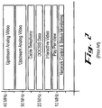
- FIG. 2 illustrates a typical reverse band and the frequencies allocated to various services that may be used by the subscriber equipment 145 for the purpose of sending reverse carrier signals.
- the combined reverse carrier signals may include a plurality of reverse carrier signals from a plurality of subscriber equipment.
- the combined carrier signals may also include a variety of signals in a plurality of frequencies.
- noise and interference is often present in the system.
- the noise signals can be viewed with test equipment as essentially a constant level, or noise floor, that most particularly affects the reverse path signals.
- the noise signals interfere with the processing of the valid carrier signals by the headend equipment.
- the presence of carrier signals in the reverse path is typically detected among the noise signals by examining the instantaneous power level of the RF signal. For example, if the power level of the RF signal is above a predetermined threshold for a predetermined amount of time, e. g. , at least 2 microseconds during any 8-microsecond window, the RF signal is treated as a valid RF carrier signal. Otherwise the reverse signal is treated as just noise and interference.
- This carrier-detect scheme works adequately for narrowband noise that has a predictable noise floor; however, wideband noise, which has a high peak to average power ratio in the time domain, can exceed the predetermined threshold for 2 microseconds in an 8- microsecond window even though its average power level is low.
- the conventional carrier-detect devices allow the transmission of noise signals more than desired.
- US 6,160,990 discloses a cable network system having GSUs installed in almost all subscriber residences. The presence of an upward transmission signal from an in-home device is monitored, and, while the upward transmission signal is detected, a transmission indication signal is supplied to the GSU. Only while the transmission indication signal is detected, the GSU sets a gate switch in an ON state. On the other hand, while no transmission indication signal is detected, the GSU keeps the gate switch in an OFF state.
- US 5,765,097 discloses a hybrid fiber-coax network that includes at least one repeater dispersed within a coax trunk that carries video information downstream to a subscriber and subscriber-originated information upstream to a fiber node. The repeater serves to digitally regenerate the subscriber-originated information to reduce ingress noise that would otherwise aggregate at the fiber node.
- the present invention is, therefore, directed to an improved carrier-detect circuit that detects a valid reverse carrier signal while significantly limiting the transmission of undesirable noise signals.
- the HFC network's reverse path signaling capacity, quality, and reliability are greatly enhanced.
- the present invention is included in the intelligent dynamic switch.
- the dynamic switch may be included in a tap or an amplifier.
- the present invention can also be included in the burst-mode analog transmitter as described in co-pending, commonly assigned, patent application Serial No. 09/840,753 (now issued as US Patent No. 6,509,994 ).
- the present invention can be included in the burst-mode digital transmitter as described in co-pending, commonly assigned, patent application Serial No. 09/840,767 (now issued as US
- IDS Intelligent Dynamic Switch
- an intelligent dynamic switch in accordance with the present invention reduces the problem of reverse ingress by allowing a reverse signal to proceed further along the reverse path only if a desired reverse signal is present.
- the IDSs will be deployed at a variety of points in the network. If an IDS determines that no desired reverse signal is present at that point in the network, it will prevent the transmission of any reverse signal, thereby preventing the transmission of reverse noise signals beyond that point in the network.
- FIG. 3 illustrates a block diagram of a communications device including the IDS with a carrier-detect device in accordance with the present invention.
- the carrier-detect device detects the presence of carrier signals included in the reverse RF signals.
- the basic elements of an exemplary IDS are shown in the block diagram of FIG. 3 .
- the concept proposed herein uses an intelligent switch to allow transmission of reverse RF signals only when the carrier-detect device 360 detects a reverse RF carrier signal.
- FIG. 3 there are five main elements related to the IDS 300. They are:
- FIG. 3 illustrates an embodiment in which the IDS 300 is included within a conventional communications device 305, such as a tap or amplifier.
- a conventional communications device 305 such as a tap or amplifier.
- forward and reverse signals are typically transmitted through the device 305.
- diplex filters 310, 315 are used to separate the forward and reverse signals.
- a high pass filter isolates the forward signals, which are typically within a band that ranges from 50 MHz to 870 MHz, and provides the forward signals to conventional forward path elements 320 associated with the communication device 305.
- the forward signals then pass through diplex filter 315 before being transmitted further downstream in a conventional manner.
- Reverse signals received at diplex filter 315 are filtered via a low pass filter and provided to the IDS 300.
- the reverse RF signals are passed from the IDS 300 to conventional reverse path elements 325 only after the carrier-detect device 360 determines that there is a valid RF carrier signal present within the reverse RF signals.
- a low pass filter in diplex filter 310 isolates the reverse signals from the forward signals and allows transmission upstream. It will be appreciated that the IDS 300 can also be a stand-alone product so long as appropriate diplex filters are used to isolate the forward and reverse signals in a two-way network.
- the IDS 300 only allows transmission of reverse RF signals when an RF carrier signal is present. This effectively blocks the transmission of noise signals until such time as the IDS 300 allows the reverse RF signals to pass through. Significantly, this device and method reduces the ingress signals that conventionally are transmitted and aggregated continuously through the reverse path and are received at the headend, and is discussed in further detail below.
- an embodiment of an IDS 300 includes an analog-to-digital (A/D) converter 350, a data buffer 355, a carrier-detect device 360, and a digital-to-analog (D/A) converter 365.
- a description of the primary elements of the IDS 300 follows.
- the A/D converter 350 receives a reverse RF signal that includes a composite of one or more reverse RF carrier signals.
- the reverse RF signals originate with one or more of the subscribers that are located downstream from the communication device 305.
- the communication device 305 is a tap
- the number of subscribers downstream from the tap may be as few as two or four
- the communication device 305 is an amplifier
- the number of subscribers downstream from the amplifier may be as high as several thousand.
- the reverse band is typically from 5 MHz to 42 MHz in U.S. cable television networks, and from 5 MHz to 65 MHz in European cable television networks.
- the composite RF signal received at the A/D converter 350 will include RF carrier signals if any of the subscriber equipment located downstream is sending signals back to the headend.
- the nature of the reverse service signals being transmitted back to the headend for processing depend upon the services that employ the reverse path, such as impulse pay-per-view (IPPV), video on demand, cable modem signals, etc. Commonly, carrier signals for different reverse services are sent in independent frequency bands as shown in FIG. 2 .
- digitization of an analog signal is known in the telecommunications industry and others, for example, as a means of converting a single baseband video or voice signal to a digital signal format.
- the conversions for these single signals are accomplished using an A/D converter having a very low sampling rate.
- reverse broadband communications signals used in a broadband cable television network require a significantly higher sampling rate.
- Nyquist theory states an analog signal must be sampled at a frequency that is greater than twice the maximum signal bandwidth in order to ensure that all information can be extracted and the inherent aliasing will not corrupt the original signal.
- the A/D and D/A converters operate with a sampling clock of typically 100 MHz with a packet size of 10 or 12-bits.
- the need for a sampling rate of 100 Megasamples per second (Ms/s), which is essentially equivalent to a 100 MHz sampling clock, is determined by understanding that the reverse RF bandwidth in the U.S. ranges from 5 MHz to 42 MHz.
- the sampling rate therefore, should be no less than 84 Ms/s, and is typically increased to 100 Ms/s because a practical anti-aliasing filter requires some transition bandwidth.
- a sampling rate of 150 Ms/s is used for a reverse band ranging from 5 MHz to 65 MHz.
- the higher sampling rate substantiates the requirement of more robust and complex A/D and D/A converters to digitize the entire bandwidth of the HFC reverse path broadband signals compared to that required for a single signal.
- the A/D converter 350 receives the reverse RF signals and digitizes the received RF signal, or waveform, producing a signal that is represented by, for example, ten parallel digital bits.
- the digital output of the A/D converter 350 is then provided to data buffer 355.
- the present invention is directed towards an improved carrier-detect device 360 that is suitable for use in the IDS 300 of FIG. 3 .
- the main function of the carrier-detect device 360 in accordance with the present invention is to accurately determine the presence of at least one desired RF carrier signal within the entire received reverse bandwidth (e.g., 5 MHz to 42 MHz) while actively eliminating the transmission of noise signals when carrier signals are not present.
- the improved carrier-detect device 360 determines if a reverse carrier signal is present by analyzing the envelope of the signal rather than conventionally analyzing the carrier signal itself.
- the improved carrier-detect device 360 extends the detection time in order to distinguish between a carrier signal and a noise signal having a very high power level, while also lowering the electronic component requirement. More specifically, a carrier signal is conventionally detected by analyzing the reverse signal over short durations of time, for example, 2 microseconds. When the power level of the carrier signal is determined to be high during this 2-microsecond duration, a carrier signal is determined to be present. As mentioned, however, the high power level may not be a valid carrier signal and may just be an increased level of noise signals resulting in an error in the detection of a carrier signal. By extending the detection time from 2 microseconds to, for example, 10 to 20 microseconds, previously detected noise signals are significantly minimized.
- a minimum valid DOCSIS burst signal carries 16 byes of data and the burst duration is approximately 12.5 microseconds for a 2.56 Mbps rate.
- the detection time in accordance with the present invention can, therefore, be extended from 2 microseconds to 10 microseconds and still adequately detect the presence of a carrier signal.
- FIG. 4 illustrates the improved carrier-detect device 360 in accordance with the present invention.
- An exemplary embodiment of the carrier-detect device 360 includes a peak detector/envelope filter 405; an A/D converter 410; and a carrier-detect logic circuit 415.
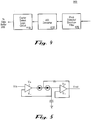
- FIG. 5 is an example of a block diagram of the peak detector/envelope filter 405 that is suitable for use in the carrier-detect device 360. Accordingly, the present invention detects the presence of a valid carrier signal by analyzing the symbols, or envelope, of the carrier signal instead of by the power level of the carrier signal itself.
- FIG. 6 illustrates a reverse RF signal displayed by a spectrum analyzer. Graph 600 displays a typical reverse signal including carrier signals. As mentioned,, the reverse signal itself is conventionally analyzed to detect the presence of a carrier signal. Symbols are displayed in graph 605. A symbol comprises reverse signals during a period of time. The carrier-detect device 360 of the present invention essentially analyzes the symbols of the reverse signal.
- the output of the peak detector/envelope filter 405 is displayed in graph 610.
- 10 microseconds of envelope signals in graph 610 comprise 10 microseconds of peak-detected symbols of graph 605, which comprise 10 microseconds of carrier signals shown in graph 600.
- the detection time can vary.
- the carrier-detect device 360 of the present invention extends the detection time in comparison with conventional methods as shown in FIG. 6 , thereby allowing valid carrier signals to be detected while eliminating detection errors of high-power noise signals that occur during a short duration time.
- the values of the capacitor and resistor should be chosen to correspond with a predetermined carrier-signal detection time, for example, from 10 microseconds to 20 microseconds. It will also be appreciated that there are several ways to implement a circuit that detects the peak voltage of the input waveform and filters out all extraneous signals.
- the A/D converter 410 receives the filtered peak envelope signal and digitizes the received signal.
- the A/D converter 410 may utilize, for example, 20 MHz 8-bit sampling. It will be appreciated that since the envelope signal provided by the peak detector/envelope filter 405 corresponds to a much lower frequency in comparison with the received analog signals, the A/D converter 410 required is less complex, thereby rendering the use of a much less expensive converter. It will also be appreciated that the sampling frequency and number of bits are arbitrary and are not intended to limit the scope of the invention.
- the digitized signal is subsequently provided to the carrier-detect logic circuit 415.
- FIG. 7 is a block diagram illustrating an embodiment of the carrier-detect logic circuit 415.
- a threshold detection circuit 710 determines whether the digitized carrier envelope has exceeded a predetermined threshold level during the detection time (i.e., 10 to 20 microseconds). Counters 715 count the duration of the "carrier envelope detected to be above the threshold level". Accordingly, the counters 715 enhance the filtering out of spurious noise signals that are at times seen on the carrier envelope.
- carrier output enable circuit 720 is set high and an enable signal is provided to a data buffer 355 ( FIG. 3 ). Subsequently, the delayed reverse signals are allowed to pass through the dynamic switch 300.
- Data buffers are well known in the art and are easily designed depending upon their application.
- a low-cost digital data buffer that uses registers or random access memory (RAM) introduces a delay that is necessary to give the carrier-detect device 360 sufficient time to detect the presence of a desired RF carrier signal.
- a 10-bit 800 samples stage first-in-first-out (FIFO) delay line 355 is used to introduce the delay.
- FIFO first-in-first-out
- the carrier-detect device 360 controls the data buffer 355 to allow the delayed digital signals to pass through.
- the digital signals are provided to the D/A converter 365 where they are converted back to analog RF signals for processing by the conventional reverse path elements 325.
- the present invention provides an improved apparatus and method for detecting the presence of a valid carrier signal.
- the improved carrier-detect device 360 takes into consideration the potential for validating invalid carrier signals, such as when noise signals are of great duration and power level.
Landscapes
- Engineering & Computer Science (AREA)
- Multimedia (AREA)
- Signal Processing (AREA)
- Two-Way Televisions, Distribution Of Moving Picture Or The Like (AREA)
- Digital Transmission Methods That Use Modulated Carrier Waves (AREA)
Claims (7)
- Verfahren zum Erkennen von wenigstens einem Trägersignal in einem Rückwärtssignal, das Trägersignale und Rauschsignale enthält, in einem Kommunikationssystem (100), das Vorwärts- und Rückwärtssignale überträgt, wobei die Rückwärtssignale als eine analoge Wellenform dargestellt werden, wobei das Verfahren die folgenden Schritte beinhaltet:Digitalisieren des Rückwärtssignals zum Bereitstellen eines digitalen Signals mit einer vorbestimmten Anzahl von digitalen Bits;Verzögern der Mehrzahl von digitalen Bits;Erkennen, wenn wenigstens ein Rückwärtsträgersignal in dem Rückwärtssignal vorliegt, durch:Erkennen eines Spitzenpegels der analogen Wellenform während einer Erkennungsperiode und zum Bereitstellen eines Spitzenhüllkurvensignals;Digitalisieren des Spitzenhüllkurvensignals zum Bereitstellen eines digitalisierten Signals;Vergleichen des digitalisierten Signals mit einem Schwellenpegelsignal;Zählen der Instanzen während der Erkennungsperiode, in denen das digitalisierte Signal das Schwellenpegelsignal übersteigt; undBereitstellen eines Freigabesignals, das die Anwesenheit des wenigstens einen Rückkehrträgersignals anzeigt, wenn die Anzahl von Instanzen eine Schwellenzahl übersteigt;Freigeben der verzögerten Mehrzahl von digitalen Bits als Reaktion auf das erste Freigabesignal; undKonvertieren der verzögerten Mehrzahl von digitalen Bits zurück in das als analoge Wellenform dargestellte Rückwärtssignal.
- Verfahren nach Anspruch 1, wobei das Bereitstellen des Freigabesignals eine weitere Übertragung der Rückwärtssignale zulässt.
- Dynamischer Schalter (300) zum Erkennen von wenigstens einem Trägersignal in einem Rückwärtssignal, das Trägersignale und Rauschsignale enthält, die in einem Kommunikationssystem (100) übertragen werden, wobei der dynamische Schalter Folgendes umfasst:Digitalisierungsmittel (350) zum Konvertieren eines Rückwärtssignals in ein digitales Signal mit einer vorbestimmten Anzahl von digitalen Bits;Erkennungsmittel (360) zum Erkennen, wenn wenigstens ein Rückwärtsträgersignal in dem Rückwärtssignal anwesend ist, und zum Bereitstellen eines Freigabesignals, das die Anwesenheit des wenigstens einen Rückwärtsträgersignals anzeigt;einen Puffer (355) zum Verzögern der Mehrzahl von digitalen Bits und zum Freisetzen der verzögerten Mehrzahl von digitalen Bits als Reaktion auf das Freigabesignal; undKonvertierungsmittel (365) zum Konvertieren der verzögerten Mehrzahl von digitalen Bits zurück in das Rückwärtssignal;wobei das Rückwärtssignal als analoge Wellenform dargestellt wird und das Erkennungsmittel (360) Folgendes umfasst:einen Spitzendetektor (405) zum Erkennen eines Spitzenpegels der analogen Wellenform und zum Bereitstellen eines Spitzenhüllkurvensignals;einen Analog-Digital-Konverter (410) zum Digitalisieren des Spitzenhüllkurvensignals; undeine Trägererkennungslogikschaltung (415) zum Feststellen, ob das digitalisierte Spitzenhüllkurvensignal das wenigstens eine Trägersignal enthält, durch Vergleichen des digitalisierten Spitzenhüllkurvensignals mit einem Schwellenpegel während einer Erkennungsperiode und zum Bereitstellen des Freigabesignals, wenn das wenigstens eine Trägersignal erkannt wird.
- Dynamischer Schalter nach Anspruch 3, wobei das Erkennungsmittel (360) ferner Folgendes umfasst:einen Schwellendetektor (710) zum Vergleichen des digitalisierten Spitzenhüllkurvensignals mit dem Schwellenpegel;einen Zähler (715) zum Bereitstellen einer Zahl gemäß dem digitalisierten Spitzenhüllkurvensignal über dem Schwellenpegel während der Erkennungsperiode; undeine Trägerausgabefreigabeschaltung (720) zum Bereitstellen des Freigabesignals, wenn die Zahl des digitalisierten Spitzenhüllkurvensignals über dem Schwellenpegel eine vorbestimmte Zahl übersteigt.
- Dynamischer Schalter nach Anspruch 3 oder Anspruch 4, der ferner Folgendes umfasst:einen Eingangsport zum Empfangen eines ersten Rückwärtssignals von einem ersten Teil des Kommunikationssystems, wobei das erste Rückwärtssignal als analoge Wellenform dargestellt wird;wobei das Digitalisierungsmittel einen Analog-Digital-Konverter zum Konvertieren des ersten Rückwärtssignals in ein digitales Signal umfasst, wobei das digitale Signal eine Mehrzahl von digitalen Bits beinhaltet;einen Digital-Analog-Konverter (365) zum Empfangen der Mehrzahl von digitalen Bits von dem Puffer (355) und zum Konvertieren der Mehrzahl von digitalen Bits in ein zweites Rückwärtssignal entsprechend dem ersten Rückwärtssignal; undeinen Ausgangsport zum Bereitstellen des zweiten Rückwärtssignals einem zweiten Teil des Kommunikationssystems.
- Kommunikationsgerät (305) zur Verwendung in einem Kommunikationssystem (100) mit Vorwärts- und Rückwärtspfaden zum Übertragen von Vorwärts- bzw. Rückwärtssignalen, wobei die Rückwärtssignale Trägersignale und Rauschsignale enthalten, wobei das Kommunikationsgerät Folgendes umfasst:ein erstes Diplex-Filter (310) mit einem Hochpassfilter und einem Tiefpassfilter, wobei das Hochpassfilter zum Isolieren der Vorwärtssignale dient und das Tiefpassfilter zum Isolieren der Rückwärtssignale dient;Vorwärtspfadelemente (320), gekoppelt mit dem Hochpassfilter des ersten Diplex-Filters (310) zur Verarbeitung;ein zweites Diplex-Filter (315) mit einem Hochpassfilter und einem Tiefpassfilter, wobei das Hochpassfilter mit den Vorwärtspfadelementen (320) gekoppelt ist, um die verarbeiteten Vorwärtssignale dem Vorwärtspfad bereitzustellen, und das Tiefpassfilter zum Empfangen von Rückwärtssignalen dient;einen dynamischen Schalter (300) nach einem der Ansprüche 3 bis 5; undRückwärtspfadelemente (325), gekoppelt mit dem dynamischen Schalter (300) zum Verarbeiten und zum Bereitstellen der verarbeiteten Rückwärtssignals dem Tiefpassfilter des ersten Filters (310),so dass nach dem Erkennen des wenigstens einen Rückwärtsträgersignals das Rückwärtssignal den Rückwärtspfadelementen (325) bereitgestellt wird.
- Kommunikationssystem (100), das Headend-Ausrüstung (105), ein Zweiweg-Netzwerk, Abonnentenausrüstung (145) und ein Kommunikationsgerät nach Anspruch 6 umfasst.
Applications Claiming Priority (3)
| Application Number | Priority Date | Filing Date | Title |
|---|---|---|---|
| US213051 | 2002-08-06 | ||
| US10/213,051 US6721352B2 (en) | 2002-08-06 | 2002-08-06 | Method and device for detecting the presence of a carrier signal transmitted in the reverse RF path |
| PCT/US2003/024401 WO2004014010A2 (en) | 2002-08-06 | 2003-08-05 | A method and device for detecting the presence of a carrier signal transmitted in the reverse rf path |
Publications (3)
| Publication Number | Publication Date |
|---|---|
| EP1535436A2 EP1535436A2 (de) | 2005-06-01 |
| EP1535436A4 EP1535436A4 (de) | 2010-05-26 |
| EP1535436B1 true EP1535436B1 (de) | 2018-03-28 |
Family
ID=31494401
Family Applications (1)
| Application Number | Title | Priority Date | Filing Date |
|---|---|---|---|
| EP03767173.2A Expired - Lifetime EP1535436B1 (de) | 2002-08-06 | 2003-08-05 | Verfahren und einrichtung zur erfassung des vorliegens eines auf einem rückwärts-rf-pfades gesendeten trägersignals |
Country Status (3)
| Country | Link |
|---|---|
| US (1) | US6721352B2 (de) |
| EP (1) | EP1535436B1 (de) |
| WO (1) | WO2004014010A2 (de) |
Families Citing this family (10)
| Publication number | Priority date | Publication date | Assignee | Title |
|---|---|---|---|---|
| US6976042B2 (en) * | 2002-05-03 | 2005-12-13 | Scientific-Atlanta, Inc. | Low cost white noise generator |
| US20060271986A1 (en) * | 2005-05-23 | 2006-11-30 | Mark Vogel | Methods, gating devices, and computer program products for determining a noise source in a communication network |
| US20080287673A1 (en) * | 2005-06-15 | 2008-11-20 | Parthasaradhi Reddy Bandk | Cefdinir process |
| RU2474972C2 (ru) * | 2006-01-17 | 2013-02-10 | Конинклейке Филипс Электроникс Н.В. | Обнаружение присутствия телевизионных сигналов, погруженных в шум, с использованием набора инструментальных средств циклостационарности |
| US7885542B2 (en) | 2006-07-07 | 2011-02-08 | Riggsby Robert R | Format converter with smart multitap and upstream signal regulator |
| US7903972B2 (en) | 2006-07-07 | 2011-03-08 | Riggsby Robert R | Format converter with smart multitap |
| US7783195B2 (en) | 2006-07-07 | 2010-08-24 | Scientific-Atlanta, Llc | Format converter with smart multitap with digital forward and reverse |
| US8270834B2 (en) * | 2007-06-13 | 2012-09-18 | West Jr Lamar E | Frequency modulated burst mode optical system |
| US20080310846A1 (en) * | 2007-06-13 | 2008-12-18 | West Jr Lamar E | Frequency modulated burst mode transmitter |
| CN117240411B (zh) * | 2023-11-15 | 2024-01-30 | 湖南中电星河电子有限公司 | 突发帧捕获方法、装置及设备 |
Citations (2)
| Publication number | Priority date | Publication date | Assignee | Title |
|---|---|---|---|---|
| US5765097A (en) * | 1996-05-20 | 1998-06-09 | At & T Corp | Shared hybrid fiber-coax network having reduced ingress noise in the upstream channel transmitted via a repeater |
| US6160990A (en) * | 1996-05-13 | 2000-12-12 | Kabushiki Kaisha Toshiba | Cable network system with ingress noise suppressing function |
Family Cites Families (9)
| Publication number | Priority date | Publication date | Assignee | Title |
|---|---|---|---|---|
| US5088111A (en) * | 1989-02-28 | 1992-02-11 | First Pacific Networks | Modulation and demodulation system employing AM-PSK and FSK for communication system using digital signals |
| US5809395A (en) * | 1991-01-15 | 1998-09-15 | Rogers Cable Systems Limited | Remote antenna driver for a radio telephony system |
| JP3214159B2 (ja) * | 1993-01-22 | 2001-10-02 | 三菱電機株式会社 | キャリア検出器 |
| US5881362A (en) * | 1994-11-30 | 1999-03-09 | General Instrument Corporation Of Delaware | Method of ingress noise reduction in calbe return paths |
| DE19603403A1 (de) | 1996-01-31 | 1997-08-07 | Sel Alcatel Ag | Optisches Übertragungssystem, bei dem störende optische Interferenzen in der Zentrale reduziert sind |
| US6137607A (en) | 1998-02-23 | 2000-10-24 | Lucent Technologies Inc. | Broadband communications method and apparatus for reducing optical beat interference |
| US6598232B1 (en) * | 1998-11-10 | 2003-07-22 | Nortel Networks Limited | Hybrid amplifier-regenerator for optimizing cable network transmissions |
| EP1168745A1 (de) * | 1999-11-12 | 2002-01-02 | Mitsubishi Denki Kabushiki Kaisha | Funkvermittlungsendgerät, das bunstposition zutreffend festlegen kann, und das geringen frequenzversatz von regenerativer trägerwelle gesitzt |
| US20030121056A1 (en) * | 2001-12-21 | 2003-06-26 | Sorenson Donald C. | HFC reverse path using an intelligent dynamic switch |
-
2002
- 2002-08-06 US US10/213,051 patent/US6721352B2/en not_active Expired - Lifetime
-
2003
- 2003-08-05 EP EP03767173.2A patent/EP1535436B1/de not_active Expired - Lifetime
- 2003-08-05 WO PCT/US2003/024401 patent/WO2004014010A2/en not_active Ceased
Patent Citations (2)
| Publication number | Priority date | Publication date | Assignee | Title |
|---|---|---|---|---|
| US6160990A (en) * | 1996-05-13 | 2000-12-12 | Kabushiki Kaisha Toshiba | Cable network system with ingress noise suppressing function |
| US5765097A (en) * | 1996-05-20 | 1998-06-09 | At & T Corp | Shared hybrid fiber-coax network having reduced ingress noise in the upstream channel transmitted via a repeater |
Also Published As
| Publication number | Publication date |
|---|---|
| US6721352B2 (en) | 2004-04-13 |
| US20040028122A1 (en) | 2004-02-12 |
| WO2004014010A3 (en) | 2004-07-08 |
| EP1535436A4 (de) | 2010-05-26 |
| WO2004014010A2 (en) | 2004-02-12 |
| EP1535436A2 (de) | 2005-06-01 |
Similar Documents
| Publication | Publication Date | Title |
|---|---|---|
| US20030121056A1 (en) | HFC reverse path using an intelligent dynamic switch | |
| US6895043B1 (en) | Method and apparatus for measuring quality of upstream signal transmission of a cable modem | |
| US5412415A (en) | Distribution of digitized composite AM FDM signals | |
| US6880170B1 (en) | Ingress detection and attenuation | |
| CN100594386C (zh) | 于网络中的正交调幅信号分析 | |
| US6462851B1 (en) | Network and method for transmitting reverse analog signals by sub-sampling the digital reverse bandwidth | |
| EP2981016B1 (de) | Rauschlokalisierung in kabelbasierten kommunikationssystemen | |
| US8214871B2 (en) | Signal compression for fiber node | |
| US6509994B2 (en) | Burst-mode analog transmitter | |
| US6721352B2 (en) | Method and device for detecting the presence of a carrier signal transmitted in the reverse RF path | |
| US20100100919A1 (en) | Method for reducing upstream ingress noise in cable data system | |
| WO2001028098A2 (en) | Digital optical receiver for cable television systems | |
| US6437895B1 (en) | Digital optical transmitter with compression | |
| US6751271B2 (en) | Detecting a carrier signal by using a power averaging circuit | |
| WO2001056197A2 (en) | Digital downstream communication system | |
| US20130301692A1 (en) | Method for ranging without docsis chipset | |
| KR100813566B1 (ko) | Hfc 전송망 감시장치 | |
| US6714598B2 (en) | Burst-mode combining of reverse path radio frequency signals | |
| KR100243692B1 (ko) | 전화 선로상의 고속 데이터 송수신용 아날로그 종단 장치 | |
| KR100844316B1 (ko) | Hfc 전송망 감시장치 | |
| US20030067659A1 (en) | System for upstream broadband transmission | |
| CN101098165A (zh) | 在同轴电缆上提供高速宽带业务的方法 | |
| Fischer | Broadband Cable Transmission According to DVB-C | |
| Fischer | Broadband Cable Transmission of Digital TV Signal (DVB-C) | |
| WO2003096692A1 (en) | Noise filtering apparatus for internet service using master antenna television network |
Legal Events
| Date | Code | Title | Description |
|---|---|---|---|
| PUAI | Public reference made under article 153(3) epc to a published international application that has entered the european phase |
Free format text: ORIGINAL CODE: 0009012 |
|
| 17P | Request for examination filed |
Effective date: 20050303 |
|
| AK | Designated contracting states |
Kind code of ref document: A2 Designated state(s): AT BE BG CH CY CZ DE DK EE ES FI FR GB GR HU IE IT LI LU MC NL PT RO SE SI SK TR |
|
| RBV | Designated contracting states (corrected) |
Designated state(s): DE ES GB |
|
| RIN1 | Information on inventor provided before grant (corrected) |
Inventor name: AO, JIENING Inventor name: WEST, LAMAR, E., JR. Inventor name: KIEN, THAI-BAO, H. |
|
| A4 | Supplementary search report drawn up and despatched |
Effective date: 20100423 |
|
| RIC1 | Information provided on ipc code assigned before grant |
Ipc: H04L 25/00 20060101AFI20050302BHEP Ipc: H04L 5/14 20060101ALI20100419BHEP Ipc: H04L 27/00 20060101ALI20100419BHEP |
|
| 17Q | First examination report despatched |
Effective date: 20101008 |
|
| GRAP | Despatch of communication of intention to grant a patent |
Free format text: ORIGINAL CODE: EPIDOSNIGR1 |
|
| STAA | Information on the status of an ep patent application or granted ep patent |
Free format text: STATUS: GRANT OF PATENT IS INTENDED |
|
| INTG | Intention to grant announced |
Effective date: 20171017 |
|
| GRAS | Grant fee paid |
Free format text: ORIGINAL CODE: EPIDOSNIGR3 |
|
| GRAA | (expected) grant |
Free format text: ORIGINAL CODE: 0009210 |
|
| STAA | Information on the status of an ep patent application or granted ep patent |
Free format text: STATUS: THE PATENT HAS BEEN GRANTED |
|
| RAP1 | Party data changed (applicant data changed or rights of an application transferred) |
Owner name: CISCO TECHNOLOGY, INC. |
|
| AK | Designated contracting states |
Kind code of ref document: B1 Designated state(s): DE ES GB |
|
| REG | Reference to a national code |
Ref country code: GB Ref legal event code: FG4D |
|
| REG | Reference to a national code |
Ref country code: DE Ref legal event code: R096 Ref document number: 60351078 Country of ref document: DE |
|
| PG25 | Lapsed in a contracting state [announced via postgrant information from national office to epo] |
Ref country code: ES Free format text: LAPSE BECAUSE OF FAILURE TO SUBMIT A TRANSLATION OF THE DESCRIPTION OR TO PAY THE FEE WITHIN THE PRESCRIBED TIME-LIMIT Effective date: 20180328 |
|
| REG | Reference to a national code |
Ref country code: DE Ref legal event code: R097 Ref document number: 60351078 Country of ref document: DE |
|
| PLBE | No opposition filed within time limit |
Free format text: ORIGINAL CODE: 0009261 |
|
| STAA | Information on the status of an ep patent application or granted ep patent |
Free format text: STATUS: NO OPPOSITION FILED WITHIN TIME LIMIT |
|
| RIC2 | Information provided on ipc code assigned after grant |
Ipc: H04L 25/00 20060101AFI20050302BHEP Ipc: H04L 5/14 20060101ALI20100419BHEP Ipc: H04L 27/00 20060101ALI20100419BHEP |
|
| 26N | No opposition filed |
Effective date: 20190103 |
|
| PGFP | Annual fee paid to national office [announced via postgrant information from national office to epo] |
Ref country code: DE Payment date: 20190828 Year of fee payment: 17 |
|
| PGFP | Annual fee paid to national office [announced via postgrant information from national office to epo] |
Ref country code: GB Payment date: 20190827 Year of fee payment: 17 |
|
| REG | Reference to a national code |
Ref country code: DE Ref legal event code: R119 Ref document number: 60351078 Country of ref document: DE |
|
| GBPC | Gb: european patent ceased through non-payment of renewal fee |
Effective date: 20200805 |
|
| PG25 | Lapsed in a contracting state [announced via postgrant information from national office to epo] |
Ref country code: DE Free format text: LAPSE BECAUSE OF NON-PAYMENT OF DUE FEES Effective date: 20210302 |
|
| PG25 | Lapsed in a contracting state [announced via postgrant information from national office to epo] |
Ref country code: GB Free format text: LAPSE BECAUSE OF NON-PAYMENT OF DUE FEES Effective date: 20200805 |
|
| P01 | Opt-out of the competence of the unified patent court (upc) registered |
Effective date: 20230525 |