EP1535167B1 - Switching arrangement including time-slot buses and several buffers - Google Patents
Switching arrangement including time-slot buses and several buffers Download PDFInfo
- Publication number
- EP1535167B1 EP1535167B1 EP02756003A EP02756003A EP1535167B1 EP 1535167 B1 EP1535167 B1 EP 1535167B1 EP 02756003 A EP02756003 A EP 02756003A EP 02756003 A EP02756003 A EP 02756003A EP 1535167 B1 EP1535167 B1 EP 1535167B1
- Authority
- EP
- European Patent Office
- Prior art keywords
- data
- bus
- time
- connection table
- slot
- Prior art date
- Legal status (The legal status is an assumption and is not a legal conclusion. Google has not performed a legal analysis and makes no representation as to the accuracy of the status listed.)
- Expired - Lifetime
Links
- 239000000872 buffer Substances 0.000 title claims abstract description 24
- 230000015654 memory Effects 0.000 claims abstract description 22
- 230000001360 synchronised effect Effects 0.000 claims abstract description 7
- 230000003139 buffering effect Effects 0.000 claims abstract description 4
- 238000004891 communication Methods 0.000 claims description 6
- 230000005540 biological transmission Effects 0.000 claims description 3
- 238000000034 method Methods 0.000 description 3
- 230000000903 blocking effect Effects 0.000 description 2
- 230000001413 cellular effect Effects 0.000 description 1
- 238000010276 construction Methods 0.000 description 1
- 238000010586 diagram Methods 0.000 description 1
- 239000011159 matrix material Substances 0.000 description 1
- 239000000203 mixture Substances 0.000 description 1
- 230000007704 transition Effects 0.000 description 1
Images


Classifications
-
- H—ELECTRICITY
- H04—ELECTRIC COMMUNICATION TECHNIQUE
- H04L—TRANSMISSION OF DIGITAL INFORMATION, e.g. TELEGRAPHIC COMMUNICATION
- H04L49/00—Packet switching elements
- H04L49/10—Packet switching elements characterised by the switching fabric construction
- H04L49/102—Packet switching elements characterised by the switching fabric construction using shared medium, e.g. bus or ring
-
- H—ELECTRICITY
- H04—ELECTRIC COMMUNICATION TECHNIQUE
- H04L—TRANSMISSION OF DIGITAL INFORMATION, e.g. TELEGRAPHIC COMMUNICATION
- H04L47/00—Traffic control in data switching networks
- H04L47/50—Queue scheduling
-
- H—ELECTRICITY
- H04—ELECTRIC COMMUNICATION TECHNIQUE
- H04L—TRANSMISSION OF DIGITAL INFORMATION, e.g. TELEGRAPHIC COMMUNICATION
- H04L47/00—Traffic control in data switching networks
- H04L47/50—Queue scheduling
- H04L47/62—Queue scheduling characterised by scheduling criteria
- H04L47/624—Altering the ordering of packets in an individual queue
-
- H—ELECTRICITY
- H04—ELECTRIC COMMUNICATION TECHNIQUE
- H04Q—SELECTING
- H04Q11/00—Selecting arrangements for multiplex systems
- H04Q11/04—Selecting arrangements for multiplex systems for time-division multiplexing
-
- H—ELECTRICITY
- H04—ELECTRIC COMMUNICATION TECHNIQUE
- H04L—TRANSMISSION OF DIGITAL INFORMATION, e.g. TELEGRAPHIC COMMUNICATION
- H04L49/00—Packet switching elements
- H04L49/30—Peripheral units, e.g. input or output ports
- H04L49/3009—Header conversion, routing tables or routing tags
-
- H—ELECTRICITY
- H04—ELECTRIC COMMUNICATION TECHNIQUE
- H04L—TRANSMISSION OF DIGITAL INFORMATION, e.g. TELEGRAPHIC COMMUNICATION
- H04L49/00—Packet switching elements
- H04L49/30—Peripheral units, e.g. input or output ports
- H04L49/3018—Input queuing
-
- H—ELECTRICITY
- H04—ELECTRIC COMMUNICATION TECHNIQUE
- H04Q—SELECTING
- H04Q2213/00—Indexing scheme relating to selecting arrangements in general and for multiplex systems
- H04Q2213/13097—Numbering, addressing
-
- H—ELECTRICITY
- H04—ELECTRIC COMMUNICATION TECHNIQUE
- H04Q—SELECTING
- H04Q2213/00—Indexing scheme relating to selecting arrangements in general and for multiplex systems
- H04Q2213/13103—Memory
-
- H—ELECTRICITY
- H04—ELECTRIC COMMUNICATION TECHNIQUE
- H04Q—SELECTING
- H04Q2213/00—Indexing scheme relating to selecting arrangements in general and for multiplex systems
- H04Q2213/13106—Microprocessor, CPU
-
- H—ELECTRICITY
- H04—ELECTRIC COMMUNICATION TECHNIQUE
- H04Q—SELECTING
- H04Q2213/00—Indexing scheme relating to selecting arrangements in general and for multiplex systems
- H04Q2213/13213—Counting, timing circuits
-
- H—ELECTRICITY
- H04—ELECTRIC COMMUNICATION TECHNIQUE
- H04Q—SELECTING
- H04Q2213/00—Indexing scheme relating to selecting arrangements in general and for multiplex systems
- H04Q2213/13214—Clock signals
-
- H—ELECTRICITY
- H04—ELECTRIC COMMUNICATION TECHNIQUE
- H04Q—SELECTING
- H04Q2213/00—Indexing scheme relating to selecting arrangements in general and for multiplex systems
- H04Q2213/13292—Time division multiplexing, TDM
-
- H—ELECTRICITY
- H04—ELECTRIC COMMUNICATION TECHNIQUE
- H04Q—SELECTING
- H04Q2213/00—Indexing scheme relating to selecting arrangements in general and for multiplex systems
- H04Q2213/13299—Bus
-
- H—ELECTRICITY
- H04—ELECTRIC COMMUNICATION TECHNIQUE
- H04Q—SELECTING
- H04Q2213/00—Indexing scheme relating to selecting arrangements in general and for multiplex systems
- H04Q2213/13393—Time slot switching, T-stage, time slot interchanging, TSI
Definitions
- the present invention is related to data nodes in communication networks, in particular to transmitting independent serial data streams through synchronous Time Division Multiplexing (TDM) switches.
- TDM Time Division Multiplexing
- the lower layer of communication networks like the connectivity layer in a core network of a cellular environment could be seen as a layer of distributed resources for managing data flows.
- Switches and multiplexers are some of the main components for this purpose.
- complex communication networks managing data of different formats and varying data rates, it is of great importance that the construction of the components are flexible without being too complex.
- the switches comprise a number of serial inputs and outputs.
- the data stream of one input may be directed in its entirety to a certain output line, or it may consist of a mixture of time division multiplexed data frames that are to be distributed to several outputs.
- the different lines may be running various interfaces, e.g. E1, E2, E3 and STM-1 (figure 1). Additionally, the data speed of each input line may vary in a wide range.
- the transition of data frames in the switches is often executed by means of time slot buses (TDMs) located on the back plane of the switches.
- TDMs time slot buses
- a TDM bus has a total capacity in the size typically about 1Gbit/s, where each time slot contains 64kbit of data.
- a traditional TDM-bus application consists of a data bus (usually 8 bits), a data clock and a frame synchronisation signal.
- the time domain is divided into frames where each frame has a fixed duration (usually 125 ⁇ s).
- a frame synchronisation signal indicates the start of each frame and has a period as long as the frame duration.
- the frame synchronisation signal and the data clock come from a synchronisation master source and form the timing master signals for all transmitters and receivers that are communicating via the TDM-bus.
- the frames are divided into a fixed number (n) of time slots (TS) identified by local time-slot counters.
- the local time-slot counters are reset by the FS signal.
- data may be transmitted from a transmitter to a receiver using time division multiplexing (TDM) .
- Serial data coming from data lines are paralleled (8 bits) so that the data can be mapped into the time slots.
- the patent publication US-A-4 791 629 discloses a node of a communication network, said node comprising one time-slot bus transferring frames from a number of serial input lines located on a receiving side of the node to a number of serial output lines located on the transmitting side of the node into two data buffers for each time-slot bus at the receiving side for buffering the frames from the input lines before transmission.
- the preferred embodiment resides in a switch with I/O lines of various interfaces as shown in figure 1. There are three buses in the back plane, and the incoming data shall be distributed among them. There are 8192 time slots per frame available on each bus (66MHz), which makes 24576 time slots all together.
- the incoming data will be buffered in one set of memory blocks for each bus.
- the physical size of the memory blocks is set at 2048 bytes, which means that the system can handle a maximum of 2048 different bytes (time slots) per frame.
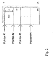
- the memories are configured in advance with a pointer value for every active line as illustrated in figure 2.
- the pointer value holds the address where the first byte in a frame is supposed to be stored. This address is loaded into a local pointer at the start of a new frame, and the pointer is incremented after data has been written to this address.
- the memory can be shared by 32 different lines, but can also be occupied by only one.
- connection table in addition to the memory blocks, there is one connection table associated with each, containing 8192 entries.
- Each entry has one address field and one control field.
- the address field points to the location in the memory where the data that are to be read from the memory can be found, while the control field holds information about e.g. whether the current timeslot is enabled, whether it is a minimum delay timeslot, etc.
- a time-slot counter When reading data from the memories, a time-slot counter is used to index the connection tables. The counter is synchronized to the bus clock, and is incremented along with the time-slots in the back plane.
- the back plane bus can transfer three different bytes at a time (one byte per bus), so the current connection table entry will relate to timeslots x, x+1, and x+2 in parallel.
- connection table The order of the bytes with which they are placed on the bus is the same as the order of their associated addresses in the connection table.
- the byte sequence of the TDM buses, and hence also the switching of data from input to output lines are controlled by where the addresses are stored in the connection table. This is pre-arranged by software according to the switching requirements concerned.
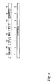
- connection table of the receiving side An entry in the connection table of the receiving side is shown in figure 4.
- the entry consists of the following fields:
- minimum delay expresses a mode of the switch in which fast data transfer is given high priority. In normal delay mode, data is stored in one frame and put on the bus in the next one. In other words, two memories are required, each containing 2048 bytes. However, in minimum delay mode, only one memory is required, since data shall be put onto the bus as fast as possible. The software programmer has to make sure that within in the same frame, a data location is not read before write-in. Minimum delay should be configured on line level and not on time-slot level.
- connection table As already mentioned, there are three buses in the back plane, and each of them can have 8192 time slots (66 MHz). This makes 24576 time slots all together.
- the data coming from the back plane will go to one memory block per bus, and a connection table then addresses these memories.
- the transmitting side connection table also contains addresses and control bits. The addresses are used to point to locations in the memory blocks, while the control bits can be used to set minimum delay.
- the size of the connection table is set at 2048 bytes, which means that the system can handle a maximum of 2048 different bytes per frame.
- the connection table is configured in advance with a size parameter and a pointer value for every active output line.
- the pointer value holds the address where the first memory address can be found. This pointer value is loaded into a local pointer at the start of a new frame, and the pointer is incremented after data has been fetched from the location the pointer is addressing.
- the connection table can be shared by 32 different lines, but can also be occupied by only one.
- the size parameter controls the connection table allocation.
- a timeslot counter is used to index the large memory when fetching data from the back plane bus. Since there are three buses, three data bytes have to be fetched in parallel. The order of the addresses in each part of the connection table then controls the output order of the corresponding bytes in the respective output lines.
- minimum delay means that only one memory block per TDM bus is used, since data shall be put onto the bus as fast as possible.
- the software programmer has to make sure that a data location is not read before write-in within in the same frame.
- connection table of the transmitting side An entry in the connection table of the transmitting side is shown in figure 6.
- the entry consists the following fields:
- the present invention provides full flexibility to cross connect time slots, and any combinations of time slots can be transferred between lines (changed order and number of time slots) depending on how the connection tables are configured to write to and read from the TDM bus.
- the delay through the node can be very low when using minimum delay. In fact, it can be less than 40 ⁇ s? for a 2Mbit/s connection. In minimum delay mode, the system is not non-blocking.
- the present invention allows for an increase in back plane speed, and high capacity can be implemented at a relatively low cost.
- redundant TDM bus, multicasting and broadcasting are permitted.
Landscapes
- Engineering & Computer Science (AREA)
- Computer Networks & Wireless Communication (AREA)
- Signal Processing (AREA)
- Time-Division Multiplex Systems (AREA)
- Use Of Switch Circuits For Exchanges And Methods Of Control Of Multiplex Exchanges (AREA)
- Small-Scale Networks (AREA)
- Communication Control (AREA)
- Data Exchanges In Wide-Area Networks (AREA)
Abstract
Description
- The present invention is related to data nodes in communication networks, in particular to transmitting independent serial data streams through synchronous Time Division Multiplexing (TDM) switches.
- The lower layer of communication networks like the connectivity layer in a core network of a cellular environment could be seen as a layer of distributed resources for managing data flows. Switches and multiplexers are some of the main components for this purpose. In complex communication networks managing data of different formats and varying data rates, it is of great importance that the construction of the components are flexible without being too complex.
- Conventionally, the switches comprise a number of serial inputs and outputs. The data stream of one input may be directed in its entirety to a certain output line, or it may consist of a mixture of time division multiplexed data frames that are to be distributed to several outputs. The different lines may be running various interfaces, e.g. E1, E2, E3 and STM-1 (figure 1). Additionally, the data speed of each input line may vary in a wide range. The transition of data frames in the switches is often executed by means of time slot buses (TDMs) located on the back plane of the switches. A TDM bus has a total capacity in the size typically about 1Gbit/s, where each time slot contains 64kbit of data.
- A traditional TDM-bus application consists of a data bus (usually 8 bits), a data clock and a frame synchronisation signal. The time domain is divided into frames where each frame has a fixed duration (usually 125 µs). A frame synchronisation signal indicates the start of each frame and has a period as long as the frame duration. The frame synchronisation signal and the data clock come from a synchronisation master source and form the timing master signals for all transmitters and receivers that are communicating via the TDM-bus. The frames are divided into a fixed number (n) of time slots (TS) identified by local time-slot counters. The local time-slot counters are reset by the FS signal. In each TS, data may be transmitted from a transmitter to a receiver using time division multiplexing (TDM) . Serial data coming from data lines are paralleled (8 bits) so that the data can be mapped into the time slots.
- In prior-art implementations of components as described above, there are limitations in the flexibility of synchronous digital switches with respect to minimum delay and configuration flexibility when combined with a non-blocking concept, multi-slot switching, high capacity and high reliability.
- The international patent application WO 99/59276 describes a synchronous digital switch with improvements compared with commercial available components using switching matrix schemes with a centralised architecture.
- The addressing method given in WO 99/59276 is superficially described. Using only a 2-bit RAM for each timeslot gives a limitation on how timeslots can be cross connected (switched) between two line boards. It is, for instance, not described how to change the order of the time slots.
- The patent publication US-A-4 791 629 discloses a node of a communication network, said node comprising one time-slot bus transferring frames from a number of serial input lines located on a receiving side of the node to a number of serial output lines located on the transmitting side of the node into two data buffers for each time-slot bus at the receiving side for buffering the frames from the input lines before transmission.
- It is an object of the present invention to provide an arrangement that eliminates the drawbacks described above. The features defined in the claims enclosed characterize this method.
- In order to make the invention more readily understandable, the discussion that follows will refer to the accompanying drawings.
- Figure 1 is a block diagram illustrating an example of serial output/input lines with variable interfaces connected to a TDM bus, e.g. in a switch,
- Figure 2 shows how pointers are allocating the memory space of a TDM buffer according to the present invention,
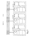
- Figure 3 shows three different TDM buffer blocks with associated connection tables at the receiving side of three TDM buses,
- Figure 4 shows an example of an entry in a connection table at the receiving side of the TDM buses according to the present invention,
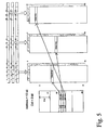
- Figure 5 shows three different TDM buffer blocks and one shared connection table at the transmitting side of three TDM buses,
- Figure 6 shows an example of an entry in a connection tables at the transmitting side of the TDM buses according to the present invention.
-
- In the following, a preferred embodiment of the present invention will be described. This is just one of many embodiments and variations within the scope of the invention defined by the independent claims enclosed, and must not be considered as limiting.
- The preferred embodiment resides in a switch with I/O lines of various interfaces as shown in figure 1. There are three buses in the back plane, and the incoming data shall be distributed among them. There are 8192 time slots per frame available on each bus (66MHz), which makes 24576 time slots all together.
- The incoming data will be buffered in one set of memory blocks for each bus. The physical size of the memory blocks is set at 2048 bytes, which means that the system can handle a maximum of 2048 different bytes (time slots) per frame. The memories are configured in advance with a pointer value for every active line as illustrated in figure 2.
- The pointer value holds the address where the first byte in a frame is supposed to be stored. This address is loaded into a local pointer at the start of a new frame, and the pointer is incremented after data has been written to this address. The memory can be shared by 32 different lines, but can also be occupied by only one.
- Referring to figure 3, in addition to the memory blocks, there is one connection table associated with each, containing 8192 entries. Each entry has one address field and one control field. The address field points to the location in the memory where the data that are to be read from the memory can be found, while the control field holds information about e.g. whether the current timeslot is enabled, whether it is a minimum delay timeslot, etc.
- When reading data from the memories, a time-slot counter is used to index the connection tables. The counter is synchronized to the bus clock, and is incremented along with the time-slots in the back plane. The back plane bus can transfer three different bytes at a time (one byte per bus), so the current connection table entry will relate to timeslots x, x+1, and x+2 in parallel.
- The order of the bytes with which they are placed on the bus is the same as the order of their associated addresses in the connection table. Thus, the byte sequence of the TDM buses, and hence also the switching of data from input to output lines are controlled by where the addresses are stored in the connection table. This is pre-arranged by software according to the switching requirements concerned.
- An entry in the connection table of the receiving side is shown in figure 4. The entry consists of the following fields:
- ADDRESS
- addressing a byte in a memory block
- EN
- enable time slot. Set to '1' if the time slot is enabled and the corresponding data shall be put onto the back plane bus.
- MIN
- Indicates if the timeslot is minimum delay.
- CPU
- Indicates if data should be fetched from a CPU register
- The term "minimum delay" expresses a mode of the switch in which fast data transfer is given high priority. In normal delay mode, data is stored in one frame and put on the bus in the next one. In other words, two memories are required, each containing 2048 bytes. However, in minimum delay mode, only one memory is required, since data shall be put onto the bus as fast as possible. The software programmer has to make sure that within in the same frame, a data location is not read before write-in. Minimum delay should be configured on line level and not on time-slot level.
- So far, only the receiving side of the TDM buses has been described. According to the present invention, a similar architecture is present at the transmitting side, as shown in figure 5. The modules shown are responsible for storing data coming from the back plane bus, and pass it on to the outgoing lines.
- As already mentioned, there are three buses in the back plane, and each of them can have 8192 time slots (66 MHz). This makes 24576 time slots all together. The data coming from the back plane will go to one memory block per bus, and a connection table then addresses these memories. As opposed to the receiving side, there is only one connection table, and not one per bus. However, the transmitting side connection table also contains addresses and control bits. The addresses are used to point to locations in the memory blocks, while the control bits can be used to set minimum delay.
- The size of the connection table is set at 2048 bytes, which means that the system can handle a maximum of 2048 different bytes per frame. The connection table is configured in advance with a size parameter and a pointer value for every active output line. The pointer value holds the address where the first memory address can be found. This pointer value is loaded into a local pointer at the start of a new frame, and the pointer is incremented after data has been fetched from the location the pointer is addressing. The connection table can be shared by 32 different lines, but can also be occupied by only one. The size parameter controls the connection table allocation.
- A timeslot counter is used to index the large memory when fetching data from the back plane bus. Since there are three buses, three data bytes have to be fetched in parallel. The order of the addresses in each part of the connection table then controls the output order of the corresponding bytes in the respective output lines.
- Also, at the transmitting side, minimum delay means that only one memory block per TDM bus is used, since data shall be put onto the bus as fast as possible. The software programmer has to make sure that a data location is not read before write-in within in the same frame.
- 32 dedicated CPU registers are available for storing idle pattern data. These patterns can be sent out on the serial lines.
- An entry in the connection table of the transmitting side is shown in figure 6. The entry consists the following fields:
- ADDRESS
- the addressing of the RAM
- MIN
- Indicates if the timeslot is minimum delay
- BUS
- "00" - fetch data from
bus 1
"01" - fetch data frombus 2
"10" - fetch data frombus 3
"11" - fetch data from a CPU register - The present invention provides full flexibility to cross connect time slots, and any combinations of time slots can be transferred between lines (changed order and number of time slots) depending on how the connection tables are configured to write to and read from the TDM bus.
- Further, the delay through the node can be very low when using minimum delay. In fact, it can be less than 40µs? for a 2Mbit/s connection. In minimum delay mode, the system is not non-blocking.
- The present invention allows for an increase in back plane speed, and high capacity can be implemented at a relatively low cost.
- Also, redundant TDM bus, multicasting and broadcasting (one transmitter and several receivers) are permitted.
-
- E1
- 2 Mbit/s data transfer method
- LINE
- Serial data lines, i.e. E1, STM-1 etc.
- PFU
- Power Feeding Unit
- STM-1
- Synchronous Transfer Mode
- TDM
- Time Division Multiplexing
Claims (9)
- An arrangement applied to a node in a communication network, said node comprising one or more time-slot buses transferring frames from a number of serial input lines located on a receiving side of the node to a number of serial output lines located on the transmitting side of the node, said arrangement comprising
one or two data buffers for each time-slot bus at the receiving side buffering the frames from the input lines before transmission,
characterized in
connection table for each time-slot bus at the receiving side, each entry in the connection table containing at least a data address pointing to a byte in the associated data buffer, the entries are arranged in the same order as their corresponding bytes are to be transferred on the data bus, and
a counter, synchronized to a clock used by the time-slot bus for transmission of time slots, indicating which byte in the associated data buffer that presently is to be read out from the data-bus buffer into a time slot in the associated data bus by indexing the entries of the connection table. - Arrangement according to claim 1,
characterized in that the data buffers are shared between all the input lines by means of respective pointers allocating one memory area in the data buffer for each of the input lines. - Arrangement according to claim 1 or 2,
characterized in that each entry in the connection table contains, in addition to the data address, a control field. - Arrangement according to any of the preceding claims,
characterized in that there is only one data buffer for each time slot bus, and, within the same frame, a data location in the buffer is not read before write-in. - An arrangement applied to a node in a communication network, said node comprising one or more time slot buses transferring frames from a number of serial input lines located on a receiving side of the node to a number of serial output lines located on the transmitting side of the node,
characterized in
one or two data buffers for each time-slot bus at the transmitting side buffering the frames from time-slot buses before forwarding to the output line,
a connection table wherein each entry in the connection table contains at least a data address pointing to a byte in one of the data buffers, the entries are arranged in the same order as their corresponding bytes are to be transferred to an output line. - Arrangement according to claim 5,
characterized in
one starting pointer per output line allocating one memory area in the connection table for each of the output lines, and pointing to the first entry in each memory area,
one indexing pointer per output line pointing at the entry in the connection table holding the address to the byte currently being fetched from one of the buffers to the associated output line. - Arrangement according to claim 5 or 6,
characterized in that each entry in the connection table contains, in addition to the data address, a control field. - Arrangement according to one of the claims 5 - 7,
characterized in that there is only one data buffer for each time-slot bus, and, within the same frame, a data location in the buffer is not read before write-in. - Arrangement according to one of the claims 5 - 8,
characterized in that there is only one data buffer for each time-slot bus, and, within the same frame, a data location in the buffer is not read before write-in.
Applications Claiming Priority (1)
| Application Number | Priority Date | Filing Date | Title |
|---|---|---|---|
| PCT/NO2002/000313 WO2004023319A1 (en) | 2002-09-06 | 2002-09-06 | Switching arrangement including time-slot buses and several buffers |
Publications (2)
| Publication Number | Publication Date |
|---|---|
| EP1535167A1 EP1535167A1 (en) | 2005-06-01 |
| EP1535167B1 true EP1535167B1 (en) | 2005-12-14 |
Family
ID=31973753
Family Applications (1)
| Application Number | Title | Priority Date | Filing Date |
|---|---|---|---|
| EP02756003A Expired - Lifetime EP1535167B1 (en) | 2002-09-06 | 2002-09-06 | Switching arrangement including time-slot buses and several buffers |
Country Status (8)
| Country | Link |
|---|---|
| US (1) | US20060002398A1 (en) |
| EP (1) | EP1535167B1 (en) |
| CN (1) | CN1662894B (en) |
| AT (1) | ATE313115T1 (en) |
| AU (1) | AU2002321955A1 (en) |
| DE (1) | DE60208087T2 (en) |
| ES (1) | ES2250686T3 (en) |
| WO (1) | WO2004023319A1 (en) |
Families Citing this family (5)
| Publication number | Priority date | Publication date | Assignee | Title |
|---|---|---|---|---|
| NO20016372D0 (en) * | 2001-12-27 | 2001-12-27 | Ericsson Telefon Ab L M | Arrangement to reduce memory requirements in a switch |
| CN1848715B (en) * | 2005-04-05 | 2010-06-16 | 中兴通讯股份有限公司 | Method, system and processing device for realizing transparent transmission of synchronous serial data in TDM network |
| CN101155132B (en) * | 2006-09-27 | 2012-07-04 | 中兴通讯股份有限公司 | Indirect real-time flux control system and its method |
| CN101370313B (en) * | 2007-08-17 | 2011-05-11 | 中兴通讯股份有限公司 | Uplink exchange circuit of asymmetric input and output port and its exchange method |
| CN101207471B (en) * | 2007-12-12 | 2011-09-21 | 上海华为技术有限公司 | Method and device for exchanging time slots |
Family Cites Families (12)
| Publication number | Priority date | Publication date | Assignee | Title |
|---|---|---|---|---|
| US4791629A (en) * | 1986-06-02 | 1988-12-13 | Ibm Corporation | Communications switching system |
| GB9012436D0 (en) * | 1990-06-04 | 1990-07-25 | Plessey Telecomm | Sdh rejustification |
| US5291482A (en) * | 1992-07-24 | 1994-03-01 | At&T Bell Laboratories | High bandwidth packet switch |
| US5495478A (en) * | 1994-11-14 | 1996-02-27 | Dsc Communications Corporation | Apparatus and method for processing asynchronous transfer mode cells |
| US5862136A (en) * | 1995-07-07 | 1999-01-19 | Northern Telecom Limited | Telecommunications apparatus and method |
| WO1999033278A2 (en) * | 1997-09-26 | 1999-07-01 | Alcatel Usa Sourcing Lp | Interface components for a telecommunications switching platform |
| DE69809224T2 (en) * | 1998-08-28 | 2003-08-28 | Ibm | Switching device with at least one switching core access element for connecting different protocol adapters |
| US6625234B1 (en) * | 1998-12-10 | 2003-09-23 | Nortel Networks Limited | Efficient implementations of proposed turbo code interleavers for third generation code division multiple access |
| US6606317B1 (en) * | 1999-09-09 | 2003-08-12 | Harris Corporation | Dual key controlled content addressable memory for accessing packet switch data buffer for multicasting data packets |
| US7110359B1 (en) * | 2001-03-05 | 2006-09-19 | Advanced Micro Devices, Inc. | System and method for dynamically updating weights of weighted round robin in output queues |
| FR2828046B1 (en) * | 2001-07-27 | 2003-10-10 | Thales Sa | TASK MANAGEMENT METHOD FOR A PACKET SWITCHING ROUTER AUTOMATION PART OF A SECURE PACKET SWITCHED TRANSMISSION NETWORK |
| US7190696B1 (en) * | 2002-03-05 | 2007-03-13 | Force10 Networks, Inc. | System and method for distributing packets among a plurality of paths to a destination |
-
2002
- 2002-09-06 DE DE60208087T patent/DE60208087T2/en not_active Expired - Lifetime
- 2002-09-06 AU AU2002321955A patent/AU2002321955A1/en not_active Abandoned
- 2002-09-06 ES ES02756003T patent/ES2250686T3/en not_active Expired - Lifetime
- 2002-09-06 AT AT02756003T patent/ATE313115T1/en not_active IP Right Cessation
- 2002-09-06 CN CN028295331A patent/CN1662894B/en not_active Expired - Fee Related
- 2002-09-06 EP EP02756003A patent/EP1535167B1/en not_active Expired - Lifetime
- 2002-09-06 US US10/526,526 patent/US20060002398A1/en not_active Abandoned
- 2002-09-06 WO PCT/NO2002/000313 patent/WO2004023319A1/en not_active Ceased
Also Published As
| Publication number | Publication date |
|---|---|
| CN1662894A (en) | 2005-08-31 |
| CN1662894B (en) | 2010-05-26 |
| US20060002398A1 (en) | 2006-01-05 |
| ATE313115T1 (en) | 2005-12-15 |
| DE60208087T2 (en) | 2006-07-13 |
| DE60208087D1 (en) | 2006-01-19 |
| AU2002321955A1 (en) | 2004-03-29 |
| ES2250686T3 (en) | 2006-04-16 |
| EP1535167A1 (en) | 2005-06-01 |
| WO2004023319A1 (en) | 2004-03-18 |
Similar Documents
| Publication | Publication Date | Title |
|---|---|---|
| US5202885A (en) | Atm exchange with copying capability | |
| US4771425A (en) | Synchoronous packet voice/data communication system | |
| EP0203165B1 (en) | Queueing protocol | |
| US5425022A (en) | Data switching nodes | |
| US4819228A (en) | Synchronous packet voice/data communication system | |
| CA2096877C (en) | High bandwidth packet switch | |
| CA2042037C (en) | Multiple access system for a communication network | |
| CA2036756C (en) | High-speed time-division switching system | |
| US6064670A (en) | Matrix for switching between two multiplex groups | |
| US20010038613A1 (en) | Time slot assigner for communication system | |
| EP1535167B1 (en) | Switching arrangement including time-slot buses and several buffers | |
| JP2711134B2 (en) | Replacement module | |
| JP3009745B2 (en) | Method of synchronous exchange of signal information | |
| US5892760A (en) | Device for binary data transfer between a time-division multiplex and a memory | |
| US5164940A (en) | Modular communication system with allocatable bandwidth | |
| EP0477242B1 (en) | Data switching nodes | |
| RU2291479C2 (en) | Commutation device containing temporary intervals bus and several buffers | |
| CN100470530C (en) | Apparatus for interconnecting printed circuit boards communicating with each other by a time-division multiplexed data bus | |
| US20050068991A1 (en) | Managing payload specific latencies in a cross-connect system | |
| EP1461917B1 (en) | Method for reducing the amount of needed memory in a tdm switch system | |
| RU2295149C2 (en) | Method for decreasing load on bus in synchronous data bus system | |
| GB2286099A (en) | Modular communication system with allocatable bandwidth | |
| JP3481841B2 (en) | Time division multiplexed data / cell conversion circuit and cell / time division multiplexed data conversion circuit | |
| JPH0113799B2 (en) | ||
| JPS6145649A (en) | Multi-drop communication system in line multiplex type loop network |
Legal Events
| Date | Code | Title | Description |
|---|---|---|---|
| PUAI | Public reference made under article 153(3) epc to a published international application that has entered the european phase |
Free format text: ORIGINAL CODE: 0009012 |
|
| 17P | Request for examination filed |
Effective date: 20050224 |
|
| AK | Designated contracting states |
Kind code of ref document: A1 Designated state(s): AT BE BG CH CY CZ DE DK EE ES FI FR GB GR IE IT LI LU MC NL PT SE SK TR |
|
| AX | Request for extension of the european patent |
Extension state: AL LT LV MK RO SI |
|
| GRAP | Despatch of communication of intention to grant a patent |
Free format text: ORIGINAL CODE: EPIDOSNIGR1 |
|
| GRAS | Grant fee paid |
Free format text: ORIGINAL CODE: EPIDOSNIGR3 |
|
| GRAA | (expected) grant |
Free format text: ORIGINAL CODE: 0009210 |
|
| AK | Designated contracting states |
Kind code of ref document: B1 Designated state(s): AT BE BG CH CY CZ DE DK EE ES FI FR GB GR IE IT LI LU MC NL PT SE SK TR |
|
| PG25 | Lapsed in a contracting state [announced via postgrant information from national office to epo] |
Ref country code: IT Free format text: LAPSE BECAUSE OF FAILURE TO SUBMIT A TRANSLATION OF THE DESCRIPTION OR TO PAY THE FEE WITHIN THE PRESCRIBED TIME-LIMIT;WARNING: LAPSES OF ITALIAN PATENTS WITH EFFECTIVE DATE BEFORE 2007 MAY HAVE OCCURRED AT ANY TIME BEFORE 2007. THE CORRECT EFFECTIVE DATE MAY BE DIFFERENT FROM THE ONE RECORDED. Effective date: 20051214 Ref country code: CH Free format text: LAPSE BECAUSE OF FAILURE TO SUBMIT A TRANSLATION OF THE DESCRIPTION OR TO PAY THE FEE WITHIN THE PRESCRIBED TIME-LIMIT Effective date: 20051214 Ref country code: NL Free format text: LAPSE BECAUSE OF FAILURE TO SUBMIT A TRANSLATION OF THE DESCRIPTION OR TO PAY THE FEE WITHIN THE PRESCRIBED TIME-LIMIT Effective date: 20051214 Ref country code: LI Free format text: LAPSE BECAUSE OF FAILURE TO SUBMIT A TRANSLATION OF THE DESCRIPTION OR TO PAY THE FEE WITHIN THE PRESCRIBED TIME-LIMIT Effective date: 20051214 Ref country code: FI Free format text: LAPSE BECAUSE OF FAILURE TO SUBMIT A TRANSLATION OF THE DESCRIPTION OR TO PAY THE FEE WITHIN THE PRESCRIBED TIME-LIMIT Effective date: 20051214 Ref country code: CZ Free format text: LAPSE BECAUSE OF FAILURE TO SUBMIT A TRANSLATION OF THE DESCRIPTION OR TO PAY THE FEE WITHIN THE PRESCRIBED TIME-LIMIT Effective date: 20051214 Ref country code: AT Free format text: LAPSE BECAUSE OF FAILURE TO SUBMIT A TRANSLATION OF THE DESCRIPTION OR TO PAY THE FEE WITHIN THE PRESCRIBED TIME-LIMIT Effective date: 20051214 Ref country code: BE Free format text: LAPSE BECAUSE OF FAILURE TO SUBMIT A TRANSLATION OF THE DESCRIPTION OR TO PAY THE FEE WITHIN THE PRESCRIBED TIME-LIMIT Effective date: 20051214 Ref country code: SK Free format text: LAPSE BECAUSE OF FAILURE TO SUBMIT A TRANSLATION OF THE DESCRIPTION OR TO PAY THE FEE WITHIN THE PRESCRIBED TIME-LIMIT Effective date: 20051214 |
|
| REG | Reference to a national code |
Ref country code: GB Ref legal event code: FG4D |
|
| REG | Reference to a national code |
Ref country code: CH Ref legal event code: EP |
|
| REG | Reference to a national code |
Ref country code: IE Ref legal event code: FG4D |
|
| REF | Corresponds to: |
Ref document number: 60208087 Country of ref document: DE Date of ref document: 20060119 Kind code of ref document: P |
|
| PG25 | Lapsed in a contracting state [announced via postgrant information from national office to epo] |
Ref country code: BG Free format text: LAPSE BECAUSE OF FAILURE TO SUBMIT A TRANSLATION OF THE DESCRIPTION OR TO PAY THE FEE WITHIN THE PRESCRIBED TIME-LIMIT Effective date: 20060314 Ref country code: DK Free format text: LAPSE BECAUSE OF FAILURE TO SUBMIT A TRANSLATION OF THE DESCRIPTION OR TO PAY THE FEE WITHIN THE PRESCRIBED TIME-LIMIT Effective date: 20060314 Ref country code: GR Free format text: LAPSE BECAUSE OF FAILURE TO SUBMIT A TRANSLATION OF THE DESCRIPTION OR TO PAY THE FEE WITHIN THE PRESCRIBED TIME-LIMIT Effective date: 20060314 Ref country code: SE Free format text: LAPSE BECAUSE OF FAILURE TO SUBMIT A TRANSLATION OF THE DESCRIPTION OR TO PAY THE FEE WITHIN THE PRESCRIBED TIME-LIMIT Effective date: 20060314 |
|
| REG | Reference to a national code |
Ref country code: ES Ref legal event code: FG2A Ref document number: 2250686 Country of ref document: ES Kind code of ref document: T3 |
|
| PG25 | Lapsed in a contracting state [announced via postgrant information from national office to epo] |
Ref country code: PT Free format text: LAPSE BECAUSE OF FAILURE TO SUBMIT A TRANSLATION OF THE DESCRIPTION OR TO PAY THE FEE WITHIN THE PRESCRIBED TIME-LIMIT Effective date: 20060515 |
|
| NLV1 | Nl: lapsed or annulled due to failure to fulfill the requirements of art. 29p and 29m of the patents act | ||
| REG | Reference to a national code |
Ref country code: CH Ref legal event code: PL |
|
| PG25 | Lapsed in a contracting state [announced via postgrant information from national office to epo] |
Ref country code: IE Free format text: LAPSE BECAUSE OF NON-PAYMENT OF DUE FEES Effective date: 20060906 |
|
| PG25 | Lapsed in a contracting state [announced via postgrant information from national office to epo] |
Ref country code: MC Free format text: LAPSE BECAUSE OF NON-PAYMENT OF DUE FEES Effective date: 20060930 |
|
| PLBE | No opposition filed within time limit |
Free format text: ORIGINAL CODE: 0009261 |
|
| STAA | Information on the status of an ep patent application or granted ep patent |
Free format text: STATUS: NO OPPOSITION FILED WITHIN TIME LIMIT |
|
| 26N | No opposition filed |
Effective date: 20060915 |
|
| EN | Fr: translation not filed | ||
| REG | Reference to a national code |
Ref country code: IE Ref legal event code: MM4A |
|
| PG25 | Lapsed in a contracting state [announced via postgrant information from national office to epo] |
Ref country code: FR Free format text: LAPSE BECAUSE OF FAILURE TO SUBMIT A TRANSLATION OF THE DESCRIPTION OR TO PAY THE FEE WITHIN THE PRESCRIBED TIME-LIMIT Effective date: 20070202 |
|
| PG25 | Lapsed in a contracting state [announced via postgrant information from national office to epo] |
Ref country code: EE Free format text: LAPSE BECAUSE OF FAILURE TO SUBMIT A TRANSLATION OF THE DESCRIPTION OR TO PAY THE FEE WITHIN THE PRESCRIBED TIME-LIMIT Effective date: 20051214 |
|
| PG25 | Lapsed in a contracting state [announced via postgrant information from national office to epo] |
Ref country code: LU Free format text: LAPSE BECAUSE OF NON-PAYMENT OF DUE FEES Effective date: 20060906 Ref country code: TR Free format text: LAPSE BECAUSE OF FAILURE TO SUBMIT A TRANSLATION OF THE DESCRIPTION OR TO PAY THE FEE WITHIN THE PRESCRIBED TIME-LIMIT Effective date: 20051214 |
|
| PG25 | Lapsed in a contracting state [announced via postgrant information from national office to epo] |
Ref country code: FR Free format text: LAPSE BECAUSE OF FAILURE TO SUBMIT A TRANSLATION OF THE DESCRIPTION OR TO PAY THE FEE WITHIN THE PRESCRIBED TIME-LIMIT Effective date: 20051214 Ref country code: CY Free format text: LAPSE BECAUSE OF FAILURE TO SUBMIT A TRANSLATION OF THE DESCRIPTION OR TO PAY THE FEE WITHIN THE PRESCRIBED TIME-LIMIT Effective date: 20051214 |
|
| PGFP | Annual fee paid to national office [announced via postgrant information from national office to epo] |
Ref country code: ES Payment date: 20150928 Year of fee payment: 14 Ref country code: GB Payment date: 20150928 Year of fee payment: 14 |
|
| PGFP | Annual fee paid to national office [announced via postgrant information from national office to epo] |
Ref country code: DE Payment date: 20150929 Year of fee payment: 14 |
|
| REG | Reference to a national code |
Ref country code: DE Ref legal event code: R119 Ref document number: 60208087 Country of ref document: DE |
|
| GBPC | Gb: european patent ceased through non-payment of renewal fee |
Effective date: 20160906 |
|
| PG25 | Lapsed in a contracting state [announced via postgrant information from national office to epo] |
Ref country code: DE Free format text: LAPSE BECAUSE OF NON-PAYMENT OF DUE FEES Effective date: 20170401 Ref country code: GB Free format text: LAPSE BECAUSE OF NON-PAYMENT OF DUE FEES Effective date: 20160906 |
|
| PG25 | Lapsed in a contracting state [announced via postgrant information from national office to epo] |
Ref country code: ES Free format text: LAPSE BECAUSE OF NON-PAYMENT OF DUE FEES Effective date: 20160907 |
|
| REG | Reference to a national code |
Ref country code: ES Ref legal event code: FD2A Effective date: 20181126 |