EP1533857B1 - Electrowetting battery having a nanostructured electrode surface - Google Patents
Electrowetting battery having a nanostructured electrode surface Download PDFInfo
- Publication number
- EP1533857B1 EP1533857B1 EP04256701A EP04256701A EP1533857B1 EP 1533857 B1 EP1533857 B1 EP 1533857B1 EP 04256701 A EP04256701 A EP 04256701A EP 04256701 A EP04256701 A EP 04256701A EP 1533857 B1 EP1533857 B1 EP 1533857B1
- Authority
- EP
- European Patent Office
- Prior art keywords
- battery
- electrode
- liquid
- electrolyte fluid
- laser
- Prior art date
- Legal status (The legal status is an assumption and is not a legal conclusion. Google has not performed a legal analysis and makes no representation as to the accuracy of the status listed.)
- Expired - Lifetime
Links
- 239000007788 liquid Substances 0.000 claims description 27
- 239000003792 electrolyte Substances 0.000 claims description 25
- 239000012530 fluid Substances 0.000 claims description 17
- 239000002086 nanomaterial Substances 0.000 claims description 16
- 239000000463 material Substances 0.000 description 13
- 238000000034 method Methods 0.000 description 8
- 239000000758 substrate Substances 0.000 description 6
- 239000000853 adhesive Substances 0.000 description 4
- 230000001070 adhesive effect Effects 0.000 description 4
- 238000006243 chemical reaction Methods 0.000 description 4
- 230000008685 targeting Effects 0.000 description 4
- 238000003491 array Methods 0.000 description 3
- 230000035515 penetration Effects 0.000 description 3
- XUIMIQQOPSSXEZ-UHFFFAOYSA-N Silicon Chemical compound [Si] XUIMIQQOPSSXEZ-UHFFFAOYSA-N 0.000 description 2
- 230000008901 benefit Effects 0.000 description 2
- 239000010410 layer Substances 0.000 description 2
- 239000003973 paint Substances 0.000 description 2
- 230000008569 process Effects 0.000 description 2
- 229910052710 silicon Inorganic materials 0.000 description 2
- 239000010703 silicon Substances 0.000 description 2
- JOYRKODLDBILNP-UHFFFAOYSA-N Ethyl urethane Chemical compound CCOC(N)=O JOYRKODLDBILNP-UHFFFAOYSA-N 0.000 description 1
- 229920000122 acrylonitrile butadiene styrene Polymers 0.000 description 1
- 230000003213 activating effect Effects 0.000 description 1
- 239000011149 active material Substances 0.000 description 1
- 230000009286 beneficial effect Effects 0.000 description 1
- 230000008859 change Effects 0.000 description 1
- 230000007423 decrease Effects 0.000 description 1
- 239000003989 dielectric material Substances 0.000 description 1
- 230000004069 differentiation Effects 0.000 description 1
- 239000008151 electrolyte solution Substances 0.000 description 1
- 238000005530 etching Methods 0.000 description 1
- 238000010304 firing Methods 0.000 description 1
- 239000004811 fluoropolymer Substances 0.000 description 1
- 230000006870 function Effects 0.000 description 1
- 150000002500 ions Chemical class 0.000 description 1
- 230000001788 irregular Effects 0.000 description 1
- 238000001459 lithography Methods 0.000 description 1
- 238000004519 manufacturing process Methods 0.000 description 1
- 230000007246 mechanism Effects 0.000 description 1
- 238000007254 oxidation reaction Methods 0.000 description 1
- 238000010422 painting Methods 0.000 description 1
- 238000006722 reduction reaction Methods 0.000 description 1
- 238000000926 separation method Methods 0.000 description 1
- 239000002356 single layer Substances 0.000 description 1
Images

Classifications
-
- H—ELECTRICITY
- H01—ELECTRIC ELEMENTS
- H01M—PROCESSES OR MEANS, e.g. BATTERIES, FOR THE DIRECT CONVERSION OF CHEMICAL ENERGY INTO ELECTRICAL ENERGY
- H01M4/00—Electrodes
- H01M4/02—Electrodes composed of, or comprising, active material
-
- F—MECHANICAL ENGINEERING; LIGHTING; HEATING; WEAPONS; BLASTING
- F42—AMMUNITION; BLASTING
- F42C—AMMUNITION FUZES; ARMING OR SAFETY MEANS THEREFOR
- F42C19/00—Details of fuzes
-
- H—ELECTRICITY
- H01—ELECTRIC ELEMENTS
- H01M—PROCESSES OR MEANS, e.g. BATTERIES, FOR THE DIRECT CONVERSION OF CHEMICAL ENERGY INTO ELECTRICAL ENERGY
- H01M6/00—Primary cells; Manufacture thereof
- H01M6/30—Deferred-action cells
- H01M6/32—Deferred-action cells activated through external addition of electrolyte or of electrolyte components
-
- H—ELECTRICITY
- H01—ELECTRIC ELEMENTS
- H01M—PROCESSES OR MEANS, e.g. BATTERIES, FOR THE DIRECT CONVERSION OF CHEMICAL ENERGY INTO ELECTRICAL ENERGY
- H01M6/00—Primary cells; Manufacture thereof
- H01M6/30—Deferred-action cells
- H01M6/36—Deferred-action cells containing electrolyte and made operational by physical means, e.g. thermal cells
-
- H—ELECTRICITY
- H01—ELECTRIC ELEMENTS
- H01M—PROCESSES OR MEANS, e.g. BATTERIES, FOR THE DIRECT CONVERSION OF CHEMICAL ENERGY INTO ELECTRICAL ENERGY
- H01M6/00—Primary cells; Manufacture thereof
- H01M6/30—Deferred-action cells
Definitions
- the present invention relates generally to batteries and, more particularly, to batteries having at least one nanostructured electrode surface.
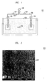
- illustrative liquid-cell battery 101 is characterized by an electrolyte liquid 102 which provides a mechanism for an electrical charge to flow in direction 103 between a positive electrode 104 and a negative electrode 105.
- electrolyte liquid 102 which provides a mechanism for an electrical charge to flow in direction 103 between a positive electrode 104 and a negative electrode 105.
- the positive electrode thus receives electrons from the external circuit 106.
- These electrons then react with the materials of the positive electrode 104 in reduction reactions that generate the flow of a charge to the negative electrode 105 via ions in the electrolyte liquid 102.
- oxidation reactions between the materials of the negative electrode 104 and the charge flowing through the electrolyte fluid 102 result in surplus electrons that are released to the external circuit 106.
- the active materials of the positive and negative electrodes 104 and 105 eventually become depleted and the reactions slow down until the battery is no longer capable of supplying electrons. At this point the battery is discharged. It is well known that, even when a liquid-cell battery is not inserted into an electrical circuit, there is often a low level reaction with the electrodes 104 and 105 that can eventually deplete the material of the electrodes. Thus, a battery can become depleted over a period of time even when it is not in active use in an electrical circuit. This period of time will vary depending on the electrolyte fluid used and the materials of the electrodes.
- a battery comprises an electrode having at least one nanostructured surface.
- the nanostructured surface is disposed in a way such that an electrolyte fluid of the battery is prevented from contacting the electrode, thus preventing discharge of the battery when the battery is not in use.
- the electrolyte fluid is caused to penetrate the nanostructured surface and to contact the electrode, thus activating the battery. Accordingly, when the activated battery is inserted into an electrical circuit, electrons will flow along the circuit.
- the battery is an integrated part of an electronics package.
- the battery is manufactured as a separate device and is then brought into contact with the electronics package.
- the electronics package and an attached battery are disposed in a projectile that is used as a military targeting device.
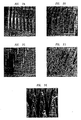
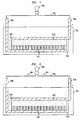
- FIG. 2 shows an illustrative nanopost pattern 201 with each nanopost 209 having a diameter of less than 1 micrometer. While FIG. 2 shows nanoposts 209 formed in a somewhat conical shape, other shapes and sizes are also achievable. In fact, cylindrical nanopost arrays have been produced with each nanopost having a diameter of less than 10 nm. Specifically, FIGs. 3A-3E show different illustrative arrangements of nanoposts produced using various methods and further show that such various diameter nanoposts can be fashioned with different degrees of regularity. Moreover, these figures show that it is possible to produce nanoposts having various diameters separated by various distances. An illustrative method of producing nanoposts, is found in U.S. Patent No. 6,185,961, titled "Nanopost arrays and process for making same," . Nanoposts have been manufactured by various methods, such as by using a template to form the posts, by various means of lithography, and by various methods of etching.
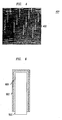
- FIG. 4 shows the illustrative known surface 401 of FIG. 3C with a nanostructure feature pattern of nanoposts 402 disposed on a substrate.
- the surface 401 and the nanoposts 402 of FIG. 4 are, illustratively, made from silicon.
- the nanoposts 402 of FIG. 4 are illustratively approximately 350nm in diameter, approximately 6 ⁇ m high and are spaced approximately 4 ⁇ m apart, center to center. It will be obvious to one skilled in the art that such arrays may be produced with regular spacing or, alternatively, with irregular spacing.
- a “nanostructure” is a predefined structure having at least one dimension of less than one micrometer and a “microstructure” is a predefined structure having at least one dimension of less than one millimeter.
- feature pattern refers to either a pattern of microstructures or a pattern of nanostructures.
- liquid droplet
- liquid droplet are used herein interchangeably. Each of those terms refers to a liquid or a portion of liquid, whether in droplet form or not.
- FIGs. 5A and 5B show one embodiment in accordance with the principles of the present invention where electrowetting is used to control the penetration of a liquid into a nanostructured surface. Electrowetting principles are generally described in U.S. Patent Application Serial No. 10/403159 filed March 31, 2003 and titled "Method And Apparatus For Variably Controlling The Movement Of A Liquid On A Nanostructured Surface," which is hereby incorporated by reference herein in its entirety
- a droplet 501 of conducting liquid (such as an electrolyte solution in a liquid-cell battery) is disposed on nanostructure feature pattern of cylindrical nanoposts 502, as described above, such that the surface tension of the droplet 501 results in the droplet being suspended on the upper portion of the nanoposts 502.
- the droplet only covers surface area f 1 of each nanopost.
- the nanoposts 502 are supported by the surface of a conducting substrate 503.
- Droplet 501 is illustratively electrically connected to substrate 503 via lead 504 having voltage source 505.
- An illustrative nanopost is shown in greater detail in FIG. 6. In that figure, nanopost 502 is electrically insulated from the liquid (501 in FIG.
- material 601 such as an insulating layer of dielectric material.
- the nanopost is further separated from the liquid by a low surface energy material 602, such as a well-known fluoro-polymer.
- a low surface energy material allows one to obtain an appropriate initial contact angle between the liquid and the surface of the nanopost. It will be obvious to one skilled in the art that, instead of using two separate layers of different material, a single layer of material that possesses sufficiently low surface energy and sufficiently high insulating properties could be used.
- FIG. 5B shows that, by applying a low voltage (e.g., 10 - 20 volts) to the conducting droplet of liquid 501, a voltage difference results between the liquid 501 and the nanoposts 502.
- a low voltage e.g. 10 - 20 volts
- the contact angle between the liquid and the surface of the nanopost decreases and, at a sufficiently low contact angle, the droplet 501 moves down in the y-direction along the surface of the nanoposts 502 and penetrates the nanostructure feature pattern until it complete surrounds each of the nanoposts 502 and comes into contact with the upper surface of substrate 503.
- the droplet covers surface area f 2 of each nanopost. Since f 2 » f 1 , the overall contact area between the droplet 501 and the nanoposts 502 is relatively high such that the droplet 501 contacts the substrate 503.
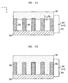
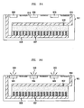
- FIG. 7 shows an illustrative battery 701 in accordance with the principles of the present invention whereby an electrolyte fluid 702 is contained within a housing having containment walls 703.
- the electrolyte fluid 702 is in contact with positive electrode 704, but is separated from negative electrode 708 by nanostructured surface 707.
- Nanostructured surface 707 may be the surface of the negative electrode or, alternatively, may be a surface bonded to the negative electrode.
- the nanostructured surface could also be used in association with the positive electrode with similarly advantageous results.
- the electrolyte fluid is suspended on the tops of the nanoposts of the surface, similar to the droplet of FIG. 5A.
- the battery 701 is inserted, for example, into electrical circuit 705 having load 706.
- FIG. 8 shows the battery 701 of FIG. 7 inserted into electrical circuit 705 wherein, utilizing the electrowetting principles described above, a voltage is passed over the nanostructured surface 707 thus causing the electrolyte fluid 702 to penetrate the surface 707 and to come into contact with the negative electrode 708.
- this voltage can be generated from any number of sources such as, for example, by passing one or more pulses of RF energy through the battery.
- electrons begin flowing in direction 801 along the circuit 705 as described above and the load 706 is powered.
- FIGs. 7 and 8 show how a battery can be stored without depletion for a relatively long period of time and can then be "turned on" at a desired point in time to power one or more electrical loads in an electrical circuit.
- FIGs. 9A and 9B show a cross section of an illustrative use of the battery of FIGs. 7 and 8 in a small electronics package 901.
- package 901 has a battery portion (having a positive electrode 904, negative electrode 908, nanostructured surface 907, and electrolyte fluid 902) electrically connected to an illustrative laser portion (having lasers 906).
- a battery portion having a positive electrode 904, negative electrode 908, nanostructured surface 907, and electrolyte fluid 902
- an illustrative laser portion having lasers 906.
- package 901 may be an integrated device formed entirely from one material, such as a silicon wafer or, alternatively, the battery portion may be formed separately and later connected in the manufacturing process to the laser portion of the package 901.
- 9A and 9B can be illustratively manufactured as a device of any size in any desired geometric shape (e.g., a square, circle, rectangle, etc).
- the package 901 may be manufactured such that surface 910 has a surface area of 1 mm 2 to 100 mm 2 .
- surface 910 has a surface area of 1 mm 2 to 100 mm 2 .
- One skilled in the art will recognize that a variety of shapes having a variety of surface areas will be advantageous in various applications.
- the electrolyte fluid 902 penetrates the surface 907 and contacts electrode 908. Once again, this voltage can be generated by an RF pulse generated external to the battery. Reactions between the electrodes 904 and 908 begin and an electrical current begins flowing along the electrical circuit connecting the battery to the lasers 906. Thus, lasers 906 begin emitting light.
- FIGs. 10A and 10B and 11 show one illustrative use for the electronics package of FIGs. 9A and 9B.
- a container 1001 such as a projectile
- an adhesive liquid 1002 in which a plurality of the electronics packages 901 of FIGs 9A and 9B are disposed.
- the adhesive liquid is illustratively a gel that has a long shelf life (i.e., having a viscosity that will not change over a relatively long period of time) and which functions to maintain a separation distance between the plurality of electronics packages 901.
- the projectile is, illustratively, formed from a polymeric material such as a common PVC or ABS plastic material.
- An illustrative liquid suitable for use in the embodiment of FIGs. 10A and 10B is a soft adhesive in the urethane-based elastomeric adhesive family.
- the battery portions of the electronics packages 901 are not active and the lasers do not emit light, similar to the embodiment of FIG. 9A as described above.
- device 1005 when it is desired that the lasers begin to emit light, device 1005 generates one or more RF energy pulses 1004 that are passed through the container 1001, thus passing a voltage over the nanostructured surfaces 907 of FIG. 9B and causing the electrolyte in the batteries of packages 901 to contact both electrodes 904 and 908 of FIG. 9B. Accordingly, as in the embodiment of FIG.
- lasers 906 begin to emit light.
- device 1005 may be a component of the gun that generates RF pulses to activate the lasers of the packages 901.
- gun is defined as a handgun, a rifle, a cannon, slingshot or any other such device suitable for launching a projectile toward a target.
- any suitable RF energy-generating device may be used to active the lasers of the electronics packages 901.
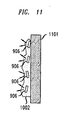
- FIG. 11 shows how, when the projectile 1001 of FIGs. 10A and 10B contacts a surface 1101, illustratively the surface of a vehicle, the projectile breaks apart and the liquid 1002 adheres to the surface1101. Hence, the light emitting packages 901 within the liquid also adhere to the surface 1101 of the vehicle.
- Some military ordinance, particularly bombs and/or missiles dropped from airborne platforms, are adapted to home into laser light of a particular frequency.
- the light-emitting packages 906 can thus be used as a military laser targeting device that these bombs or missiles can home into.
- this form of laser targeting device have advantages over currently-used laser targeting systems.
- one current system relies on manual "painting" of a target with a laser.
- a person on the ground must remain in proximity with the target and shine a laser onto the target, thus placing the person in jeopardy of being discovered or injured.
- Another current system relies on an aircraft to paint the target with the laser. However, this requires the aircraft to once again remain in the proximity of the target until the bomb or missile strikes the target. This is similarly undesirable.
- the projectiles of FIGs. 10A and 10B have the advantage that they can be fired at a vehicle and act as self-generating laser emitters. Thus neither a person nor an aircraft is required to paint the target with a laser. Additionally, one skilled in the art will recognize that the laser emitters of FIGs. 10A and 10B do not have to be activated prior to firing the projectile. Instead, the projectiles may be fired and the inactive emitters attached to a surface 1101, as shown in FIG. 11. Then, at a later time an RF energy pulse can be generated by any suitable source that will activate the laser emitters.
- different laser signals can be emitted by the laser packages in different projectiles, such as by using different encryption of the signals, thus allowing target differentiation by different ordinance.
Landscapes
- Engineering & Computer Science (AREA)
- Chemical & Material Sciences (AREA)
- Chemical Kinetics & Catalysis (AREA)
- Electrochemistry (AREA)
- General Chemical & Material Sciences (AREA)
- Manufacturing & Machinery (AREA)
- General Engineering & Computer Science (AREA)
- Primary Cells (AREA)
- Hybrid Cells (AREA)
- Battery Electrode And Active Subsutance (AREA)
Applications Claiming Priority (2)
| Application Number | Priority Date | Filing Date | Title |
|---|---|---|---|
| US716084 | 2003-11-18 | ||
| US10/716,084 US7227235B2 (en) | 2003-11-18 | 2003-11-18 | Electrowetting battery having a nanostructured electrode surface |
Publications (2)
| Publication Number | Publication Date |
|---|---|
| EP1533857A1 EP1533857A1 (en) | 2005-05-25 |
| EP1533857B1 true EP1533857B1 (en) | 2007-01-03 |
Family
ID=34435731
Family Applications (1)
| Application Number | Title | Priority Date | Filing Date |
|---|---|---|---|
| EP04256701A Expired - Lifetime EP1533857B1 (en) | 2003-11-18 | 2004-10-29 | Electrowetting battery having a nanostructured electrode surface |
Country Status (6)
Families Citing this family (30)
| Publication number | Priority date | Publication date | Assignee | Title |
|---|---|---|---|---|
| US20040191127A1 (en) | 2003-03-31 | 2004-09-30 | Avinoam Kornblit | Method and apparatus for controlling the movement of a liquid on a nanostructured or microstructured surface |
| US8124423B2 (en) | 2003-09-30 | 2012-02-28 | Alcatel Lucent | Method and apparatus for controlling the flow resistance of a fluid on nanostructured or microstructured surfaces |
| US7785733B2 (en) * | 2003-11-18 | 2010-08-31 | Alcatel-Lucent Usa Inc. | Reserve cell-array nanostructured battery |
| US7749646B2 (en) * | 2004-03-18 | 2010-07-06 | Alcatel-Lucent Usa Inc. | Reversibly-activated nanostructured battery |
| US7618746B2 (en) * | 2004-03-18 | 2009-11-17 | Alcatel-Lucent Usa Inc. | Nanostructured battery having end of life cells |
| US7323033B2 (en) * | 2004-04-30 | 2008-01-29 | Lucent Technologies Inc. | Nanostructured surfaces having variable permeability |
| US7608446B2 (en) * | 2004-09-30 | 2009-10-27 | Alcatel-Lucent Usa Inc. | Nanostructured surface for microparticle analysis and manipulation |
| US8734003B2 (en) | 2005-09-15 | 2014-05-27 | Alcatel Lucent | Micro-chemical mixing |
| US8721161B2 (en) | 2005-09-15 | 2014-05-13 | Alcatel Lucent | Fluid oscillations on structured surfaces |
| US7449649B2 (en) * | 2006-05-23 | 2008-11-11 | Lucent Technologies Inc. | Liquid switch |
| KR101310553B1 (ko) * | 2006-09-22 | 2013-09-23 | 주식회사 엘지화학 | 전극과 전해액 간의 젖음성이 향상된 전기화학소자 및 그제조방법 |
| US9021955B2 (en) * | 2007-07-10 | 2015-05-05 | Omnitek Partners Llc | Inertially operated electrical initiation devices |
| US9470497B2 (en) * | 2007-07-10 | 2016-10-18 | Omnitek Partners Llc | Inertially operated piezoelectric energy harvesting electronic circuitry |
| US9097502B2 (en) * | 2007-07-10 | 2015-08-04 | Omnitek Partners Llc | Inertially operated electrical initiation devices |
| US8596198B2 (en) * | 2007-07-10 | 2013-12-03 | Omnitek Partners Llc | Inertially operated electrical initiation methods |
| US10447179B2 (en) * | 2007-07-10 | 2019-10-15 | Omnitek Partners Llc | Inertially operated piezoelectric energy harvesting electronic circuitry |
| US8677900B2 (en) * | 2007-07-10 | 2014-03-25 | Omnitek Partners Llc | Inertially operated electrical initiation devices |
| US9910060B2 (en) * | 2007-07-10 | 2018-03-06 | Omnitek Partners Llc | Piezoelectric-based multiple impact sensors and their electronic circuitry |
| US8042469B2 (en) * | 2007-07-10 | 2011-10-25 | Omnitek Partners Llc | Electrically initiated inertial igniters for thermal batteries and the like |
| US8776688B2 (en) * | 2007-07-10 | 2014-07-15 | Omnitek Partners Llc | Electrically initiated inertial igniters for thermal batteries and the like |
| US9194681B2 (en) * | 2007-07-10 | 2015-11-24 | Omnitek Partners Llc | Inertially operated electrical initiation devices |
| US9587924B2 (en) * | 2007-07-10 | 2017-03-07 | Omnitek Partners Llc | Shock detection circuit and method of shock detection |
| US8601949B2 (en) * | 2007-07-10 | 2013-12-10 | Omnitek Partners Llc | Inertially operated electrical initiation devices |
| US10581347B2 (en) * | 2007-07-10 | 2020-03-03 | Omnitek Partners Llc | Manually operated piezoelectric energy harvesting electronic circuitry |
| US11248893B2 (en) * | 2008-06-29 | 2022-02-15 | Omnitek Partners Llc | Inertially operated piezoelectric energy harvesting electronic circuitry |
| US10598473B2 (en) * | 2008-06-29 | 2020-03-24 | Omnitek Partners Llc | Inertially operated piezoelectric energy harvesting electronic circuitry |
| CN102279519B (zh) * | 2011-07-11 | 2013-01-02 | 西安交通大学 | 一种三维微/纳结构的流体介电泳力扫描压印成形方法 |
| CN107074524B (zh) * | 2014-07-18 | 2020-01-17 | 加利福尼亚大学董事会 | 在浸没的表面上的微特征中保持气体的设备和方法 |
| KR102690251B1 (ko) * | 2018-09-28 | 2024-07-30 | 주식회사 엘지에너지솔루션 | 전기화학소자의 제조방법 |
| JP7313616B2 (ja) * | 2019-01-22 | 2023-07-25 | 国立大学法人東北大学 | 熱電変換装置 |
Family Cites Families (9)
| Publication number | Priority date | Publication date | Assignee | Title |
|---|---|---|---|---|
| FR2548431B1 (fr) | 1983-06-30 | 1985-10-25 | Thomson Csf | Dispositif a commande electrique de deplacement de fluide |
| CA1287072C (en) | 1986-10-03 | 1991-07-30 | Larry D. Brailean | Trackable arrow |
| US5254415A (en) * | 1992-04-09 | 1993-10-19 | Saft America Inc. | Stacked cell array bipolar battery with thermal sprayed container and cell seal |
| WO1998048456A1 (en) | 1997-04-24 | 1998-10-29 | Massachusetts Institute Of Technology | Nanowire arrays |
| US6185961B1 (en) * | 1999-01-27 | 2001-02-13 | The United States Of America As Represented By The Secretary Of The Navy | Nanopost arrays and process for making same |
| AU2002324437A1 (en) | 2001-06-08 | 2002-12-23 | The Penn State Research Foundation | Electronic and opto-electronic devices fabricated from nanostructured high surface to volume ratio thin films |
| JP3662863B2 (ja) * | 2001-07-31 | 2005-06-22 | Necパーソナルプロダクツ株式会社 | 光銃、標的ボックス、射撃ボックス、及び、光銃の射撃システム |
| US6911280B1 (en) * | 2001-12-21 | 2005-06-28 | Polyplus Battery Company | Chemical protection of a lithium surface |
| US7323033B2 (en) * | 2004-04-30 | 2008-01-29 | Lucent Technologies Inc. | Nanostructured surfaces having variable permeability |
-
2003
- 2003-11-18 US US10/716,084 patent/US7227235B2/en not_active Expired - Lifetime
-
2004
- 2004-10-29 DE DE602004004044T patent/DE602004004044T2/de not_active Expired - Lifetime
- 2004-10-29 EP EP04256701A patent/EP1533857B1/en not_active Expired - Lifetime
- 2004-11-17 KR KR1020040093829A patent/KR101107876B1/ko not_active Expired - Fee Related
- 2004-11-17 CN CNB2004100947332A patent/CN100459234C/zh not_active Expired - Fee Related
- 2004-11-18 JP JP2004334091A patent/JP4933727B2/ja not_active Expired - Fee Related
Also Published As
| Publication number | Publication date |
|---|---|
| CN1630120A (zh) | 2005-06-22 |
| DE602004004044D1 (de) | 2007-02-15 |
| JP2005150119A (ja) | 2005-06-09 |
| KR101107876B1 (ko) | 2012-01-30 |
| DE602004004044T2 (de) | 2007-06-28 |
| KR20050048491A (ko) | 2005-05-24 |
| CN100459234C (zh) | 2009-02-04 |
| US7227235B2 (en) | 2007-06-05 |
| EP1533857A1 (en) | 2005-05-25 |
| JP4933727B2 (ja) | 2012-05-16 |
| US20050106459A1 (en) | 2005-05-19 |
Similar Documents
| Publication | Publication Date | Title |
|---|---|---|
| EP1533857B1 (en) | Electrowetting battery having a nanostructured electrode surface | |
| ES2742225T3 (es) | Dispositivo de electrohilado portátil | |
| ES2385803T3 (es) | Dispositivo de pulverización electrostática y procedimiento de pulverización electrostática | |
| US10371493B2 (en) | Target assignment projectile | |
| US20220074715A1 (en) | Polymorphic conducted electrical weapon | |
| KR20080039900A (ko) | 신경근육 파괴에 의해 타깃을 이동 불가능하게 하기 위한비살상 무선 스턴 발사체 시스템 | |
| US10330090B2 (en) | Generating electrospray from a ferrofluid | |
| US7935437B2 (en) | Reversibly-activated nanostructured battery | |
| KR20170028050A (ko) | 박막 형성 장치, 이를 이용한 유기 발광 소자 및 이의 제조 방법 | |
| WO2020023654A1 (en) | Thruster device | |
| US11280591B2 (en) | Intelligent munition | |
| CN108275288B (zh) | 无毒双模式微推进系统及其工作方法 | |
| US11242844B2 (en) | Fiber-fed advanced pulsed plasma thruster (FPPT) | |
| JP2009507170A (ja) | 非対称コンデンサへ制御されたプラズマ環境を導入することにより、指向性のある力を生成するシステム、装置および方法 | |
| US10746515B1 (en) | Tracked synthetic ordnance | |
| US20210078734A1 (en) | Micro-cathode matrix arc thrusters | |
| JPH10302811A (ja) | 注液式電池 | |
| US20100247982A1 (en) | Reserve cell-array nanostructured battery | |
| US9366511B1 (en) | Reduced drag projectile | |
| EP4073461B1 (en) | Primer with voltage polarity immunity using reverse parallel laser diodes | |
| Turchi et al. | Electrostatic acceleration of microprojectiles to ultrahypervelocities | |
| JPH025767A (ja) | 宇宙浮力飛翔体 |
Legal Events
| Date | Code | Title | Description |
|---|---|---|---|
| PUAI | Public reference made under article 153(3) epc to a published international application that has entered the european phase |
Free format text: ORIGINAL CODE: 0009012 |
|
| 17P | Request for examination filed |
Effective date: 20041108 |
|
| AK | Designated contracting states |
Kind code of ref document: A1 Designated state(s): AT BE BG CH CY CZ DE DK EE ES FI FR GB GR HU IE IT LI LU MC NL PL PT RO SE SI SK TR |
|
| AX | Request for extension of the european patent |
Extension state: AL HR LT LV MK |
|
| AKX | Designation fees paid |
Designated state(s): DE FR GB |
|
| GRAP | Despatch of communication of intention to grant a patent |
Free format text: ORIGINAL CODE: EPIDOSNIGR1 |
|
| GRAS | Grant fee paid |
Free format text: ORIGINAL CODE: EPIDOSNIGR3 |
|
| GRAA | (expected) grant |
Free format text: ORIGINAL CODE: 0009210 |
|
| AK | Designated contracting states |
Kind code of ref document: B1 Designated state(s): DE FR GB |
|
| REG | Reference to a national code |
Ref country code: GB Ref legal event code: FG4D |
|
| REF | Corresponds to: |
Ref document number: 602004004044 Country of ref document: DE Date of ref document: 20070215 Kind code of ref document: P |
|
| ET | Fr: translation filed | ||
| PLBE | No opposition filed within time limit |
Free format text: ORIGINAL CODE: 0009261 |
|
| STAA | Information on the status of an ep patent application or granted ep patent |
Free format text: STATUS: NO OPPOSITION FILED WITHIN TIME LIMIT |
|
| 26N | No opposition filed |
Effective date: 20071005 |
|
| REG | Reference to a national code |
Ref country code: GB Ref legal event code: 732E Free format text: REGISTERED BETWEEN 20131031 AND 20131106 |
|
| REG | Reference to a national code |
Ref country code: FR Ref legal event code: CD Owner name: ALCATEL-LUCENT USA INC. Effective date: 20131122 |
|
| REG | Reference to a national code |
Ref country code: FR Ref legal event code: GC Effective date: 20140410 |
|
| REG | Reference to a national code |
Ref country code: FR Ref legal event code: RG Effective date: 20141015 |
|
| REG | Reference to a national code |
Ref country code: FR Ref legal event code: PLFP Year of fee payment: 12 |
|
| REG | Reference to a national code |
Ref country code: FR Ref legal event code: PLFP Year of fee payment: 13 |
|
| REG | Reference to a national code |
Ref country code: FR Ref legal event code: PLFP Year of fee payment: 14 |
|
| REG | Reference to a national code |
Ref country code: FR Ref legal event code: PLFP Year of fee payment: 15 |
|
| PGFP | Annual fee paid to national office [announced via postgrant information from national office to epo] |
Ref country code: FR Payment date: 20200914 Year of fee payment: 17 |
|
| PGFP | Annual fee paid to national office [announced via postgrant information from national office to epo] |
Ref country code: GB Payment date: 20201021 Year of fee payment: 17 Ref country code: DE Payment date: 20201013 Year of fee payment: 17 |
|
| REG | Reference to a national code |
Ref country code: DE Ref legal event code: R119 Ref document number: 602004004044 Country of ref document: DE |
|
| GBPC | Gb: european patent ceased through non-payment of renewal fee |
Effective date: 20211029 |
|
| PG25 | Lapsed in a contracting state [announced via postgrant information from national office to epo] |
Ref country code: GB Free format text: LAPSE BECAUSE OF NON-PAYMENT OF DUE FEES Effective date: 20211029 Ref country code: DE Free format text: LAPSE BECAUSE OF NON-PAYMENT OF DUE FEES Effective date: 20220503 |
|
| PG25 | Lapsed in a contracting state [announced via postgrant information from national office to epo] |
Ref country code: FR Free format text: LAPSE BECAUSE OF NON-PAYMENT OF DUE FEES Effective date: 20211031 |