EP1533845A1 - Semiconductor memory element and its lifetime operation starting device - Google Patents
Semiconductor memory element and its lifetime operation starting device Download PDFInfo
- Publication number
- EP1533845A1 EP1533845A1 EP03730517A EP03730517A EP1533845A1 EP 1533845 A1 EP1533845 A1 EP 1533845A1 EP 03730517 A EP03730517 A EP 03730517A EP 03730517 A EP03730517 A EP 03730517A EP 1533845 A1 EP1533845 A1 EP 1533845A1
- Authority
- EP
- European Patent Office
- Prior art keywords
- semiconductor
- memory element
- semiconductor memory
- circuit portion
- organic semiconductor
- Prior art date
- Legal status (The legal status is an assumption and is not a legal conclusion. Google has not performed a legal analysis and makes no representation as to the accuracy of the status listed.)
- Withdrawn
Links
Images





Classifications
-
- G—PHYSICS
- G11—INFORMATION STORAGE
- G11C—STATIC STORES
- G11C29/00—Checking stores for correct operation ; Subsequent repair; Testing stores during standby or offline operation
- G11C29/04—Detection or location of defective memory elements, e.g. cell constructio details, timing of test signals
- G11C29/50—Marginal testing, e.g. race, voltage or current testing
-
- H—ELECTRICITY
- H10—SEMICONDUCTOR DEVICES; ELECTRIC SOLID-STATE DEVICES NOT OTHERWISE PROVIDED FOR
- H10K—ORGANIC ELECTRIC SOLID-STATE DEVICES
- H10K19/00—Integrated devices, or assemblies of multiple devices, comprising at least one organic element specially adapted for rectifying, amplifying, oscillating or switching, covered by group H10K10/00
-
- H—ELECTRICITY
- H10—SEMICONDUCTOR DEVICES; ELECTRIC SOLID-STATE DEVICES NOT OTHERWISE PROVIDED FOR
- H10K—ORGANIC ELECTRIC SOLID-STATE DEVICES
- H10K19/00—Integrated devices, or assemblies of multiple devices, comprising at least one organic element specially adapted for rectifying, amplifying, oscillating or switching, covered by group H10K10/00
- H10K19/10—Integrated devices, or assemblies of multiple devices, comprising at least one organic element specially adapted for rectifying, amplifying, oscillating or switching, covered by group H10K10/00 comprising field-effect transistors
-
- H—ELECTRICITY
- H10—SEMICONDUCTOR DEVICES; ELECTRIC SOLID-STATE DEVICES NOT OTHERWISE PROVIDED FOR
- H10W—GENERIC PACKAGES, INTERCONNECTIONS, CONNECTORS OR OTHER CONSTRUCTIONAL DETAILS OF DEVICES COVERED BY CLASS H10
- H10W42/00—Arrangements for protection of devices
- H10W42/40—Arrangements for protection of devices protecting against tampering, e.g. unauthorised inspection or reverse engineering
-
- H—ELECTRICITY
- H10—SEMICONDUCTOR DEVICES; ELECTRIC SOLID-STATE DEVICES NOT OTHERWISE PROVIDED FOR
- H10K—ORGANIC ELECTRIC SOLID-STATE DEVICES
- H10K10/00—Organic devices specially adapted for rectifying, amplifying, oscillating or switching; Organic capacitors or resistors having potential barriers
- H10K10/80—Constructional details
- H10K10/88—Passivation; Containers; Encapsulations
-
- H—ELECTRICITY
- H10—SEMICONDUCTOR DEVICES; ELECTRIC SOLID-STATE DEVICES NOT OTHERWISE PROVIDED FOR
- H10K—ORGANIC ELECTRIC SOLID-STATE DEVICES
- H10K19/00—Integrated devices, or assemblies of multiple devices, comprising at least one organic element specially adapted for rectifying, amplifying, oscillating or switching, covered by group H10K10/00
- H10K19/80—Interconnections, e.g. terminals
-
- H—ELECTRICITY
- H10—SEMICONDUCTOR DEVICES; ELECTRIC SOLID-STATE DEVICES NOT OTHERWISE PROVIDED FOR
- H10W—GENERIC PACKAGES, INTERCONNECTIONS, CONNECTORS OR OTHER CONSTRUCTIONAL DETAILS OF DEVICES COVERED BY CLASS H10
- H10W42/00—Arrangements for protection of devices
-
- Y—GENERAL TAGGING OF NEW TECHNOLOGICAL DEVELOPMENTS; GENERAL TAGGING OF CROSS-SECTIONAL TECHNOLOGIES SPANNING OVER SEVERAL SECTIONS OF THE IPC; TECHNICAL SUBJECTS COVERED BY FORMER USPC CROSS-REFERENCE ART COLLECTIONS [XRACs] AND DIGESTS
- Y10—TECHNICAL SUBJECTS COVERED BY FORMER USPC
- Y10S—TECHNICAL SUBJECTS COVERED BY FORMER USPC CROSS-REFERENCE ART COLLECTIONS [XRACs] AND DIGESTS
- Y10S257/00—Active solid-state devices, e.g. transistors, solid-state diodes
- Y10S257/922—Active solid-state devices, e.g. transistors, solid-state diodes with means to prevent inspection of or tampering with an integrated circuit, e.g. "smart card", anti-tamper
Definitions
- the present invention relates to a semiconductor memory element using an organic semiconductor having a predetermined lifetime for defining a retention time during which recorded data can be reproduced and capable of starting the lifetime at a predetermined time, and further relates to a lifetime operation starting apparatus therefor.
- High density and high integration semiconductor devices have been manufactured and supplied, owing to a development of fine technology in a semiconductor manufacturing.
- a semiconductor memory manufactured in a sub micron rule a great number of memory elements are formed in one chip, which allows recording music and video for a long time, coupled with a lowered bit unit price and with a development in data compressing technology.
- employing an organic semiconductor element with a lower price may make the bit unit price lower.
- the semiconductor memory useful as a record medium as well as in view of the cost, it is expected to prevent or block the data reading after a predetermined time elapse from the data recording, for example in an application for a commuter pass (ticket), or an application in a rental business of music or video soft and the like.
- a predetermined time elapse from the data recording for example in an application for a commuter pass (ticket), or an application in a rental business of music or video soft and the like.
- a gate insulation layer may be formed of a first layer of a silicon dioxide film, a second layer of a silicon nitride film and a third layer of a silicon dioxide film, in which a composition rate of Si atom and N atom in the second layer of the silicon nitride film is set to a value corresponding to a desired data effective time.
- the data effective time is expected to be set in such a manner that a shallow electric charge lap is positively formed to deteriorate the memory retention, and an amount of the electric charge to be accumulated in an electric charge accumulation mechanism is reduced and thereby the lifetime of the data retention is shortened.
- the lifetime of record data in this type of memory is determined by controlling the composition rate of Si atom and N atom in the silicon nitride during the chip fabrication.
- the lifetime of the record data is determined by controlling the composition rate of Si atom to N atom
- the memory lifetime is adversely determined on the fabrication.
- the lifetime is based on the fabrication time, and it is difficult to know, on an actual data recording, an elapsed time from the fabrication. Therefore, it is not possible to know the effective time from the data recording, which is a problem in a practical use.
- the first semiconductor memory element of the present invention in order to solve the above problems is a semiconductor memory element comprising: a substrate; a semiconductor circuit portion made of an organic semiconductor disposed on the substrate; and a protection portion disposed adjacent to the semiconductor circuit portion, the protection portion being made of a material capable of causing a crack extending to the semiconductor circuit portion due to a predetermined means.
- the semiconductor circuit is made of the organic semiconductor, and the protection portion for protecting a layer forming the semiconductor circuit is disposed.
- the protection portion can make a crack reachable to the layer forming the semiconductor circuit by the predetermined means. From the crack, moisture or oxygen in the air penetrates into the semiconductor circuit portion and diffuses therein. The organic semiconductor is deteriorated in its performance by the moisture or oxygen. And the organic semiconductor fails to function after a certain time period.
- the lifetime in the present invention means a time period from a start time of the deterioration in the organic semiconductor by the performance deterioration material until the organic semiconductor loses the semiconductor function.
- the lifetime can be set depending on the extent of cracks to be caused.
- the second semiconductor memory element of the present invention in order to solve the above problems is a semiconductor memory element comprising: a substrate; a semiconductor circuit portion made of an organic semiconductor disposed on the substrate; a protection portion disposed adjacent to the semiconductor circuit portion and having a window portion; and a freely strippable seal member for sealing the window portion of the protection portion.
- the semiconductor circuit is made of the organic semiconductor, and the protection portion for protecting a layer forming the semiconductor circuit is disposed.
- the protection portion has a window portion, which is sealed with the seal member. If the seal member is stripped off, moisture or oxygen in the air penetrates into the semiconductor circuit and diffuses therein. From then, the organic semiconductor is deteriorated in its performance by the moisture or oxygen. And the organic semiconductor fails to function after a certain time period. Therefore, the memory and the like having the predetermined lifetime are formed.
- the third semiconductor memory element of the present invention in order to solve the above problems is a semiconductor memory element comprising: a substrate; a semiconductor circuit portion made of an organic semiconductor disposed on the substrate; a protection portion disposed adjacent to the semiconductor circuit portion; and a performance deterioration material layer including a performance deterioration material and disposed adjacent to the protection portion, the protection portion being made of a material capable of causing a crack extending to the semiconductor circuit portion due to a predetermined means.
- the semiconductor circuit is made of the organic semiconductor, and the protection portion for protecting a layer forming the semiconductor circuit is disposed. Furthermore, the performance deterioration material layer including the performance deterioration material for deteriorating the organic semiconductor material is disposed above the protection portion.
- the protection portion can make a crack reachable to the layer forming the semiconductor circuit by the predetermined means. From the crack, the performance deterioration material in the performance deterioration material layer penetrates into the semiconductor circuit portion and diffuses therein.
- the organic semiconductor is deteriorated in its performance by the performance deterioration material. And the organic semiconductor fails to function after a certain time period. Therefore, the memory and the like having the predetermined lifetime to make the recorded data reproduction impossible after a certain time period is formed. Furthermore, the lifetime can be set depending on the extent of cracks to be caused.
- the predetermined means is a mechanical punch means.
- a micro-hole / micro-holes is/are formed in the protection portion by a mechanical means such as a needle like means.
- the moisture or oxygen in the air, or the performance deterioration material in the performance deterioration material layer can penetrate into the semiconductor circuit portion and diffuse therein.
- the predetermined means is a heating means.
- the crack is caused by heating the protection portion.
- the moisture or oxygen in the air, or the performance deterioration material in the performance deterioration material layer can penetrate into the semiconductor circuit portion and diffuse therein.
- the predetermined means is a pressurizing means.
- the crack is caused by pressurizing the protection portion.
- the moisture or oxygen in the air, or the performance deterioration material in the performance deterioration material layer can penetrate into the semiconductor circuit portion and diffuse therein.
- the predetermined means is a light irradiation means.
- the crack is caused by irradiating light of a predetermined wavelength to the protection portion.
- the moisture or oxygen in the air, or the performance deterioration material in the performance deterioration material layer can penetrate into the semiconductor circuit portion and diffuse therein.
- the fourth semiconductor memory element of the present invention in order to solve the above problems is a semiconductor memory element comprising: a substrate; a semiconductor circuit portion disposed on the substrate and made of an organic semiconductor including a performance deterioration material; and a protection portion disposed adjacent to the semiconductor circuit portion, wherein the performance deterioration material is activated by a predetermined means.
- the semiconductor circuit is made of the organic semiconductor, and the protection portion for protecting a layer forming the semiconductor circuit is disposed.
- the performance deterioration material for deteriorating the organic semiconductor performance is dispersed in the semiconductor circuit portion.
- the deterioration material is activated by releasing the trigger ("releasing the trigger" in the present application means to start the activation of the performance deterioration material), which causes the deterioration of the organic semiconductor.
- the organic semiconductor fails to function after a certain time period. Therefore, the memory and the like having the predetermined lifetime to make the recorded data reproduction impossible after a certain time period is formed. Furthermore, the lifetime can be set depending on the extent of the performance deterioration material dispersion or the extent of the activation.
- the fifth semiconductor memory element of the present invention in order to solve the above problems is a semiconductor memory element comprising: a substrate; a semiconductor circuit portion disposed on the substrate and made of an organic semiconductor including a performance deterioration material; and a film disposed adjacent to the semiconductor circuit portion, capable of obtaining light transmissive property due to an irradiation of light having a predetermined wavelength thereon, wherein the performance deterioration material is activated by a predetermined means.
- the semiconductor circuit is made of the organic semiconductor, and the color film layer is disposed above a layer forming the semiconductor circuit to cover and protect the latter.
- the performance deterioration material for deteriorating the organic semiconductor is dispersed in the semiconductor circuit portion.
- the color film obtains light transmissive property by irradiating the light of the predetermined wavelength. Then, the performance deterioration material is activated by the released trigger, and thereby the organic semiconductor is deteriorated. and the organic semiconductor fails to function after a certain time period. Therefore, the memory and the like having the predetermined lifetime to make the recorded data reproduction impossible after a certain time period is formed. Furthermore, the lifetime can be set depending on the extent of the performance deterioration material dispersion or the extent of the activation.
- the sixth semiconductor memory element of the present invention in order to solve the above problems is a semiconductor memory element comprising: a substrate; a semiconductor circuit portion disposed on the substrate and made of an organic semiconductor including a performance deterioration material; a protection portion disposed adjacent to the semiconductor circuit portion and having a window portion; and a freely strippable seal member for sealing the window portion of the protection portion.
- the semiconductor circuit is made of the organic semiconductor, and the protection portion is disposed above a layer forming the semiconductor circuit.
- the performance deterioration material for deteriorating the organic semiconductor is dispersed in the semiconductor circuit portion.
- the protection portion is provided with the window portion at a position corresponding to the semiconductor circuit.
- the window portion is sealed with the seal member. If the seal member is stripped off to release the trigger for activating the performance deterioration material dispersed in the semiconductor circuit portion by the predetermined means, the organic semiconductor is deteriorated. And the organic semiconductor fails to function after a certain time period. Therefore, the memory and the like having the predetermined lifetime to make the recorded data reproduction impossible after a certain time period is formed. Furthermore, the lifetime can be set depending on the extent of the performance deterioration material dispersion or the extent of the activation.
- the performance deterioration material is encapsulated.
- some performance deterioration materials begin to deteriorate from the beginning of the dispersion. However, if these performance deterioration materials are encapsulated and the capsule is broken on the time to begin the deterioration, the organic semiconductor starts to deteriorate.
- the predetermined means is a pressurizing means.
- the performance deterioration material dispersed in the semiconductor circuit portion made of the organic semiconductor is activated by pressurizing.
- the predetermined means is a heating means.
- the performance deterioration material dispersed in the semiconductor circuit portion made of the organic semiconductor is activated by heating.
- the predetermined means is an UV irradiation means.
- the performance deterioration material dispersed in the semiconductor circuit portion made of the organic semiconductor is activated by irradiating UV (ultraviolet) rays.
- the predetermined means is an electron beam irradiation means.
- the performance deterioration material dispersed in the semiconductor circuit portion made of the organic semiconductor is activated by irradiating electron beam.
- the deterioration in the semiconductor circuit portion of the organic semiconductor is started by stripping off the seal member.
- the protection portion provided with the window portion corresponding to a predetermined circuit position of the semiconductor circuit portion is provided, if the seal member sealing the window portion is stripped off, the organic semiconductor starts to deteriorate.
- the semiconductor portion is a semiconductor portion in a range corresponding to a predetermined circuit portion of the semiconductor circuit portion.
- the organic semiconductor in the semiconductor circuit portion to be deteriorated, the organic semiconductor can be deteriorated relative to an arbitrary part. Therefore, there is no need of the configuration to deteriorate the organic semiconductor relative to the entire circuit.
- the predetermined circuit portion is a data area.
- the lifetime is determined by deteriorating the data area of the semiconductor circuit.
- the predetermined circuit portion is a management information area.
- the lifetime is determined by deteriorating the management information area of the semiconductor circuit.
- the predetermined circuit portion is an electric power shutdown switch.
- the lifetime is determined by deteriorating the electric power source shut down switch of the semiconductor circuit.
- the predetermined circuit portion is an encryption key record area.
- the lifetime is determined by deteriorating the encryption key record area of the semiconductor circuit.
- the first lifetime operation starting apparatus for the semiconductor memory element of the present invention in order to solve the above problems is a lifetime operation starting apparatus having an starting device for starting an operation of a semiconductor memory element using an organic semiconductor within a lifetime, comprising a seal strip off device for stripping off a seal attached to a position corresponding to a predetermined portion of the organic semiconductor in order to deteriorate a performance of the organic semiconductor as the starting device.
- the lifetime operation starting apparatus for the semiconductor memory element of the present invention, in the case that the protection portion covering the organic semiconductor is provided with the window portion, which is sealed with the seal member, the trigger to start the lifetime is stripping off the seal member. Therefore, the lifetime operation starting apparatus is provided with the seal strip off device for stripping off the seal member. A mechanism may be additionally employed in order to strip off the seal automatically, when the semiconductor memory element is mounted onto the record apparatus for the data recording.
- the second lifetime operation starting apparatus for the semiconductor memory element of the present invention a lifetime operation starting apparatus having an starting device for starting an operation of a semiconductor memory element using an organic semiconductor within a lifetime, comprising, in order to cause a crack in a protection portion protecting the organic semiconductor as the starting device, at least one of a mechanical punch device for punching a microhole through the protection portion; a heating device for heating the protection portion; a pressurizing device for pressurizing the protection portion; and a light irradiation device for irradiating the protection portion with light.
- the second lifetime operation starting apparatus for the semiconductor memory element of the present invention there is provided with any one or a plurality of a mechanism for mechanically forming a mirco-hole / micro-holes, a mechanism for causing the crack by heating, a mechanism for causing the crack by pressurizing and a mechanism for causing the crack by irradiation with light, as a device for causing the crack in the protection portion protecting the organic semiconductor and releasing the trigger to the deterioration of the organic semiconductor. It may be employed depending on the formation of the protection portion and the formation of the performance deterioration material. Alternatively, the deterioration speed of the organic semiconductor can be controlled to determine the lifetime by employing a mechanism for controlling the operation time. Furthermore, these mechanisms can be additionally disposed at the record apparatus for the semiconductor memory element, in order to release the trigger on the data recording.
- the third lifetime operation starting apparatus for the semiconductor memory element of the present invention in order to solve the above problems is a lifetime operation starting apparatus having an starting device for starting an operation of a semiconductor memory element using an organic semiconductor within a lifetime, comprising, in order to activate a performance deterioration material dispersed in the organic semiconductor as the starting device, at least one of: a UV irradiation device for irradiating the performance deterioration material in the organic semiconductor with UV rays; and an electron beam irradiation device for irradiating the performance deterioration material in the organic semiconductor with electron beam.
- the third lifetime operation starting apparatus for the semiconductor memory element of the present invention there is provided with any one or a plurality of a mechanism for irradiating the UV rays to the performance deterioration material and a mechanism for irradiating the electron beam to the performance deterioration material, in order to activate the performance deterioration material dispersed in the organic semiconductor. It may be employed depending on the formation of the protection portion and the formation of the performance deterioration material. Furthermore, the deterioration speed of the organic semiconductor can be controlled to determine the lifetime by employing a mechanism for controlling the operation time. Furthermore, these mechanisms can be additionally disposed at the record apparatus for the semiconductor memory element to release the trigger on the data recording.
- the semiconductor memory element according to the present invention is a memory using the organic semiconductor to construct the circuit, allowing the recorded data reading for a certain time period (referred to as the "lifetime" herein as appropriate) during which the memory function is maintained, although the deterioration trigger is released, owing to the organic semiconductor characteristic property, for example the property of the deterioration because of chemical reactions with the moisture or oxygen, or the predetermined chemicals.
- the lifetime of the memory can be activated at any time, and the lifetime length can be set depending on the conditions.
- the element can be in a large size by using a printing technology, and the cost is small.
- the form to make the data reproduction impossible is not limited to delete the recorded data itself, but includes breaking the management information or the encryption key to make a state that the recorded data cannot be reproduced.
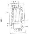
- FIG. 1 illustrates an outline of a semiconductor memory element construction according to the present invention.
- FIG. 2 illustrates an outline of another semiconductor memory element construction according to the present invention.
- FIG. 3 illustrates an outline of a conventional semiconductor memory element for a comparison.
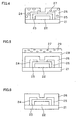
- FIG. 4 illustrates the first element configuration of the semiconductor memory element according to the present invention
- FIG. 5 illustrates the second element configuration.
- FIG. 6 illustrates a conventional element configuration for a comparison.
- the memory 1 of the semiconductor memory element according to the present invention is provided with an address control portion 10; a protection film 11; a performance deterioration material layer 12; data storage areas 14, 15, 16, 17; and a bonding pad 18.
- the address control portion 10 designates storage positions in the data storage areas 14, 15, 16 and 17, on the basis of the addresses of rows and columns inputted from the external terminal.
- the protection film 11 is formed to protect the organic semiconductor layer constructing the semiconductor circuit, and prevents the moisture in the air, the chemicals, the light or the like from penetrating into the organic semiconductor layer. On the other hand, if this protection film 11 is destroyed and the predetermined means are performed, the organic semiconductor layer starts to deteriorate and enters the lifetime length operation.
- the performance deterioration material layer 12 includes the material for deteriorating the organic semiconductor performance. If this material diffuses within the organic semiconductor layer, the organic semiconductor layer is deteriorated to determine the lifetime. Before the diffusion, the protection film 11 prevents the material from contacting with the organic semiconductor layer. As mentioned above, if this protection film 11 is destroyed, the performance deterioration material diffuses within the organic semiconductor layer.
- a method or configuration for deteriorating the organic semiconductor layer is not limited to this example, and various forms will be explained in detail later.
- the data storage areas 14, 15, 16 and 17 are areas for storing data.
- the data effective time can be set for each area. It will be obvious to those skilled in the art that the data storage areas may be a united single area, or may be further divided into more areas. Furthermore, the protection film 11 may be disposed separately and individually for each data storage area. Thereby, it is possible to set individual lifetimes for each data storage area.
- the bonding pad 18 is a connecting terminal for establishing an electrical connection with the external circuit. There are provided with terminals corresponding to an electric power source, a data I/O (input/output), a data address, a record reproduction signal and other control signals of the memory 1.
- the memory 2 of the semiconductor memory element according to the present invention is provided with an address control portion 10; a protection film 11; a performance deterioration material layer 12; a power supply switch 13; data storage areas 14, 15, 16; a bonding pad 18; an encryption key storage area 19; and an encryption circuit 20.
- the constructions and operations of the address control portion 10, the protection film 11, the performance deterioration material layer 12, the data storage areas 14, 15, 16 and the bonding pad 18 are the same as those of the aforementioned memory 1, and thus the same explanation is not repeated.
- the memory 2 is provided with the device for encrypting the data to be recorded, the device for storing the encryption key, and the switch for controlling the power supply respectively to each data storage area and the encryption key storage area.
- the data reproduction operation within the lifetime can be set by deteriorating the organic semiconductor forming the encryption key storage area 19 and the power supply switch 13.
- the power supply switch 13 may be individually provided for each data storage area 14, 15 or 16, and the encryption key storage area 19.
- the protection film 11 is provided above these power supply switches 13, and the performance deterioration material layer 12 is further provided adjacent to the protection film 11. if the protection film 11 above the power supply switch 13 corresponding to a desired area is destroyed, the performance deterioration material in the performance deterioration material layer 12 diffuses within the organic semiconductor forming the desired power supply switch 13, so that the operation of the power supply switch 13 ends with the predetermined lifetime. As the result, the data in the area corresponding to the power supply switch 13 becomes impossible to be read. In the case of a volatile memory, the data is also deleted.
- the encryption key storage area 19 is an area for storing the encryption key to encrypt the data to be recorded.
- the encryption key is used also in the case of decoding the encrypted data.
- the encryption circuit 20 is a circuit for encrypting the data to be recorded on the basis of the encryption key. Furthermore, it may include a circuit for decoding the data for the reproduction, or may read the encrypted data and the encryption key and perform the decoding at the external device such as a personal computer.
- the performance deterioration material layer 12 may be dispersed within the organic semiconductor to activate the performance deterioration material by the predetermined method.
- FIG. 3 illustrates the construction of the conventional memory 3 for a comparison with the memories 1 and 2 of the present invention. There is not provided with the protection film 11 and the performance deterioration material layer 12. There is no technical concept about the memory lifetime, i.e. the reproduction effective time of the recorded data.
- FIG. 4 illustrates the first element structure in which a gate 22, an insulator 23, a source 24 and a drain 25 area disposed on a substrate 21
- a semiconductor layer of an organic semiconductor 26 is further disposed outside of a gate 22, an insulator 23, a source 24 and a drain 25.
- a performance deterioration material 27 is dispersed within the organic semiconductor 26. Some performance deterioration materials 27 are directly dispersed and other performance deterioration materials 27 are encapsulated to be dispersed, depending on the activation form of the performance deterioration material. If the performance deterioration material 27 activates within the organic semiconductor 26, the organic semiconductor 26 starts to deteriorate. And it fails to function as a memory after a predetermined time period.
- the second element structure includes, as shown in FIG. 5, the gate 22, the insulator 23, the source 24 and the drain 25 on the substrate 21, and further includes the semiconductor layer of the organic semiconductor 26 outside of gate 22, the insulator 23, the source 24 and the drain 25. Furthermore, the second element structure includes a protection portion 28 outside of the organic semiconductor 26 on the substrate, and a performance deterioration material layer 29 above the protection portion 28. The performance deterioration material layer 29 includes therein the performance deterioration material 27. If the protection portion 28 is destroyed, the performance deterioration material 27 diffuses within the organic semiconductor 26, so that the organic semiconductor 26 starts to deteriorate until it fails to function as a memory after a predetermined time period.
- FIG. 6 illustrates the conventional element structure in which the gate 22, the insulator 23, the source 24 and the drain 25 are disposed on the substrate 21, and the organic semiconductor 26 is disposed outside of the gate 22, the insulator 23, the source 24 and the drain 25.
- this conventional structure as it is, can be covered by the protection film or the like to prevent the organic semiconductor 26 from contacting with the air. Then, the protection film can be destroyed to cause the operation within the lifetime.
- the conventional element structure can be directly used, without a special treatment of the element structure itself.
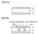
- an organic semiconductor circuit portion 31 and a protection film 32 adjacent to the circuit portion 31 are disposed on the substrate 21.
- heat, pressure, light or the like is applied or irradiated on the protection film 32 to make cracks 32a in the protection film 32.
- the moisture or oxygen in the air penetrates into the organic semiconductor circuit portion 31 and diffuses therein, which deteriorates the function of the organic semiconductor circuit portion 31. Because the deterioration in the function of the organic semiconductor circuit portion 31 progresses, the reproduction of the recorded data becomes impossible after a predetermined time period.
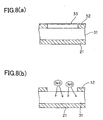
- the organic semiconductor circuit portion 31 and the protection film 32 adjacent to the circuit portion 31 are disposed on the substrate 21.
- the protection film 32 has an opening portion at a predetermined portion of the organic semiconductor circuit portion 31.
- a seal 33 is hermetically disposed above the opening portion. As shown in FIG. 8B, if the seal 33 is stripped off, the moisture or oxygen in the air penetrates into the organic semiconductor circuit portion 31 and diffuses therein to cause the deterioration in the function of the organic semiconductor circuit portion 31. Because the deterioration in the function of the organic semiconductor circuit portion 31 progresses, the data reproduction becomes impossible after a predetermined time period.
- the organic semiconductor circuit portion 31, the protection film 32 adjacent to the circuit portion 31 and the performance deterioration material layer 29 including the performance deterioration material 27 and adjacent to the protection film 32 are disposed on the substrate 21.
- heat, pressure, light or the like is applied or irradiated on the protection film 32 to make cracks 32a in the protection film 32.
- the performance deterioration material 27 in the performance deterioration material layer 29 penetrates into the organic semiconductor circuit portion 31 and diffuses therein to cause the deterioration in the function of the organic semiconductor circuit portion 31. Because the deterioration in the function of the organic semiconductor circuit portion 31 progresses, the reproduction of the recorded data becomes impossible after a predetermined time period.
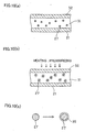
- the organic semiconductor circuit portion 31 and the protection film 32 adjacent to the circuit portion 31 are disposed on the substrate 21. Furthermore, the performance deterioration material 27 is dispersed in the organic semiconductor circuit portion 31. As shown in FIG. 10B, if the performance deterioration material 27 is activated by heating, pressurizing, irradiation with light, and the like, from the top of the protection film 32, the function of the organic semiconductor circuit portion 31 deteriorates. Because the deterioration in the function of the organic semiconductor circuit portion 31 progresses, the reproduction of the recorded data becomes impossible after a predetermined time period.
- this material 27 may be encapsulated into a microcapsule 35, which may be destroyed on the use.
- the introduction of the microcapsule 35 will be explained in detail below.
- time material (corresponds to the performance deterioration material herein) and the activation of the time material will be explained.
- the time material is preliminarily mixed in a cell constructing the organic semiconductor, and this time material is activated by releasing a predetermined trigger, so that the organic semiconductor is deteriorated due to the activated species in order to intentionally obtain the limited lifetime.
- the trigger may be sensing pressure, heat, light or the like.
- time materials tend to start the deterioration without the special treatment if they are mixed in the organic semiconductor.
- Other time materials do not act on the organic semiconductor until the trigger is released.
- An example of the former type (time materials tending to start the deterioration without the special treatment) is benzoyl peroxides or a so-called photopolymerization initiator having ketone group or azo group, from which radicals are caused by UV radiation, encapsulated in microcapsules made of gelatins, formaldehyde resins or polyurethane resins.
- the encapsulated chemicals exit from the microcapsules by means of the trigger and activated by UV radiation.
- the moisture may be encapsulated in the microcapsules so that the organic semiconductor is deteriorated by the moisture emitted from the microcapsules.
- Azo compounds may be encapsulated in the microcapsules so that azo compounds dissolve by heating and cause generation of nitrogen or nitrogen oxides in a form of gas and thereby physically cause cracks in the organic semiconductor layer for the deterioration thereof.
- cyanine dye such as cyanines, isocyanines or pseudocyanines having a heterocycle such as quinolines, thiazoles, pyridines, benzooxazoles or benzothiazoles.
- the performance deterioration material may be used as it is or may be used as encapsulated in the microcapsule, depending on the type of the performance deterioration material.
- the aforementioned treatment depending on the type of the performance deterioration material is employed as well.
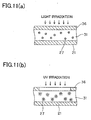
- the organic semiconductor circuit portion 31 and a color film layer 36 adjacent to the circuit portion 31 are disposed on the substrate 21. Furthermore, the performance deterioration material 27 is dispersed in the organic semiconductor circuit portion 31. The light of a predetermined wavelength is irradiated onto the color film layer 36 from the top so that the irradiated portion of the color film layer 36 obtains the light transmissive property in a wide range. Next, as shown in FIG. 11B, UV rays is irradiated to activate the performance deterioration material 27 so that the function of the organic semiconductor circuit portion 31 deteriorates. Because the deterioration in the function of the organic semiconductor circuit portion 31 progresses, the data reproduction becomes impossible after a predetermined time period.
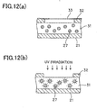
- the organic semiconductor circuit portion 31 and the protection film 32 adjacent to the circuit portion 31 are disposed on the substrate 21. Furthermore, the performance deterioration material 27 is dispersed in the organic semiconductor circuit portion 31.
- the protection film 32 has the opening portion at a position corresponding to a predetermined portion of the organic semiconductor circuit portion 31. The opening portion is sealed with the seal 33.
- FIG. 12B after stripping off the seal 33, UV rays is irradiated to activate the performance deterioration material 27 and thereby deteriorate the function of the organic semiconductor circuit 31. Because the deterioration in the function of the organic semiconductor circuit portion 31 progresses, the data reproduction becomes impossible after a predetermined time period.
- the opening portion may be full-filled by a transparent material.
- the organic semiconductor can be fabricated by using the printing technology, which makes it possible to fabricate a relatively large size memory such as a card-like memory at a low cost.
- a semiconductor chip 43 is enclosed in a card-like package 41, at one edge of which electrodes 42 are formed to electrically contact with an external device.
- the bonding pads 18 of the memory 1 shown in FIG. 1 for example may be connected to electrodes 42, so that an electrical connection between the semiconductor chip 43 and the external device is established.
- the semiconductor chip 43 used for the memory card 5 is the organic semiconductor in a form shown in figs. 7A-7B, or shown in figs. 10A-10C.
- the crack 32a is caused in the protection layer by heating or pressurizing or irradiation with light from the top of the semiconductor chip 43, so that the moisture or oxygen in the air diffuses in the semiconductor circuit portion 31 made of the organic semiconductor and thereby the deterioration in the organic semiconductor progress.
- the data reproduction is performable within the lifetime.
- the semiconductor chip 43 is enclosed in the card-like package 41, at one edge of which electrodes 42 are formed to contact with the external device.
- the bonding pads 18 of the memory 1 shown in FIG. 1 are connected to the electrodes 42 to establish the electrical connection between the semiconductor chip 43 and the external device.
- the top portion of the semiconductor 43 is covered with the color film layer 36.
- the semiconductor chip 43 used for the memory card 36 is the organic semiconductor in a form shown in figs. 11A-11B.
- the light of the predetermined wavelength is irradiated onto the color film layer 36, and then UV rays is irradiated to activate the performance deterioration material 27 dispersed in the semiconductor circuit portion 31, so that the deterioration in the organic semiconductor progresses and allows the record data reproduction within the lifetime.
- the semiconductor chip 43 is enclosed in the card-like package 41, at one edge of which electrodes 42 are formed to contact with the external device.
- the bonding pads 18 of the memory 1 shown in FIG. 1 may be connected to the electrodes 42 to establish the electrical connection between the semiconductor chip 43 and the external device.
- the semiconductor chip 43 has the opening portion at the top portion thereof, which is sealed with the seal 33.
- An ear portion 33a is formed at the tip of the seal 33 to facilitate the stripping.
- the semiconductor chip 43 used for the memory card 7 is the organic semiconductor in a form shown in figs. 8A-8B, or shown in figs. 12A-12B.
- the organic semiconductor shown in figs. 8A-8B if the seal 33 is stripped off, the moisture or oxygen in the air diffuses in the semiconductor circuit portion 31, so that the deterioration in the organic semiconductor progresses and the data reproduction is allowed within the lifetime.
- the opening portion may be covered with a light transmissive material. It is particularly effective in a form in which the deterioration speed and thereby the lifetime are controlled by UV irradiation amount.
- a card form can be off course made from the organic semiconductor shown in figs. 9A-9B.
- the crack 32a is caused in the protection film 32 by heating or pressurizing, or irradiation with light and so on, so that the performance deterioration material 27 in the performance deterioration material layer 29 diffuses in the semiconductor circuit portion 31 and thereby the deterioration in the organic semiconductor progresses, and the record data reproduction is allowed within the lifetime.
- This example is a device for releasing the trigger to start the lifetime of the aforementioned memory card, and for recording and reproducing the data.
- the lifetime operation starting apparatus 8 is used for the organic semiconductor optically causing the performance deterioration as shown in figs. 7A-7B, figs. 9A-9B, or figs. 11A-11B. It is provided with a handling portion 51; a light source 52; an electrode 53; a control portion 54; a light source drive portion 55; a data record and reproduction portion 56, as shown in FIG. 16.
- the operation portion 51 is for inputting an operational command to the lifetime operation starting apparatus 8.
- the light source 52 is for irradiating the light onto the semiconductor chip 43 of the memory card 6 to diffuse the performance deterioration material 27 in the organic semiconductor portion or activate the performance deterioration material 27.
- the electrode 53 contacts with the electrode 42 of the memory card 6 to supply the electrical power, input or output the record/reproduction control signal or the data.
- the control portion 54 is for controlling the entire operation of the apparatus.
- the light source drive portion 55 is for turning on the light source 52 under a control of the control portion 54.
- the data record and reproduction portion 56 is for writing (recording) the data on to the memory card 6 or reading (reproducing) the data.
- the multipurpose function for the apparatus such as display function, is employed.
- the deterioration of the memory card 6 is started by the irradiation with light from the light source 52, allowing the data reproduction within the lifetime.
- the irradiation time of the light can be controlled depending on the rental fee when the data is recorded, so that the lifetime can be set.
- the invention is not limited to the aforementioned structure, and the seal strip structure is provided in the case of the memory card in a form sealed with the seal as shown in figs. 8A-8B or figs. 12A-12B, or the heating means or pressure means is provided in the case of the memory card in a form involving the heat or pressure application as shown in figs. 10A-10C.
- the reproduction time of the recorded data i.e. the start time of the reproducible lifetime can be freely set. Furthermore, the lifetime itself can be freely set. Furthermore, since the semiconductor memory element is made of the organic semiconductor, the semiconductor memory element suitable for the mass production at a low cost is presented.
- the semiconductor memory element and the lifetime operation starting apparatus therefor are applicable to various memory elements and various record devices for recording at high density and reproducing a large amount of information including various contents information such as video information or audio information, various data information for computers, or control information, by means of the organic semiconductor available at a relatively low cost and suitable for downsizing in its scale or thickness.
Landscapes
- Semiconductor Memories (AREA)
- Storage Device Security (AREA)
- Thin Film Transistor (AREA)
Abstract
Description
Claims (30)
- A semiconductor memory element comprising:a substrate;a semiconductor circuit portion made of an organic semiconductor disposed on the substrate; anda protection portion disposed adjacent to the semiconductor circuit portion, the protection portion being made of a material capable of causing a crack extending to the semiconductor circuit portion due to a predetermined means.
- A semiconductor memory element comprising:a substrate;a semiconductor circuit portion made of an organic semiconductor disposed on the substrate;a protection portion disposed adjacent to the semiconductor circuit portion and having a window portion; anda freely strippable seal member for sealing the window portion of the protection portion.
- A semiconductor memory element comprising:a substrate;a semiconductor circuit portion made of an organic semiconductor disposed on the substrate;a protection portion disposed adjacent to the semiconductor circuit portion; anda performance deterioration portion including a performance deterioration material and disposed adjacent to the protection portion, the protection portion being made of a material capable of causing a crack extending to the semiconductor circuit portion due to a predetermined means.
- The semiconductor memory element according to claim 1 or 3, wherein the predetermined means is a mechanical punch means.
- The semiconductor memory element according to claim 1 or 3, wherein the predetermined means is a heating means.
- The semiconductor memory element according to claim 1 or 3, wherein the predetermined means is a pressurizing means.
- The semiconductor memory element according to claim 1 or 3, wherein the predetermined means is a light irradiation means.
- A semiconductor memory element comprising:a substrate;a semiconductor circuit portion disposed on the substrate and made of an organic semiconductor including a performance deterioration material; anda protection portion disposed adjacent to the semiconductor circuit portion, whereinthe performance deterioration material is activated by a predetermined means.
- A semiconductor memory element comprising:a substrate;a semiconductor circuit portion disposed on the substrate and made of an organic semiconductor including a performance deterioration material; anda film disposed adjacent to the semiconductor circuit portion, capable of obtaining light transmissive property due to an irradiation of light having a predetermined wavelength thereon, whereinthe performance deterioration material is activated by a predetermined means.
- A semiconductor memory element comprising:a substrate;a semiconductor circuit portion disposed on the substrate and made of an organic semiconductor including a performance deterioration material;a protection portion disposed adjacent to the semiconductor circuit portion and having a window portion; anda freely strippable seal member for sealing the window portion of the protection portion.
- The semiconductor memory element according to any one of claims 8 to 10, wherein
the performance deterioration material is encapsulated. - The semiconductor memory element according to claim 8 or 9, wherein
the predetermined means is a pressurizing means. - The semiconductor memory element according to claim 8 or 9, wherein
the predetermined means is a heating means. - The semiconductor memory element according to claim 9, wherein
the predetermined means is an UV irradiation means. - The semiconductor memory element according to claim 9, wherein
the predetermined means is an electron beam irradiation means. - The semiconductor memory element according to claim 2 or 10, wherein
the deterioration in the semiconductor circuit portion of the organic semiconductor is started by stripping off the seal member. - The semiconductor memory element according to any one of claims 1 to 16, wherein
the semiconductor portion is a semiconductor portion in a range corresponding to a predetermined circuit portion of the semiconductor circuit portion. - The semiconductor memory element according to claim 17, wherein
the predetermined circuit portion is a data area. - The semiconductor memory element according to claim 17, wherein
the predetermined circuit portion is a management information area. - The semiconductor memory element according to claim 17, wherein
the predetermined circuit portion is an electric power shutdown switch. - The semiconductor memory element according to claim 17, wherein
the predetermined circuit portion is an encryption key record area. - A lifetime operation starting apparatus having an starting device for starting an operation of a semiconductor memory element using an organic semiconductor within a lifetime, comprising
a seal strip off device for stripping off a seal attached to a position corresponding to a predetermined portion of the organic semiconductor in order to deteriorate a performance of the organic semiconductor as the starting device. - A lifetime operation starting apparatus having an starting device for starting an operation of a semiconductor memory element using an organic semiconductor within a lifetime, comprising, in order to cause a crack in a protection portion protecting the organic semiconductor as the starting device, at least one of:a mechanical punch device for punching a microhole through the protection portion;a heating device for heating the protection portion;a pressurizing device for pressurizing the protection portion; anda light irradiation device for irradiating the protection portion with light.
- A lifetime operation starting apparatus having an starting device for starting an operation of a semiconductor memory element using an organic semiconductor within a lifetime, comprising, in order to activate a performance deterioration material dispersed in the organic semiconductor as the starting device, at least one of:a UV irradiation device for irradiating the performance deterioration material in the organic semiconductor with UV; andan electron beam irradiation device for irradiating the performance deterioration material in the organic semiconductor with electron beam.
- A record medium having a semiconductor memory element, wherein
the semiconductor memory element comprising a substrate; a semiconductor circuit portion made of an organic semiconductor disposed on the substrate; and a protection portion disposed adjacent to the semiconductor circuit portion, the protection portion being made of a material capable of causing a crack extending to the semiconductor circuit portion due to a predetermined means. - A record medium having a semiconductor memory element, wherein
the semiconductor memory element comprising a substrate; a semiconductor circuit portion made of an organic semiconductor disposed on the substrate; a protection portion disposed adjacent to the semiconductor circuit portion and having a window portion; and a freely strippable seal member for sealing the window portion of the protection portion. - A record medium having a semiconductor memory element, wherein
the semiconductor memory element comprising a substrate; a semiconductor circuit portion made of an organic semiconductor disposed on the substrate; a protection portion disposed adjacent to the semiconductor circuit portion; and a performance deterioration portion including a performance deterioration material and disposed adjacent to the protection portion, the protection portion being made of a material capable of causing a crack extending to the semiconductor circuit portion due to a predetermined means. - A record medium having a semiconductor memory element, wherein
the semiconductor memory element comprising a substrate; a semiconductor circuit portion disposed on the substrate and made of an organic semiconductor including a performance deterioration material; and a protection portion disposed adjacent to the semiconductor circuit portion, the performance deterioration material being activated by a predetermined means. - A record medium having a semiconductor memory element, wherein
the semiconductor memory element comprising a substrate; a semiconductor circuit portion disposed on the substrate and made of an organic semiconductor including a performance deterioration material; and a film disposed adjacent to the semiconductor circuit portion, capable of obtaining light transmissive property due to an irradiation of light having a predetermined wavelength thereon, the performance deterioration material being activated by a predetermined means. - A record medium having a semiconductor memory element, wherein
the semiconductor memory element comprising a substrate; a semiconductor circuit portion disposed on the substrate and made of an organic semiconductor including a performance deterioration material; a protection portion disposed adjacent to the semiconductor circuit portion and having a window portion; and a freely strippable seal member for sealing the window portion of the protection portion.
Applications Claiming Priority (3)
| Application Number | Priority Date | Filing Date | Title |
|---|---|---|---|
| JP2002160769 | 2002-05-31 | ||
| JP2002160769A JP4282951B2 (en) | 2002-05-31 | 2002-05-31 | SEMICONDUCTOR STORAGE ELEMENT, LIFE OPERATION STARTING DEVICE, AND INFORMATION RECORDING MEDIUM HAVING THE SEMICONDUCTOR STORAGE ELEMENT |
| PCT/JP2003/006209 WO2003103049A1 (en) | 2002-05-31 | 2003-05-19 | Semiconductor memory element and its lifetime operation starting device |
Publications (2)
| Publication Number | Publication Date |
|---|---|
| EP1533845A1 true EP1533845A1 (en) | 2005-05-25 |
| EP1533845A4 EP1533845A4 (en) | 2010-07-07 |
Family
ID=29706561
Family Applications (1)
| Application Number | Title | Priority Date | Filing Date |
|---|---|---|---|
| EP03730517A Withdrawn EP1533845A4 (en) | 2002-05-31 | 2003-05-19 | SEMICONDUCTOR MEMORY ELEMENT AND ITS DEVICE FOR STARTING THE FUNCTIONAL LIFETIME |
Country Status (6)
| Country | Link |
|---|---|
| US (3) | US7220987B2 (en) |
| EP (1) | EP1533845A4 (en) |
| JP (1) | JP4282951B2 (en) |
| CN (2) | CN100454547C (en) |
| AU (1) | AU2003242331A1 (en) |
| WO (1) | WO2003103049A1 (en) |
Cited By (2)
| Publication number | Priority date | Publication date | Assignee | Title |
|---|---|---|---|---|
| US8698262B2 (en) | 2004-09-14 | 2014-04-15 | Semiconductor Energy Laboratory Co., Ltd. | Wireless chip and manufacturing method of the same |
| JP2016528712A (en) * | 2013-04-12 | 2016-09-15 | ザ ボード オブ トラスティーズ オブ ザ ユニヴァーシティー オブ イリノイ | Materials, electronic systems, and modes for active and passive transients |
Families Citing this family (13)
| Publication number | Priority date | Publication date | Assignee | Title |
|---|---|---|---|---|
| JP4282951B2 (en) * | 2002-05-31 | 2009-06-24 | パイオニア株式会社 | SEMICONDUCTOR STORAGE ELEMENT, LIFE OPERATION STARTING DEVICE, AND INFORMATION RECORDING MEDIUM HAVING THE SEMICONDUCTOR STORAGE ELEMENT |
| ATE500923T1 (en) * | 2004-04-29 | 2011-03-15 | Zettacore Inc | MOLECULAR MEMORY AND PROCESSING SYSTEMS AND METHODS THEREOF |
| JP4845461B2 (en) * | 2004-09-14 | 2011-12-28 | 株式会社半導体エネルギー研究所 | Semiconductor device and manufacturing method thereof |
| JP4723231B2 (en) * | 2004-12-06 | 2011-07-13 | エイディシーテクノロジー株式会社 | Identification tag |
| JP4680686B2 (en) * | 2005-06-06 | 2011-05-11 | アドバンス・デザイン株式会社 | Storage medium for computer terminal |
| JP2009260758A (en) * | 2008-04-18 | 2009-11-05 | Murata Mfg Co Ltd | Radio ic device |
| US10441185B2 (en) * | 2009-12-16 | 2019-10-15 | The Board Of Trustees Of The University Of Illinois | Flexible and stretchable electronic systems for epidermal electronics |
| WO2013089867A2 (en) * | 2011-12-01 | 2013-06-20 | The Board Of Trustees Of The University Of Illinois | Transient devices designed to undergo programmable transformations |
| US9165847B2 (en) * | 2013-04-19 | 2015-10-20 | Infineon Technologies Austria Ag | Semiconductor device including a material to absorb thermal energy |
| US9196591B2 (en) | 2014-02-17 | 2015-11-24 | International Business Machines Corporation | Chip with shelf life |
| US9842812B2 (en) * | 2014-03-24 | 2017-12-12 | Honeywell International Inc. | Self-destructing chip |
| US9245846B2 (en) | 2014-05-06 | 2016-01-26 | International Business Machines Corporation | Chip with programmable shelf life |
| US10925543B2 (en) | 2015-11-11 | 2021-02-23 | The Board Of Trustees Of The University Of Illinois | Bioresorbable silicon electronics for transient implants |
Family Cites Families (13)
| Publication number | Priority date | Publication date | Assignee | Title |
|---|---|---|---|---|
| JPS61115297A (en) * | 1984-11-12 | 1986-06-02 | Nippon Telegr & Teleph Corp <Ntt> | Memory circuit |
| JPH05159592A (en) * | 1991-12-05 | 1993-06-25 | Nec Corp | Memory element with timer |
| JPH08116109A (en) * | 1994-10-14 | 1996-05-07 | Matsushita Giken Kk | Organic thin film switching memory composite element manufacturing method and organic thin film switching memory composite element |
| GB9615605D0 (en) * | 1996-07-25 | 1996-09-04 | British Nuclear Fuels Plc | Polymer radiation sensors |
| JPH10222426A (en) | 1997-02-04 | 1998-08-21 | Yokogawa Denshi Kiki Kk | Protection device for electronic information |
| NO972803D0 (en) * | 1997-06-17 | 1997-06-17 | Opticom As | Electrically addressable logic device, method of electrically addressing the same and use of device and method |
| NO973993L (en) * | 1997-09-01 | 1999-03-02 | Opticom As | Reading memory and reading memory devices |
| EP0972632B1 (en) * | 1998-07-15 | 2004-08-04 | Agfa-Gevaert | A data card comprising a laser recording medium and a thin glass layer |
| US6618789B1 (en) * | 1999-04-07 | 2003-09-09 | Sony Corporation | Security memory card compatible with secure and non-secure data processing systems |
| US7005733B2 (en) * | 1999-12-30 | 2006-02-28 | Koemmerling Oliver | Anti tamper encapsulation for an integrated circuit |
| US6696370B2 (en) * | 2000-06-16 | 2004-02-24 | The Penn State Research Foundation | Aqueous-based photolithography on organic materials |
| NO312698B1 (en) * | 2000-07-07 | 2002-06-17 | Thin Film Electronics Asa | Method for performing write and read operations in a passive matrix memory and apparatus for performing the method |
| JP4282951B2 (en) * | 2002-05-31 | 2009-06-24 | パイオニア株式会社 | SEMICONDUCTOR STORAGE ELEMENT, LIFE OPERATION STARTING DEVICE, AND INFORMATION RECORDING MEDIUM HAVING THE SEMICONDUCTOR STORAGE ELEMENT |
-
2002
- 2002-05-31 JP JP2002160769A patent/JP4282951B2/en not_active Expired - Fee Related
-
2003
- 2003-05-19 CN CNB038125595A patent/CN100454547C/en not_active Expired - Fee Related
- 2003-05-19 US US10/516,336 patent/US7220987B2/en not_active Expired - Fee Related
- 2003-05-19 EP EP03730517A patent/EP1533845A4/en not_active Withdrawn
- 2003-05-19 AU AU2003242331A patent/AU2003242331A1/en not_active Abandoned
- 2003-05-19 WO PCT/JP2003/006209 patent/WO2003103049A1/en not_active Ceased
- 2003-05-19 CN CN200810179792.8A patent/CN101441887A/en active Pending
-
2006
- 2006-12-15 US US11/639,334 patent/US20070085078A1/en not_active Abandoned
- 2006-12-15 US US11/639,333 patent/US7304324B2/en not_active Expired - Fee Related
Cited By (2)
| Publication number | Priority date | Publication date | Assignee | Title |
|---|---|---|---|---|
| US8698262B2 (en) | 2004-09-14 | 2014-04-15 | Semiconductor Energy Laboratory Co., Ltd. | Wireless chip and manufacturing method of the same |
| JP2016528712A (en) * | 2013-04-12 | 2016-09-15 | ザ ボード オブ トラスティーズ オブ ザ ユニヴァーシティー オブ イリノイ | Materials, electronic systems, and modes for active and passive transients |
Also Published As
| Publication number | Publication date |
|---|---|
| CN1656613A (en) | 2005-08-17 |
| JP2004006540A (en) | 2004-01-08 |
| US7220987B2 (en) | 2007-05-22 |
| AU2003242331A1 (en) | 2003-12-19 |
| CN100454547C (en) | 2009-01-21 |
| US20050173699A1 (en) | 2005-08-11 |
| US7304324B2 (en) | 2007-12-04 |
| US20070085078A1 (en) | 2007-04-19 |
| JP4282951B2 (en) | 2009-06-24 |
| EP1533845A4 (en) | 2010-07-07 |
| WO2003103049A1 (en) | 2003-12-11 |
| CN101441887A (en) | 2009-05-27 |
| US20070252143A1 (en) | 2007-11-01 |
Similar Documents
| Publication | Publication Date | Title |
|---|---|---|
| US7304324B2 (en) | Semiconductor memory element and lifetime operation starting apparatus therefor | |
| US7114047B2 (en) | Data storage medium with certification data | |
| TW541535B (en) | Higher program VT and faster programming rates based on improved erase methods | |
| JP3440763B2 (en) | Encryption device, decryption device, confidential data processing device, and information processing device | |
| US8604521B2 (en) | Optically controlled read only memory | |
| JPH10214424A (en) | Method and device for erasing cd-r | |
| JP2004006540A5 (en) | ||
| JP3592929B2 (en) | Self-destructive semiconductor device | |
| CN1209217A (en) | Security Semiconductor Devices | |
| EP1376595A2 (en) | Recording medium, and recording apparatus, reproducing apparatus, recording method and control method thereof | |
| JP3420944B2 (en) | Self-destructive semiconductor device | |
| JP4469877B2 (en) | Electronic equipment | |
| US4855951A (en) | Method for erasing recording in a PHB memory | |
| US4853761A (en) | Semiconductor device | |
| JP3456049B2 (en) | Semiconductor device data writing method and device | |
| JPH02272775A (en) | Semiconductor device | |
| JPH0240146A (en) | Production of optical memory element | |
| JP2581104B2 (en) | Non-volatile memory memory erasing device | |
| JPH08250607A (en) | Semiconductor ROM device | |
| JP3725698B2 (en) | Self-destructive semiconductor device | |
| JPH01171134A (en) | Optical memory element | |
| JPH0758224A (en) | Non-volatile memory device | |
| JPH08148588A (en) | Optical storage device and writing device and reading device used therein | |
| JPS60239064A (en) | Semiconductor memory device | |
| JPH02128399A (en) | Eprom type nonvolatile memory |
Legal Events
| Date | Code | Title | Description |
|---|---|---|---|
| PUAI | Public reference made under article 153(3) epc to a published international application that has entered the european phase |
Free format text: ORIGINAL CODE: 0009012 |
|
| 17P | Request for examination filed |
Effective date: 20041216 |
|
| AK | Designated contracting states |
Kind code of ref document: A1 Designated state(s): AT BE BG CH CY CZ DE DK EE ES FI FR GB GR HU IE IT LI LU MC NL PT RO SE SI SK TR |
|
| AX | Request for extension of the european patent |
Extension state: AL LT LV MK |
|
| DAX | Request for extension of the european patent (deleted) | ||
| RBV | Designated contracting states (corrected) |
Designated state(s): DE FR GB |
|
| A4 | Supplementary search report drawn up and despatched |
Effective date: 20100604 |
|
| 17Q | First examination report despatched |
Effective date: 20101018 |
|
| RAP1 | Party data changed (applicant data changed or rights of an application transferred) |
Owner name: PIONEER CORPORATION |
|
| STAA | Information on the status of an ep patent application or granted ep patent |
Free format text: STATUS: THE APPLICATION IS DEEMED TO BE WITHDRAWN |
|
| 18D | Application deemed to be withdrawn |
Effective date: 20110302 |