EP1533774B1 - Signalleuchte - Google Patents
Signalleuchte Download PDFInfo
- Publication number
- EP1533774B1 EP1533774B1 EP04013321A EP04013321A EP1533774B1 EP 1533774 B1 EP1533774 B1 EP 1533774B1 EP 04013321 A EP04013321 A EP 04013321A EP 04013321 A EP04013321 A EP 04013321A EP 1533774 B1 EP1533774 B1 EP 1533774B1
- Authority
- EP
- European Patent Office
- Prior art keywords
- light
- signal lamp
- light means
- circuit board
- lamp according
- Prior art date
- Legal status (The legal status is an assumption and is not a legal conclusion. Google has not performed a legal analysis and makes no representation as to the accuracy of the status listed.)
- Expired - Lifetime
Links
- 230000003287 optical effect Effects 0.000 claims abstract description 19
- 239000011358 absorbing material Substances 0.000 claims abstract description 5
- 229920002994 synthetic fiber Polymers 0.000 claims abstract description 4
- 238000001816 cooling Methods 0.000 claims description 11
- 230000011514 reflex Effects 0.000 claims description 6
- 230000001419 dependent effect Effects 0.000 claims description 4
- 238000012216 screening Methods 0.000 claims description 4
- 238000004040 coloring Methods 0.000 claims description 3
- 230000008878 coupling Effects 0.000 claims description 3
- 238000010168 coupling process Methods 0.000 claims description 3
- 238000005859 coupling reaction Methods 0.000 claims description 3
- 239000004020 conductor Substances 0.000 claims description 2
- 230000005855 radiation Effects 0.000 abstract description 4
- 239000003086 colorant Substances 0.000 description 3
- 230000001276 controlling effect Effects 0.000 description 2
- 230000000875 corresponding effect Effects 0.000 description 2
- 239000000463 material Substances 0.000 description 2
- 239000004065 semiconductor Substances 0.000 description 2
- 241000446313 Lamella Species 0.000 description 1
- 238000010521 absorption reaction Methods 0.000 description 1
- 239000000853 adhesive Substances 0.000 description 1
- 230000001070 adhesive effect Effects 0.000 description 1
- 238000003491 array Methods 0.000 description 1
- 238000005452 bending Methods 0.000 description 1
- 230000002596 correlated effect Effects 0.000 description 1
- 230000007423 decrease Effects 0.000 description 1
- 238000013461 design Methods 0.000 description 1
- 238000011161 development Methods 0.000 description 1
- 238000012423 maintenance Methods 0.000 description 1
- 238000012546 transfer Methods 0.000 description 1
Images


Classifications
-
- G—PHYSICS
- G08—SIGNALLING
- G08G—TRAFFIC CONTROL SYSTEMS
- G08G1/00—Traffic control systems for road vehicles
- G08G1/09—Arrangements for giving variable traffic instructions
- G08G1/095—Traffic lights
Definitions
- the signal lamp comprises an optical lens for directing the radiation emitted by a single LED or a number of LEDs efficiently at predetermined angles or in predetermined directions.
- Traffic signals and road signs with LED light sources have significant advantages compared with other light sources: a long life duration guarantees function in case of emergency and with no maintenance necessity. Power consumption is significantly low, i.e. a longer emergency supply with batteries is possible. The temperature of an LED light is low, i.e. longer function in case of fire. It is possible to realize a very flat assembly having high operational areas. A connection with several control circuits or supervision systems is possible. Strong and contrastful light colours are possible for backside enlightening or illuminating.
- the disadvantages of LED lights are the poor angle light distribution, as usual LED light sources have only a narrow radiation angle. For enabling a significant spatial distribution of the light a broad divergence of the outputted light is necessary. Further, as LEDs are heat sensitive, additional means are necessary for transferring the heat produced during the operation of the LED sources and the operation of the corresponding circuit components, or alternatively, to ensure a low operational temperature, in order to guarantee a secure operation within a broad temperature region.
- a very high number of smaller LEDs are regularly arranged over a total light area of a basis plate. Every single LED has a lens working as a secondary optical means.
- a primary optical device i.e. a distributing lens or other means.
- the primary optical device provides for the external light area
- the secondary optical device has to transfer an essential part of the light radiated from the light source into useful light.
- there are means provided for suspending external light sources in particular the so-called phantom light stemming from the sunlight; for such purposes it is known to use optical lamella or other aperture devices which are inserted between the primary and the secondary optical devices.
- LEDs In a second known system only some few, more powerful LEDs are used which are arranged in a smaller unit on a basis plate. Such an LED unit could be provided with a secondary optical device, i. e. a fresnel lens. In most cases, there is provided in addition also a primary optical device.
- a secondary optical device i. e. a fresnel lens.
- a primary optical device In most cases, there is provided in addition also a primary optical device.
- US 2003/193802 A1 shows a variable beam LED light source with very strong light power as used e.g. for theater and stage lighting systems.
- a plurality of LED arrays are in use, each array having a plurality of LED sources.
- Such a strong light source would be usually not used as traffic light.
- the object of the present invention is to present an improved signal lamp having a LED light source, which can be efficiently used in external regions within traffic lights and road signs, and which is capable to efficiently radiate the light of the LEDs within user specific predetermined angle directions, and which can be fabricated easily and with low cost.
- the signal lamp has a basis support and at least one light means, preferably two or a few more electric light means, which together represent a quasi central source of light, and which are arranged with small distance between each of them on said basis support within a plane, such that the area enclosed by said light means has a maximum side value, and has a lens device, which is arranged in a predetermined distance in front of the light means such, that said predetermined distance is greater, and especially substantial greater than the maximum side value.
- the invention is characterized in that, in case of only one light means, the position, and in case of few light means, the position and the distances of the light means are adjustable according to user specific variables on the basis support.
- the signal lamp has a circuit board supporting the light means, said circuit board comprising on its contact surface area several prefabricated pads for connecting said light means.
- the several prefabricated pads can be arranged in such way, that any number and arrangement of the light means, dependent on the user specified total light power, light performance and light characteristic is fulfilled by the signal lamp.
- said circuit board can have several prefabricated boreholes for securing the circuit board on the basis support through fastening means like screw connections or pins or other means, wherein said basis support can have several holes for engaging said fastening means.
- the predetermined or user wished angular intensity distribution of the signal lamp can be provided by a variable positioning and placing of the light means.
- the signal lamp has a basis support and a light source arranged on the basis support, said light source being a central or quasi central light source, and at least forming a spot like light source, and has a lens device which is arranged at a predetermined distance in front of the light source, wherein the lens device comprises only one single combination lens consisting of a plurality of single lenses, each having differing optical angular intensity distribution.
- the combination lens has a first surface area which faces the light source and comprises an internal structure, and has a second surface area which is curved and turned away with respect to the light source.
- the internal structure of said first surface area of the combination lens is formed by polygonal or round area parts, and is formed especially by 4- or 6-cornered area parts or by circular or oval area parts.
- the light radiating from the light source is distributed in predetermined directions, which are adjustable according to user specific orders, by setting the angle of each polygonal or round area part with respect to the optical axis of the signal lamp.
- the combination lens can in addition have anti reflex areas, which are formed differently on the inside or outside of the surface with respect to the shape, the size and the position of said anti reflex areas.
- the anti reflex areas could be formed by roughing, matting, coloring or printing of the lens surface.
- the signal lamp has a basis support and at least one light means, preferably two or a few more electric light means, which together represent a quasi central light source, and which are arranged with a small distance between them on the basis support within a plane, such that the area enclosed by light means comprises a maximum side value, and with a lens device, which is arranged in a predetermined distance in front of the light means such, that said predetermined distance is greater, and especially substantially greater than the maximum side value.
- the single one or few light means are arranged on one single circuit board, wherein said circuit board houses also the electric circuits for controlling and power supplying said light means.
- the signal lamp comprises a form part fabricated of a light absorbing material, preferably synthetic material, said form part covering the circuit board completely.
- said form part comprises a wing part extended to the outside, a middle part and a sloped wall part coupling the wing part and the middle part, said parts of the form part screening all reflective parts of the basis support or of the circuit board against non wished light reflections.
- the form part can have drill holes or openings, in which said light means are inserted.
- the light means are luminescent diodes, especially high power luminescent diodes.
- the luminescent diodes can be single semiconductor elements, or, alternatively, can be integrated parts of a semiconductor on-board unit.
- the Figures show a signal lamp 1 having a basis support 2 and with at least one light means 3, preferably two or a few more electric light means 3, which together represent a quasi central source of light, and which are arranged with small distance a between each of them on said basis support 2 within a plane 5, such that the area enclosed by said light means 3 has a maximum side value s, and with a lens device 6, which is arranged in a predetermined distance b in front of the light means 3 such, that said predetermined distance b is greater, and especially substantial greater than the maximum side value s.
- the signal lamp 1 of the embodiment is closed at all sides and comprises a housing 7 enclosing the lens device 6, the basis support 2, as well as a side wall part 8.
- the housing 7 could be opened from two sides by screw connections (not shown in the Figures), it is not necessary to fix the wall parts of the housing, i.e. by an adhesive.
- the side wall part 8 consists of a light absorbing material, i. e. a black colored material.
- the one or few light means 3 and also the electric circuits 9 for controlling and power supplying said light means are arranged on one single circuit board 10, said circuit board 10 being coupled with a cooling element 12 through a layer 11 made from a suitable heat conducting material for transferring the heat generated during the operation of the signal lamp.
- the cooling element 12 is formed by cooling body which comprises a number of cooling ribs 13.
- the cooling element 12 may be formed by a passive cooling body or by a heat storing element.
- active cooling elements are possible, i. e. peltier elements.
- Said form part 14 comprises a wing part 15 extended to the outside, a middle part 16 and a sloped wall part 17 coupling the wing part 15 and the middle part 16, said parts 15, 16, 17 of the form part 14 screening all reflective parts of the basis support 2 or of the circuit board 10 against non wished light reflections.
- the middle part 16 comprises drill holes or openings 18, in which said light means 3 are inserted.
- Light beam trajectorie 20 is external light (sun light) which is inputted through arrow 19 and deflected by the lens device 6 and is directed either onto the middle part 16 (light rays 21), or the wall part 17 (rays 22), or the wing part 15 (rays 23), or the side wall part 8 of the housing (rays 24) and absorbed completely. Only a small part of approx. 5 % of the external light inputted in the lens device 6 is not absorbed and is reflected to extern as light 25.
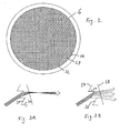
- the inventive lens device 6 is a single combination lens fabricated as one piece and consisting a plurality of single lenses 26, each having differing optical angular intensity distribution.
- the combination lens 6 includes and combines the optical features of a collecting lens as well as of a fresnel lens and of a multiple filter or screening device and a antireflection device in one single optical device.
- the combination lens 6 has a first surface area 27, which is facing the light source and comprises an internal structure, and a second surface area 28, which is curved, but has no structured surface, and is turned away with respect to the light source.
- the internal structure of said first surface area 27 of the combination lens 6 is formed by polygonal or round area parts arranged side by side, and is formed especially by 4- or (as shown in the Figures) 6-cornered area parts or (not shown) by circular or oval area parts.
- every single lens 26 has a curved or bent surface part 30 on the surface 26 facing the light source, said surface part 30 either having a concave form according to Figure 3A , or having a convex form according to Figure 3B , and having a linear surface part 31 joining therewith.
- Every single lens 26 has an individual form which is either determined empirically or by calculation, namely in such way that in accordance with the the form and/or the direction of the angle of every polygonal or round surface part 30, 31 with respect to the optical axis of the signal lamp the light radiated from the light source is individually directed into specific directions on the basis of user specified orders.
- the LED light is directed according to the predetermined angular intensity distribution due to the angle and position of every polygonal surface.
- the light radiation is formed such according to the defined curving or bending of the concave or convex surface parts 30 that the predetermined angular intensity distribution is fulfilled. Consequently, as less as possible light is wasted, therefore the efficiency is increased significantly.
- a good uniformity concerning the light density is achieved, as every honeycomb like single lens 26 generates individual the wished angular intensity distribution, wherein additionally also the mixing of colors is generated in each single lens.
- the signal light of the invention appears as a smooth regularly illuminated light area.
- the geometry of the internal structure of the lens could be designed such that less or even no light is directed to non-wished directions to the external, therefore still increasing the efficiency of the signal lamp.
- the lens device 6 in addition works with respect to a further reduction of phantom light.
- anti reflection areas 32 could be formed on the inside or outside of the lens device (by roughing, matting, coloring or printing), and in particular individual for each single lens. With such anti reflection areas 32, reflections stemming from the internal lens structure can be avoided by absorption or divergence.
- the form, size and position of such anti reflection areas 32 can vary dependent of the position and angle of each single lens within the lens device 6.
- TIR Total Internal Reflection
- a "total internal reflection” may be used within the material itself.
- Figures 6, 7 and 8 show details of such TIR-zones 36 at the edge regions of the lens device 6.
- a specific feature of the present invention is further that the number, the position and the distance of the light means 3 on the circuit board 10 can variable be settled dependent on the user specifications. Furthermore, the position of the circuit board 10 on the basis support 2 can be set with predetermined position limits, in order to optimize the angular intensity distribution of the signal lamp 1.
- the circuit board 10 has on its contacting surface several prefabricated pads 33 for contacting the light means or LEDs 3. In the disclosed embodiment (see Figure 4 ), a number of ten pads 33 are arranged in the form of a triangle. Some of them are used for the contact with the light means, wherein the number and arrangement of the contacted light means 3 depend on the user specified total light power, light performance and light characteristic to be fulfilled by the signal lamp.
- the circuit board 10 comprises several prefabricated boreholes 34 for securing the circuit board 10 on the basis support 2 through fastening means like screw connections or pins or other means, and said basis support 2 comprises several holes 35 for engaging said fastening means.
- the distance between said many holes 35 is rather narrow, in order to allow a geometric variable fixation of the circuit board 10 on the basis support within the plane of the basis support.
Landscapes
- Physics & Mathematics (AREA)
- General Physics & Mathematics (AREA)
- Non-Portable Lighting Devices Or Systems Thereof (AREA)
- Liquid Crystal (AREA)
- Optical Head (AREA)
- Optical Communication System (AREA)
- Traffic Control Systems (AREA)
- Led Device Packages (AREA)
Claims (18)
- Signalleuchte mit einem Grundträger (2) und elektrischen Leuchtmitteln (3), die eine quasi-zentrale Lichtquelle bilden und mit einem kleinen Abstand voneinander auf dem Grundträger (2) in einer Ebene (5) derart angeordnet sind, dass die von den Leuchtmitteln (3) eingenommene Fläche eine maximale Seitengröße aufweist, und mit einer Linseneinrichtung (6), die in einem vorbestimmten Abstand vor den Leuchtmitteln (3) derart angeordnet ist, dass der vorbestimmte Abstand wesentlich größer als die maximale Seitengröße ist, und wobei im Fall lediglich eines Leuchtmittels (3) die Position und im Fall von einigen Leuchtmitteln (3) die Position und die Abstände der Leuchtmittel gemäß anwenderspezifischen Variablen auf dem Grundträger (2) einstellbar sind.
- Signalleuchte nach Anspruch 1, gekennzeichnet durch eine die Leuchtmittel (3) halterende Leiterplatte (10), wobei die Leiterplatte auf ihrer Kontaktierungsoberfläche mehrere vorgefertigte Kontakt-Anschlussflächen zum Anschluss der Leuchtmittel (3) aufweist.
- Signalleuchte nach Anspruch 1 oder 2, dadurch gekennzeichnet, dass mehrere vorgefertigte Kontakt-Anschlussflächen in einer derartigen Weise angeordnet sind, dass eine beliebige Anzahl und Anordnung der Leuchtmitteln (3) in Abhängigkeit von dem vom Anwender festgelegten Gesamt-Lichtleistung, des Lichtverlaufs und der Leuchtcharakteristik durch die Signalleuchte erfüllt ist.
- Signalleuchte nach einem der vorhergehenden Ansprüche, dadurch gekennzeichnet, dass die Leiterplatte (10) mehrere vorgefertigte Bohrlöcher zur Befestigung der Leiterplatte (10) an dem Grundträger (2) über Befestigungsmittel, wie Schrauben oder Stiften oder andere Befestigungsmittel aufweist, und dass der Grundträger (2) mehrere Bohrlöcher zur Aufnahme der Befestigungsmittel aufweist.
- Signalleuchte nach einem der vorhergehenden Ansprüche, dadurch gekennzeichnet, dass ein Abstandshalter zwischen der Leiterplatte (10) und dem Grundträger (2) zur veränderbaren Positionierung der Leuchtmittel (3) bezüglich der Höhe der Leuchtmittel (3) vorgesehen ist.
- Signalleuchte nach einem der vorhergehenden Ansprüche, dadurch gekennzeichnet, dass der Grundträger (2) ein Kühlelement (12) auf der Rückseite des Grundträgers (2) aufweist, wobei die Rückseite auf der den Leuchtmitteln (3) gegenüberliegenden Seite liegt.
- Signalleuchte nach einem der vorhergehenden Ansprüche, dadurch gekennzeichnet, dass das eine oder die mehreren Leuchtmittel (3) und eine elektrische Verdrahtung (9), die einer Ansteuereinrichtung und einer Leistungsversorgung der Leuchtmitteln (3) entspricht, auf lediglich einer einzigen Leiterplatte (10) angeordnet sind, wobei die Leiterplatte (10) mit dem Kühlelement (12) über wärmeleitendes Material (11) gekoppelt ist.
- Signalleuchte nach einem der vorhergehenden Ansprüche, dadurch gekennzeichnet, dass das Kühlelement (12) durch einen passiven Kühlkörper oder ein Wärmespeicherelement gebildet ist.
- Signallampe mit einem Grundträger (2) und elektrischen Leuchtmitteln (3), die eine quasi-zentrale Lichtquelle darstellen und mit einem geringen Abstand zwischen einander auf dem Grundträger (2) in einer Ebene (5) derart angeordnet sind, dass die von den Leuchtmitteln (3) eingenommene Fläche eine maximale Seitengröße aufweist, und mit einer Linseneinrichtung (6), die in einem vorbestimmten Abstand vor den Leuchtmitteln derart angeordnet ist, dass der vorbestimmte Abstand wesentlich größer als die maximale Seitengröße ist, und wobei die Linseneinrichtung (6) lediglich eine einzige Kombinationslinse umfasst, die aus einer Vielzahl von Einzellinsen besteht, die jeweils eine unterschiedliche optische Winkel-Intensitätsverteilung aufweisen.
- Signalleuchte nach einem der vorhergehenden Ansprüche, dadurch gekennzeichnet, dass die Kombinationslinse (6) eine erste Oberfläche (27), die auf die Lichtquelle gerichtet ist und eine Innenstruktur aufweist, und eine zweite Oberfläche (28) aufweist, die gewölbt und von der Lichtquelle abgewandt ist.
- Signalleuchte nach einem der vorhergehenden Ansprüche, dadurch gekennzeichnet, dass die Innenstruktur der ersten Oberfläche (27) der Kombinationslinse (6) durch vieleckige oder runde Flächenabschnitte gebildet ist und insbesondere durch vier- oder sechseckige Flächenabschnitte oder kreisförmige oder ovale Flächenabschnitte gebildet ist.
- Signalleuchte nach einem der vorhergehenden Ansprüche, dadurch gekennzeichnet, dass das von der Lichtquelle abgestrahlte Licht in vorbestimmten Richtungen verteilt wird, die entsprechend anwenderspezifischen Vorgaben durch Einstellen des Winkels jedes vieleckigen oder runden Flächenabschnittes gegenüber der optischen Achse der Signalleuchte einstellbar sind.
- Signalleuchte nach einem der vorhergehenden Ansprüche, dadurch gekennzeichnet, dass die Kombinationslinse (6) Antireflex-Flächen (32) aufweist, die in unterschiedlicher Weise auf der Innenseite oder Außenseite der Oberfläche hinsichtlich der Form, der Größe und der Position der Antireflex-Flächen ausgebildet sind.
- Signalleuchte nach einem der vorhergehenden Ansprüche, dadurch gekennzeichnet, dass die Antireflex-Flächen durch Aufrauen, Mattieren, Einfärben oder Bedrucken der Linsenoberfläche ausgebildet sind.
- Signalleuchte mit einem Grundträger (2) und elektrischen Leuchtmitteln (3), die eine quasi-zentrale Lichtquelle darstellen und mit einem geringen Abstand voneinander auf dem Grundträger (2) in einer Ebene (5) derart angeordnet sind, dass die von den Leuchtmitteln (3) eingenommene Fläche eine maximale Seitengröße aufweist, und mit einer Linseneinrichtung (6), die in einem vorbestimmten Abstand vor den Leuchtmitteln (3) derart angeordnet ist, dass der vorbestimmte Abstand wesentlich größer als die maximale Seitengröße ist, und wobei das zumindest eine Leuchtmittel (3) auf einer einzigen Leiterplatte (10) angeordnet ist, wobei die Leiterplatte auch die elektrischen Schaltungen zur Ansteuerung und Leistungsversorgung der Leuchtmittel aufnimmt und ein aus einem lichtabsorbierenden Material, vorzugsweise aus Kunststoff, hergestelltes Formteil (14) die Leiterplatte (10) vollständig überdeckt.
- Signalleuchte nach Anspruch (15), dadurch gekennzeichnet, dass das Formteil (14) einen sich nach außen erstreckenden Flügelteil (15), einen Mittelteil (16) und einen geneigten Wandteil (17) umfasst, der den Flügelteil (15) und den Mittelteil (16) verbindet, wobei die Teile (15, 16, 17) des Formteils (14) alle reflektierenden Teile auf dem Grundträger (2) oder der Leiterplatte (10) gegenüber unerwünschten Lichtreflexionen abschirmen.
- Signalleuchte nach Anspruch 16, dadurch gekennzeichnet, dass das Formteil (14) Bohrlöcher oder Öffnungen (18) aufweist, in die die Leuchtmittel (13) eingesetzt sind.
- Signalleuchte nach einem der vorhergehenden Ansprüche, dadurch gekennzeichnet, dass die Leuchtmittel (3) Lumineszenzdioden, insbesondere Hochleistungs-Lumineszenzdioden sind.
Applications Claiming Priority (2)
| Application Number | Priority Date | Filing Date | Title |
|---|---|---|---|
| DE10354176A DE10354176A1 (de) | 2003-11-19 | 2003-11-19 | Signalleuchte |
| DE10354176 | 2003-11-19 |
Publications (2)
| Publication Number | Publication Date |
|---|---|
| EP1533774A1 EP1533774A1 (de) | 2005-05-25 |
| EP1533774B1 true EP1533774B1 (de) | 2009-03-25 |
Family
ID=34428815
Family Applications (1)
| Application Number | Title | Priority Date | Filing Date |
|---|---|---|---|
| EP04013321A Expired - Lifetime EP1533774B1 (de) | 2003-11-19 | 2004-06-05 | Signalleuchte |
Country Status (4)
| Country | Link |
|---|---|
| EP (1) | EP1533774B1 (de) |
| AT (1) | ATE426877T1 (de) |
| DE (2) | DE10354176A1 (de) |
| WO (1) | WO2005050588A1 (de) |
Cited By (1)
| Publication number | Priority date | Publication date | Assignee | Title |
|---|---|---|---|---|
| RU2619678C2 (ru) * | 2013-03-27 | 2017-05-17 | Сименс Акциенгезелльшафт | Светофор |
Families Citing this family (6)
| Publication number | Priority date | Publication date | Assignee | Title |
|---|---|---|---|---|
| DE602006010949D1 (de) | 2005-10-07 | 2010-01-21 | Black & Decker Inc | Tragbare Leuchte |
| RU2308060C1 (ru) * | 2006-04-12 | 2007-10-10 | Закрытое акционерное общество "Светлана-Оптоэлектроника" | Светорассеивающая линза для светофора |
| EP1925874B8 (de) | 2006-11-24 | 2014-09-10 | OSRAM GmbH | LED Farbmischung Beleuchtungssystem |
| DE102007047461A1 (de) | 2007-09-28 | 2009-04-02 | Carl Zeiss Microimaging Gmbh | Verfahren und optische Anordnung zur Untersuchung einer Probe |
| DE102014204968A1 (de) * | 2014-03-18 | 2015-09-24 | Siemens Aktiengesellschaft | Signalgeber zur Abgabe eines Lichtsignals |
| EP3007147A1 (de) * | 2014-10-06 | 2016-04-13 | Dialight Garufo GmbH | Verkehrssignalgeber |
Family Cites Families (7)
| Publication number | Priority date | Publication date | Assignee | Title |
|---|---|---|---|---|
| ES2135619T3 (es) * | 1994-07-22 | 1999-11-01 | Siemens Schweiz Ag | Luz de señalizacion. |
| DE10010606A1 (de) * | 2000-03-03 | 2001-09-06 | Wts Kereskedelmi Es Szolgaltat | Beleuchtungskörper für Feuchträume aller Art |
| US20020085390A1 (en) * | 2000-07-14 | 2002-07-04 | Hironobu Kiyomoto | Optical device and apparatus employing the same |
| US6323781B1 (en) * | 2000-08-22 | 2001-11-27 | Power Signal Technologies | Electronically steerable light output viewing angles for traffic signals |
| JP2002260597A (ja) * | 2001-02-28 | 2002-09-13 | Harison Toshiba Lighting Corp | 光源装置及び実装回路装置 |
| US6585395B2 (en) * | 2001-03-22 | 2003-07-01 | Altman Stage Lighting Co., Inc. | Variable beam light emitting diode light source system |
| US6955449B2 (en) * | 2001-04-13 | 2005-10-18 | Gelcore Llc | LED symbol signal |
-
2003
- 2003-11-19 DE DE10354176A patent/DE10354176A1/de not_active Withdrawn
-
2004
- 2004-06-05 EP EP04013321A patent/EP1533774B1/de not_active Expired - Lifetime
- 2004-06-05 AT AT04013321T patent/ATE426877T1/de not_active IP Right Cessation
- 2004-06-05 DE DE602004020168T patent/DE602004020168D1/de not_active Expired - Lifetime
- 2004-11-16 WO PCT/EP2004/012987 patent/WO2005050588A1/en not_active Ceased
Cited By (1)
| Publication number | Priority date | Publication date | Assignee | Title |
|---|---|---|---|---|
| RU2619678C2 (ru) * | 2013-03-27 | 2017-05-17 | Сименс Акциенгезелльшафт | Светофор |
Also Published As
| Publication number | Publication date |
|---|---|
| DE10354176A1 (de) | 2005-08-04 |
| DE602004020168D1 (de) | 2009-05-07 |
| WO2005050588A1 (en) | 2005-06-02 |
| ATE426877T1 (de) | 2009-04-15 |
| EP1533774A1 (de) | 2005-05-25 |
Similar Documents
| Publication | Publication Date | Title |
|---|---|---|
| US7407307B2 (en) | Illuminating panel and illuminating device | |
| US7794128B2 (en) | Lamp unit of vehicle headlamp | |
| RU2459142C1 (ru) | Уличный фонарь на светодиодах | |
| US7686475B2 (en) | Lighting fixture | |
| EP1697685B1 (de) | Leuchtdioden (leds) mit hoher strahlungsleistung verwendende reflektoranordnungen | |
| EP1916468B1 (de) | LED-Beleuchtungshalterung | |
| US6637921B2 (en) | Replaceable LED bulb with interchangeable lens optic | |
| US7794126B2 (en) | Vehicle lamp | |
| US20080298062A1 (en) | Led illumination device | |
| KR101497482B1 (ko) | 조명 모듈 | |
| US6616299B2 (en) | Single optical element LED signal | |
| JP5147357B2 (ja) | 道路照明装置 | |
| US7300185B1 (en) | Quadrilateral symmetrical light source | |
| KR20120027222A (ko) | 조명 장치용 반사기 시스템 | |
| CN101725853A (zh) | 发光二极管模块、以及利用发光二极管模块的灯具和照明方法 | |
| EP2385294B1 (de) | Beleuchtungsvorrichtung mit austauschbaren Modulen | |
| JP2005150036A (ja) | Led照明装置及び車両用灯具 | |
| KR101197716B1 (ko) | 도로조명용 가로등 유닛 | |
| JP2004193031A (ja) | Led照明装置 | |
| EP2321575B1 (de) | Led-reflektor und leuchte damit | |
| JPS61214000A (ja) | 全方向性の信号灯 | |
| EP1533774A1 (de) | Signalleuchte | |
| KR102621888B1 (ko) | 차량용 조명 장치 | |
| KR102621885B1 (ko) | 차량용 조명 장치 | |
| JPH038204A (ja) | Ledランプ装置 |
Legal Events
| Date | Code | Title | Description |
|---|---|---|---|
| PUAI | Public reference made under article 153(3) epc to a published international application that has entered the european phase |
Free format text: ORIGINAL CODE: 0009012 |
|
| AK | Designated contracting states |
Kind code of ref document: A1 Designated state(s): AT BE BG CH CY CZ DE DK EE ES FI FR GB GR HU IE IT LI LU MC NL PL PT RO SE SI SK TR |
|
| AX | Request for extension of the european patent |
Extension state: AL HR LT LV MK |
|
| 17P | Request for examination filed |
Effective date: 20051125 |
|
| AKX | Designation fees paid |
Designated state(s): AT BE BG CH CY CZ DE DK EE ES FI FR GB GR HU IE IT LI LU MC NL PL PT RO SE SI SK TR |
|
| AXX | Extension fees paid |
Extension state: MK Payment date: 20051125 Extension state: LV Payment date: 20051125 Extension state: AL Payment date: 20051125 Extension state: LT Payment date: 20051125 |
|
| RIN1 | Information on inventor provided before grant (corrected) |
Inventor name: LOMBERG, MARKUS Inventor name: HERTRICH, MICHAEL |
|
| GRAP | Despatch of communication of intention to grant a patent |
Free format text: ORIGINAL CODE: EPIDOSNIGR1 |
|
| GRAS | Grant fee paid |
Free format text: ORIGINAL CODE: EPIDOSNIGR3 |
|
| GRAA | (expected) grant |
Free format text: ORIGINAL CODE: 0009210 |
|
| AK | Designated contracting states |
Kind code of ref document: B1 Designated state(s): AT BE BG CH CY CZ DE DK EE ES FI FR GB GR HU IE IT LI LU MC NL PL PT RO SE SI SK TR |
|
| AX | Request for extension of the european patent |
Extension state: AL LT LV MK |
|
| REG | Reference to a national code |
Ref country code: GB Ref legal event code: FG4D |
|
| REG | Reference to a national code |
Ref country code: CH Ref legal event code: EP |
|
| REG | Reference to a national code |
Ref country code: IE Ref legal event code: FG4D |
|
| REF | Corresponds to: |
Ref document number: 602004020168 Country of ref document: DE Date of ref document: 20090507 Kind code of ref document: P |
|
| PG25 | Lapsed in a contracting state [announced via postgrant information from national office to epo] |
Ref country code: FI Free format text: LAPSE BECAUSE OF FAILURE TO SUBMIT A TRANSLATION OF THE DESCRIPTION OR TO PAY THE FEE WITHIN THE PRESCRIBED TIME-LIMIT Effective date: 20090325 Ref country code: SI Free format text: LAPSE BECAUSE OF FAILURE TO SUBMIT A TRANSLATION OF THE DESCRIPTION OR TO PAY THE FEE WITHIN THE PRESCRIBED TIME-LIMIT Effective date: 20090325 |
|
| LTIE | Lt: invalidation of european patent or patent extension |
Effective date: 20090325 |
|
| PG25 | Lapsed in a contracting state [announced via postgrant information from national office to epo] |
Ref country code: AT Free format text: LAPSE BECAUSE OF FAILURE TO SUBMIT A TRANSLATION OF THE DESCRIPTION OR TO PAY THE FEE WITHIN THE PRESCRIBED TIME-LIMIT Effective date: 20090325 Ref country code: SE Free format text: LAPSE BECAUSE OF FAILURE TO SUBMIT A TRANSLATION OF THE DESCRIPTION OR TO PAY THE FEE WITHIN THE PRESCRIBED TIME-LIMIT Effective date: 20090625 Ref country code: PL Free format text: LAPSE BECAUSE OF FAILURE TO SUBMIT A TRANSLATION OF THE DESCRIPTION OR TO PAY THE FEE WITHIN THE PRESCRIBED TIME-LIMIT Effective date: 20090325 |
|
| NLV1 | Nl: lapsed or annulled due to failure to fulfill the requirements of art. 29p and 29m of the patents act | ||
| PG25 | Lapsed in a contracting state [announced via postgrant information from national office to epo] |
Ref country code: BE Free format text: LAPSE BECAUSE OF FAILURE TO SUBMIT A TRANSLATION OF THE DESCRIPTION OR TO PAY THE FEE WITHIN THE PRESCRIBED TIME-LIMIT Effective date: 20090325 |
|
| PG25 | Lapsed in a contracting state [announced via postgrant information from national office to epo] |
Ref country code: CZ Free format text: LAPSE BECAUSE OF FAILURE TO SUBMIT A TRANSLATION OF THE DESCRIPTION OR TO PAY THE FEE WITHIN THE PRESCRIBED TIME-LIMIT Effective date: 20090325 Ref country code: EE Free format text: LAPSE BECAUSE OF FAILURE TO SUBMIT A TRANSLATION OF THE DESCRIPTION OR TO PAY THE FEE WITHIN THE PRESCRIBED TIME-LIMIT Effective date: 20090325 Ref country code: PT Free format text: LAPSE BECAUSE OF FAILURE TO SUBMIT A TRANSLATION OF THE DESCRIPTION OR TO PAY THE FEE WITHIN THE PRESCRIBED TIME-LIMIT Effective date: 20090901 Ref country code: ES Free format text: LAPSE BECAUSE OF FAILURE TO SUBMIT A TRANSLATION OF THE DESCRIPTION OR TO PAY THE FEE WITHIN THE PRESCRIBED TIME-LIMIT Effective date: 20090706 |
|
| PG25 | Lapsed in a contracting state [announced via postgrant information from national office to epo] |
Ref country code: SK Free format text: LAPSE BECAUSE OF FAILURE TO SUBMIT A TRANSLATION OF THE DESCRIPTION OR TO PAY THE FEE WITHIN THE PRESCRIBED TIME-LIMIT Effective date: 20090325 Ref country code: NL Free format text: LAPSE BECAUSE OF FAILURE TO SUBMIT A TRANSLATION OF THE DESCRIPTION OR TO PAY THE FEE WITHIN THE PRESCRIBED TIME-LIMIT Effective date: 20090325 Ref country code: RO Free format text: LAPSE BECAUSE OF FAILURE TO SUBMIT A TRANSLATION OF THE DESCRIPTION OR TO PAY THE FEE WITHIN THE PRESCRIBED TIME-LIMIT Effective date: 20090325 |
|
| PG25 | Lapsed in a contracting state [announced via postgrant information from national office to epo] |
Ref country code: BG Free format text: LAPSE BECAUSE OF FAILURE TO SUBMIT A TRANSLATION OF THE DESCRIPTION OR TO PAY THE FEE WITHIN THE PRESCRIBED TIME-LIMIT Effective date: 20090625 Ref country code: DK Free format text: LAPSE BECAUSE OF FAILURE TO SUBMIT A TRANSLATION OF THE DESCRIPTION OR TO PAY THE FEE WITHIN THE PRESCRIBED TIME-LIMIT Effective date: 20090325 Ref country code: MC Free format text: LAPSE BECAUSE OF NON-PAYMENT OF DUE FEES Effective date: 20090630 |
|
| PLBE | No opposition filed within time limit |
Free format text: ORIGINAL CODE: 0009261 |
|
| REG | Reference to a national code |
Ref country code: CH Ref legal event code: PL |
|
| STAA | Information on the status of an ep patent application or granted ep patent |
Free format text: STATUS: NO OPPOSITION FILED WITHIN TIME LIMIT |
|
| GBPC | Gb: european patent ceased through non-payment of renewal fee |
Effective date: 20090625 |
|
| 26N | No opposition filed |
Effective date: 20091229 |
|
| REG | Reference to a national code |
Ref country code: FR Ref legal event code: ST Effective date: 20100226 |
|
| PG25 | Lapsed in a contracting state [announced via postgrant information from national office to epo] |
Ref country code: LI Free format text: LAPSE BECAUSE OF NON-PAYMENT OF DUE FEES Effective date: 20090630 Ref country code: IE Free format text: LAPSE BECAUSE OF NON-PAYMENT OF DUE FEES Effective date: 20090605 Ref country code: FR Free format text: LAPSE BECAUSE OF NON-PAYMENT OF DUE FEES Effective date: 20090630 Ref country code: CH Free format text: LAPSE BECAUSE OF NON-PAYMENT OF DUE FEES Effective date: 20090630 |
|
| PG25 | Lapsed in a contracting state [announced via postgrant information from national office to epo] |
Ref country code: GB Free format text: LAPSE BECAUSE OF NON-PAYMENT OF DUE FEES Effective date: 20090625 |
|
| PG25 | Lapsed in a contracting state [announced via postgrant information from national office to epo] |
Ref country code: GR Free format text: LAPSE BECAUSE OF FAILURE TO SUBMIT A TRANSLATION OF THE DESCRIPTION OR TO PAY THE FEE WITHIN THE PRESCRIBED TIME-LIMIT Effective date: 20090626 |
|
| PG25 | Lapsed in a contracting state [announced via postgrant information from national office to epo] |
Ref country code: IT Free format text: LAPSE BECAUSE OF FAILURE TO SUBMIT A TRANSLATION OF THE DESCRIPTION OR TO PAY THE FEE WITHIN THE PRESCRIBED TIME-LIMIT Effective date: 20090325 |
|
| PG25 | Lapsed in a contracting state [announced via postgrant information from national office to epo] |
Ref country code: LU Free format text: LAPSE BECAUSE OF NON-PAYMENT OF DUE FEES Effective date: 20090605 |
|
| PG25 | Lapsed in a contracting state [announced via postgrant information from national office to epo] |
Ref country code: HU Free format text: LAPSE BECAUSE OF FAILURE TO SUBMIT A TRANSLATION OF THE DESCRIPTION OR TO PAY THE FEE WITHIN THE PRESCRIBED TIME-LIMIT Effective date: 20090926 |
|
| PG25 | Lapsed in a contracting state [announced via postgrant information from national office to epo] |
Ref country code: TR Free format text: LAPSE BECAUSE OF FAILURE TO SUBMIT A TRANSLATION OF THE DESCRIPTION OR TO PAY THE FEE WITHIN THE PRESCRIBED TIME-LIMIT Effective date: 20090325 |
|
| PG25 | Lapsed in a contracting state [announced via postgrant information from national office to epo] |
Ref country code: CY Free format text: LAPSE BECAUSE OF FAILURE TO SUBMIT A TRANSLATION OF THE DESCRIPTION OR TO PAY THE FEE WITHIN THE PRESCRIBED TIME-LIMIT Effective date: 20090325 |
|
| REG | Reference to a national code |
Ref country code: DE Ref legal event code: R119 Ref document number: 602004020168 Country of ref document: DE Effective date: 20140101 |
|
| PG25 | Lapsed in a contracting state [announced via postgrant information from national office to epo] |
Ref country code: DE Free format text: LAPSE BECAUSE OF NON-PAYMENT OF DUE FEES Effective date: 20140101 |
|
| REG | Reference to a national code |
Ref country code: DE Ref legal event code: R073 Ref document number: 602004020168 Country of ref document: DE |
|
| REG | Reference to a national code |
Ref country code: DE Ref legal event code: R074 Ref document number: 602004020168 Country of ref document: DE |
|
| PGRI | Patent reinstated in contracting state [announced from national office to epo] |
Ref country code: DE Effective date: 20150921 |
|
| PGFP | Annual fee paid to national office [announced via postgrant information from national office to epo] |
Ref country code: DE Payment date: 20151223 Year of fee payment: 12 |
|
| REG | Reference to a national code |
Ref country code: DE Ref legal event code: R119 Ref document number: 602004020168 Country of ref document: DE |
|
| PG25 | Lapsed in a contracting state [announced via postgrant information from national office to epo] |
Ref country code: DE Free format text: LAPSE BECAUSE OF NON-PAYMENT OF DUE FEES Effective date: 20170103 |