EP1533723A2 - Verfahren, Gerät und computerlesbares Medium zur Simulation und zur Visualisierung der Datenübertragung zwischen einem Emulationssystem und einem Simulator - Google Patents
Verfahren, Gerät und computerlesbares Medium zur Simulation und zur Visualisierung der Datenübertragung zwischen einem Emulationssystem und einem Simulator Download PDFInfo
- Publication number
- EP1533723A2 EP1533723A2 EP04027295A EP04027295A EP1533723A2 EP 1533723 A2 EP1533723 A2 EP 1533723A2 EP 04027295 A EP04027295 A EP 04027295A EP 04027295 A EP04027295 A EP 04027295A EP 1533723 A2 EP1533723 A2 EP 1533723A2
- Authority
- EP
- European Patent Office
- Prior art keywords
- controller
- simulator
- interface
- data
- cable
- Prior art date
- Legal status (The legal status is an assumption and is not a legal conclusion. Google has not performed a legal analysis and makes no representation as to the accuracy of the status listed.)
- Withdrawn
Links
Images




Classifications
-
- G—PHYSICS
- G06—COMPUTING OR CALCULATING; COUNTING
- G06F—ELECTRIC DIGITAL DATA PROCESSING
- G06F30/00—Computer-aided design [CAD]
- G06F30/30—Circuit design
- G06F30/32—Circuit design at the digital level
- G06F30/33—Design verification, e.g. functional simulation or model checking
- G06F30/3308—Design verification, e.g. functional simulation or model checking using simulation
- G06F30/331—Design verification, e.g. functional simulation or model checking using simulation with hardware acceleration, e.g. by using field programmable gate array [FPGA] or emulation
-
- G—PHYSICS
- G06—COMPUTING OR CALCULATING; COUNTING
- G06F—ELECTRIC DIGITAL DATA PROCESSING
- G06F30/00—Computer-aided design [CAD]
- G06F30/30—Circuit design
- G06F30/32—Circuit design at the digital level
- G06F30/33—Design verification, e.g. functional simulation or model checking
-
- G—PHYSICS
- G06—COMPUTING OR CALCULATING; COUNTING
- G06F—ELECTRIC DIGITAL DATA PROCESSING
- G06F2117/00—Details relating to the type or aim of the circuit design
- G06F2117/08—HW-SW co-design, e.g. HW-SW partitioning
Definitions
- the field of the invention relates generally to hardware and software verification of logic circuits and more particularly relates to a communication protocol and communication control hardware that optimizes the bandwidth and latency of data transfer between a program running on a workstation and a hardware verification system.
- DUV design under verification
- the DUV is usually provided in the form of a netlist description of the design.
- the netlist may have been derived from many sources, including from a hardware description language.
- a netlist description (or "netlist”, as it is referred to by those of ordinary skill in the art) is a description of the circuit's components and electrical interconnections between the components.
- the components include all those circuit elements necessary for implementing a logic circuit, such as combinational logic (e.g., gates) and sequential logic (e.g., flip-flops and latches).
- Design verification is performed because fabricating an integrated circuit is expensive and takes time. If the circuit design contains functional errors, the design will have to be corrected and then re-fabricated. Thus, many different platforms for functional verification of integrated circuits have been developed. Hardware-based design verification systems such as logic emulation systems are known devices that implement a user's design in a plurality of programmable integrated circuits. Such logic emulation systems are available from various vendors, including Cadence Design Systems, Inc., San Jose, California, United States of America, and others.
- Typical emulation systems utilize either programmable logic chips or processor chips that are programmably interconnected.
- processor-based emulation systems the DUV is processed so that its functionality appears to be created in the processors by calculating the outputs of the design.
- the logic itself is not implemented in a processor-based emulation system. Examples of hardware logic emulation systems using processor chips can be seen in, e.g., United States Patent Nos. 5,551,013, 6,035,117 and 6,051,030.
- a testbench is a series of test vectors (i.e., stimulus) that are used to stimulate a design and may include modules that receive the outputs from the DUV after the vectors are run in the DUV. Since most electronic designs are presently designed using hardware description languages (“HDL”) such as Verilog, a testbench is typically comprised of some HDL code.
- HDL hardware description languages
- Hardware-based verification systems and software-based verification systems each have benefits that the other lacks.
- software-based verification systems allow for very accurate verification using the exact timing (i.e., clocking) that the actual DUV will encounter when installed in a real electronic system.
- Software simulators allow a user to see the result of every logic operation and can graphically represent the signal transitions from high to low or from low to high on a computer monitor. While hardware-based verifications systems do not normally have this ability, hardware-based systems are orders of magnitude faster than software-based systems and therefore provide very fast verification.
- a third approach is to emulate the DUV using an emulator that allows full visibility for a fixed size of trace window.
- the emulator is running freely, and signals generated by the DUV in the emulator that allow for full vision are saved for a certain period of time.
- a final approach is to emulate the DUV with an emulator that provides for limited visibility and replay. With this approach, limited information is saved during emulation. Designers might need to run emulation a few times in order to get sufficient information for analysis.
- one way of using a hardware-based verification system is in conjunction with a software simulator. This is sometimes referred to as simulation acceleration. Because emulators operate at speeds that can be orders of magnitude faster than simulators, emulation systems, and in particular, processor-based emulation systems, contain vast amounts of information about the state and activity in the emulated circuit. The reason for this is as follows. Simulators allow designers to view the state of a signal as it exists at a specific node in the DUV at a specific time (i.e., clock cycle) immediately after a single cycle of a simulation. A simulation cycle is the amount of time (and thus the state changes that take place) during one step of the fastest clock driving the DUV. In other words, a simulation cycle is the time of interest during a verification operation because any signal transitions that take place during simulation cycle are typically not relevant. The only signal transitions that generally are important in a DUV are the signal transitions that exist at the end of one simulation cycle.
- the stimuli that drive the DUV during a simulation cycle are modeled on the workstation.
- the stimuli driving the DUV are sent to the emulator that is emulating the DUV, and the response is then sent back to the simulator. Because emulators run the DUVs at clock speeds that are dramatically faster than simulators, simulation acceleration can dramatically decrease the amount of time it takes to verify a DUV.
- Simulation engines need constant access to this state information in order to make simulation acceleration worthwhile.
- Simulation engines also need immediate responses to state changes in the emulated circuit to continue simulation, which requires low latency (i.e. the simulator and the emulator generally need to run in lockstep mode).
- the sheer volume of data required and made available in a large emulation requires a high bandwidth connection.
- the cycle time for simulation acceleration is generally defined as the amount of time it takes to send signals from the simulator to the emulator, the time the emulator takes to calculate what changes occurred in the signals running through the DUV, and the time required to send those changes back to the simulator running in the workstation. Latency, which is a key issue in simulation acceleration, is the amount of time it takes to get a response from the emulator. For simulation acceleration to be a useful verification method, latency must be reduced as much as possible.
- the software simulator accesses the states of the emulator by querying the emulator through a high latency Ethernet path to a local processor in the emulator and then across an address/data handshake path to access individual components in the emulation system.
- the Direct Attach Stimulus (“DAS") interface connects to a series of register circuits programmed into the emulated logic of the DUV. Software simulation accesses are grouped into a burst of data into and/or out of these registers.
- This burst of data is transferred across a 31 bit data path between the emulated registers and a memory buffer on the PCI card in the workstation.
- the simulator hands the data to a "DAS driver", which formats it and transfers it to the PCI memory buffer and initiates the transfer. Once complete, the driver transfers the return data back to the simulator's buffer.
- the DAS card is a product available from Cadence Design Systems, Inc., San Jose, California, that provides for communication between a simulator running in a workstation or personal computer and an emulator.
- a problem with the first prior approach is that the network path to the embedded processor in the emulation system has very high latency due to the reaction time of the local processor that receives the request, accesses the appropriate element(s) in the emulation engine, then formulates a response, and sends it across the network to the workstation application.
- a method of transferring data between a simulator and an emulator across an interface comprises updating a simulator buffer of the simulator to contain a desired input state for an emulation cycle.
- a target write to the interface is performed to indicate that the emulation cycle can proceed.
- the emulation cycle is completed using an instruction sequencer within the interface independent of the simulator.
- Figure 1 illustrates a block diagram of an exemplary high-speed interface, according to one embodiment of the present invention
- Figure 2 illustrates a block diagram showing exemplary data paths of the interface 20, according to one embodiment of the present invention
- Figure 3 illustrates exemplary logic control paths for an interface 20, according to one embodiment of the present invention
- Figure 4 illustrates a diagram of an exemplary RAM pipeline datapath, according to one embodiment of the present invention
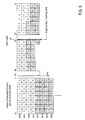
- Figure 5 illustrates a diagram of exemplary wide cable mode bit mapping, according to one embodiment of the present invention.
- Figure 6 illustrates an exemplary flow diagram of an exemplary transfer of data from the simulator to the emulator, according to one embodiment of the present invention.
- a method of transferring data between a simulator running in a workstation and an emulator across an interface comprises updating a simulator buffer of the simulator to contain a desired input state for an emulation cycle.
- a target write to the interface is performed to indicate that the emulation cycle can proceed.
- the emulation cycle is completed using an instruction sequencer within the interface independent of the simulator.
- the present invention also relates to apparatus for performing the operations herein.
- This apparatus may be specially constructed for the required purposes, or it may comprise a general-purpose computer selectively activated or reconfigured by a computer program stored in the computer.
- a computer program may be stored in a computer readable storage medium, such as, but is not limited to, any type of disk including floppy disks, optical disks, CD-ROMs, and magnetic-optical disks, read-only memories (ROMs), random access memories (RAMs), EPROMs, EEPROMs, magnetic or optical cards, or any type of media suitable for storing electronic instructions, and each coupled to a computer system bus.
- the various embodiments disclosed herein minimize effects of delays in transferring data between workstation and emulator by providing DMA control and optimizing the PCI transfers. These embodiments also minimize the setup required to initiate and complete a data transfer. A wider datapath also increases bandwidth.
- the various embodiments employ an architecture that includes a packetized transfer protocol that injects stimulus and extracts data directly from the emulation logic (hence the name: direct attach stimulus) by interfacing with control logic embedded in the emulated circuit, which organizes the data of interest into packets, and controls the transfer to synchronize it to the emulation circuitry.
- FIG. 1 illustrates a block diagram of an exemplary high-speed interface, according to one embodiment.
- interface 20 is a low latency interface between a workstation 10 running simulation programs and an emulation system 30.
- a workstation 10 has a central processing unit (“CPU") 15 that can execute computer instructions, including instructions forming a software simulation program.
- the workstation can be any type of computing device including a personal computer, etc.
- Workstation 10 also has memory in the form of random access memory (RAM) 18 that is in communication with the CPU 15.
- RAM random access memory
- CPU 15 is also connected to the interface 20.
- Interface 20 is in communication with a hardware-based functional verification device 30 such as an emulation system though a cable 35.
- Interface 20 comprises an I/O processor 22 that communicates with direct memory access (“DMA") module 24.
- DMA 24 allows signals acquired from the emulation system 30 during hardware acceleration to be directly stored into the RAM 18 without the need to use the CPU 15.
- DMA direct memory access
- the interface 20 can be placed on a single card that can be inserted into the workstation 10.
- interface 20 communicates with the workstation through a Peripheral Component Interconnect bus 40, commonly referred to as a "PCI bus".
- PCI bus 40 is a standard bus that allows peripherals to communicate with a computer system such as a workstation.
- the workstation 10 may be a SUN Ultra 60, Ultra 80, Ultra 450, Blade 1000, HPJ6000, IBM RS/6000 F80, Dell Workstation 530, IBM Intellistation ZPro 6866, or similar computing device.
- the interface 20 allows signals to be transferred back and forth between the emulator 30 and the simulator running on the workstation 10 through the PCI bus 40 in the workstation 10.
- the interface 20 is necessary because the emulator can produce and receive far more signals than a PCI bus 40 can handle.
- the interface 20 gathers data directly from the RAM 18 and transfers it over interface 35 to the emulator 30 and simultaneously transfers data from the emulator 30 back into the RAM 18, utilizing the DMA 24.
- the PCI bus 40 lacks both the bandwidth and has far too much latency to allow design signals generated in the emulator to be evaluated in the simulator in a useful manner.
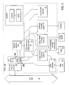
- FIG. 2 illustrates a block diagram showing exemplary data paths of the interface 20, according to one embodiment of the present invention.
- Interface 20 includes a PCI core 65 that acts as the interface between the PCI bus 40 and the remaining components of the interface 20.
- PCI core 65 implements standard PCI protocols so that interface 20 can place data on and receive data from the PCI bus 40.
- PCI core 65 can be implemented as a standard component that can be acquired from several different vendors. According to one embodiment, the PCI core 65 is provided by a Xilinx Virtex-II 64 bit, 66 MHz, Master/target IP core.
- a PCI controller 70 communicates with the PCI core 65.
- the PCI controller acts as the interface between the PCI core 65 and the rest of the interface 20. In presently preferred embodiments, there is no communication between the PCI core 65 and any other portion of the interface 20.
- PCI controller 70 allows access from the PCI bus 40 to memories and registers within the interface 20. In presently preferred embodiments, all accesses to and from the PCI bus 40 can be either thirty-two or sixty-four bits wide.
- the PCI controller 70 can act as PCI initiator of both read and write burst transfers to host memory.
- Interface 20 also comprises instruction sequencer ("IS") 50 that enables the interface 20 to perform sequences of operations.
- instruction sequences are as follows: Description Sequence of Opcodes Description Full emulation cycle PDN Download block to buffer CDN Download buffer to emulator CUP Upload from emulator, compare PUP Upload block to workstation memory PCIW Write done flag to workstation memory IDLE Idle. Full emulation cycle with status updates and streaming upload. PDN Download block to buffer PCIW Write status flag to workstation memory CDN Download buffer to emulator CUP Upload (partial data) from emulator, compare PCIW Write status flag to workstation memory.
- the exact sequence of instructions executed by the instruction sequencer 50 is at the discretion of programmer. This flexibility gives software a greater ability to optimize the operation of the system. This architecture also makes it easier for hardware to integrate new capabilities of enhancement, through expansion of the instruction set and by plugging into the appropriate parts of the logic design.
- the instruction sequencer 50 In the simplest mode, it would be possible for the instruction sequencer 50 to execute a very short sequence consisting of a single operation followed by a PCIW (PCI write word) to indicate completion. This would be useful to support the current API mode where individual operations are performed through single API calls.
- PCIW PCI write word
- Instruction sequencer 50 also initiates data transfers from or to a cable 35 that is in communication between the interface 20 and the emulator (not shown in Figure 2 ). According to one embodiment, the bandwidth of cable 35 is 96 MB/sec in each direction by having a 64-bit data path at 12MHz. A Molex LFH 200-pin connector can be used to connect the cable to the interface 20, according to one embodiment. Finally, instruction sequencer 50 initiates memory copy instructions, which perform DMA transfers to copy memory data between the interface RAM 75 across the PCI bus 40 into the workstation RAM (e.g., RAM 18 in Figure 1 ).
- the workstation RAM e.g., RAM 18 in Figure 1 .
- the instruction sequencer 50 receives instructions from an internal RAM 55 that stores instructions that are sequenced through the instruction sequencer 50.
- RAM 55 is internal FPGA RAM having 2MB of storage space.
- Exemplary instructions that are stored in the RAM 55 are as follows: IS Instruction Set Bits [127:96] Address Offset: 0xC [95:64] 0x8 [63:32] 0x4 [31:0] 0x0 Opcode (8 bits) Mode (24 bits): Flow (8bits)+ Instruction Mode(16 bits) Param A (up to 32 bits) Param B (up to 32 bits) Param C (up to 32 bits) Description PDN 0x20 [1]: no-count-reset [19:0] LEN [31:24]:BASE [19:0]:ADDR [31:0] PADDR PCI DMA Download.
- CVAL will not work for DDEXECs. Instead, write the registers directly.
- CMSK will not work for DDEXECs. Instead, write the registers directly.
- the depth available for instruction sequencer code is five hundred twelve instructions. This space allows for several different instruction sequences to be loaded into the internal RAM 55. To switch to a different sequence, the instruction pointer in the general registers 60 is updated to the start of the desired instruction sequence.
- the instruction sequencer 50 is capable of parallelizing operations where appropriate. For example, it can begin a PUP ("Upload block to workstation memory") instruction before the CUP ("Upload from emulator, compare") instruction is complete. Generally, it is preferable that the sequence instructions be properly coded so that incompatible operations do not take place simultaneously. Thus, safeguards against parallelizing operations that cannot be performed at the same time are implemented. For example, no PCI operation can be executed if another PCI operation is in progress. (In general, most operations do require the completion of most kinds of preceding operations.)
- PCI controller 70 also communicates with a zero bus turnaround ("ZBT") type RAM controller 75.
- RAM 85 is a static RAM using a "zero bus turnaround" interface. ZBT interfaces eliminates the latency that occurs when a data bus switches from reading data to writing data (or vice versa). Using a ZBT type RAM 85 allows read and write operations to take place within a single clock cycle.
- the RAM controller 75 exchanges data with cable interface controller 80. Cable interface controller 80 is in communication with cable 35, which in turn is in communication with the emulator (not shown).
- RAM controller 75 is a pipelined controller that is optimized to make the RAM 85 read and write data as fast as possible, thus further minimizing latency. Cable interface controller 80 controls the interface's 20 handshake with the cable 35. In other words, cable interface controller 80 controls the manner in which data stored in RAM 85 is placed on cable 35.
- RAM 85 acts as local memory for interface 20 by storing data that is transferred back and forth between the emulator and the simulator.
- Use of ZBT type RAM 85 is preferable to other RAM technologies because such memory allows both the emulator and the simulator to transfer data back and forth between each other at the same time.
- Instruction sequencer 50 is controlled by data stored in general registers 60.
- General registers 60 store configuration information that the instruction sequencer 50 uses to get information from internal RAM 55.
- Exemplary registers within general registers 60 include controller information, controller mode, interrupt control, controller status, cable-in, clock control, IS instruction pointer, IS direct command, IS direct/step execute, PCI controller control, controller abort, EEPROM command, configuration JTAG command, configuration JTAG Out, configuration JTAG in, cable compare values, cable compare mask, PCI upload count, PCI download count, cable count, streaming control, and scratch.
- General registers 60 also establish which instructions stored in internal RAM 55 will be executed by instruction sequencer 50.
- Presently preferable hardware is a 64-bit/66MHz PCI card with a field programmable gate array (FPGA) and two megabytes of SRAM 85 that connects to a cable 35 containing sixty-six signal conductors in each direction.
- FPGA field programmable gate array
- the general registers 60, PCI core 65, PCI controller 70, instruction sequencer 50, internal RAM 55, RAM controller 75 and cable interface controller 80 are implemented by programming these functions into an FPGA 100.
- Figure 3 illustrates exemplary logic control paths for an interface 20, according to one embodiment of the present invention. Control is indicated by an arrowhead pointing to the controlled functional block.
- instruction sequencer 50 is controlled by general registers 60.
- instruction sequencer 50 signals the cable interface 80 to start a cable transfer with the emulator (e.g., emulator 30 in Figure 1 ).
- Instruction sequencer 50 also controls internal RAM 55 in order to read and process sequences of instructions.
- PCI controller 70 has two components. The first component of PCI controller 70 is initiator 70b, which is controlled by instruction sequencer 50. Instruction sequencer 50 controls the initiator 70b in order to start memory copy DMA operations, when are then carried out by the initiator 70b. Initiator 70b also controls general registers 60.
- the second component of PCI controller 70 is target 70a. Like initiator 70b of PCI controller 70, target 70a also controls the general registers 60. Target 70a and initiator 70b also control the RAM controller 75. The reason for this is this that PCI controller 70 controls when data is written to or read from PCI bus 40. Thus, target 70a and initiator 70b must control when data is read from or written to RAM 85.
- RAM controller 75 is also controlled by cable interface controller 80. Cable interface controller 80 has control over RAM controller 75. When the cable interface controller 80 performs a cable transfer, it directly controls the RAM controller 75 to transfer data between the cable 35 and the RAM 85. Instruction sequencer 50 controls cable interface controller 80.
- FIG. 4 illustrates a diagram of an exemplary RAM pipeline datapath, according to one embodiment.
- Streaming is made possible by a pipelined prioritized RAM controller 75, which gives priority to the cable controller 80 to access the RAM 85 (since the cable protocol cannot be suspended) while allowing all remaining bandwidth to the RAM 85 to be consumed by the PCI controller 70.
- the interface to RAM 85 is 32 bits wide in one embodiment.
- the RAM controller 75 and cable controller 80 operate at the same speed.
- the RAM controller 75 asserts valid data and the valid flag for a single cycle.
- This RAM interface looks like a pipelined SRAM to the cable controller, with the valid flag to indicate the pipeline delay. Although this delay will be fixed since the RAM controller generally provides priority to the cable controller, the valid flag makes the design of the cable controller independent of the actual pipeline delay.
- a further enhancement to the cable controller 80 allows it to repack data on the fly from the 32- or 64-bit chunks preferred by the workstation 10 into the 56-bit chunks in which they are transferred to the emulator.
- the 56-bit wide cable mode increases the bandwidth available to transfer data to the emulator 30.
- 56 bit-data is split between two internal high-speed cables.
- the data bits used may be the 28 lower bits used in the 32-bit mode, plus 28 bits on the second high-speed cable.
- the repacking ensures that there are no "holes" in the data from the workstation's point of view, which allows vectors of bits to be processed contiguously by software, avoiding unnecessary (and slow) bit manipulations by software.
- Figure 5 illustrates a diagram of exemplary wide cable mode bit mapping, according to one embodiment of the present invention. This repacking is done entirely within the cable controller 80 and is completely transparent to the PCI controller 70, the RAM controller 75, and the emulator 30. As shown in Figure 5 , the bit position in the word in RAM 55 does not map directly to the bit position in the word on the cable 35. However, the index of a bit all the way through the buffer 35 is the same as the index of the bit through the entire cable transfer. The cable controller 80 may write an additional word of garbage at the end of the buffer 55 when receiving data from the cable 35.
- a local, dedicated DMA controller 24 decreases the latency to start a transfer and improves the integration of that controller 24 with the local buffer RAM 18.
- applications competed unfavorably with the operating system for use of the workstation's system DMA controller which was also used for hard disk transfers.
- system DMA controller did not optimize well for burst PCI transfers to PCI devices.
- the interface 20 can be pre-programmed to perform the desired transfer, then, once the workstation memory buffer 18 is ready, simply told to "go", minimizing the PCI accesses, and therefore latency, to setup and start a transfer.
- the instruction sequencer controls the data flow between the PCI bus 40, the local RAM 18, and the cable 35. This data path can be seen in Figure 2 , and the control paths can be seen in Figure 3 .
- the RAM data path is fully pipelined as shown in Figure 4 to maximize the RAM bandwidth and support simultaneous PCI and cable accesses to/from the local RAM 18.
- This simultaneous access supports "data streaming” which is used to reduce transfer latency by transferring data received by the cable immediately to PCI without waiting for the entire cable transfer to complete.
- the interface 20 is fully PCI 2.2 compliant, utilizing 64-bit bus width and 66 MHz signaling where available.
- data was organized in the workstation memory in the same way it was sent: 31 bits of data per word and 1 handshake bit in each word in the buffer.
- the cable 35 can handle up to 64 bits of data on some systems and 56 bits of data on others. All data is stored unfragmented and all 32 or 64 bits of the workstation data is useful data, eliminating the time consuming action of rearranging simulation data into 31 bit words.
- the interface circuitry e.g. interface 20 in Figure 1 to send the bytes in order, packing them into 56 bit words as shown in Figure 5 .
- Figure 6 illustrates an exemplary flow diagram 600 of an exemplary transfer of data from the simulator to the emulator, according to one embodiment.
- the transfer of data includes state information and stimulus.
- the simulation updates its internal buffer 18 through the driver API on the workstation so that it contains the desired input state for the next emulation cycle (605).
- the simulator 10 then performs a single target write to the interface 20 to general registers 60 to start the instruction sequencer (610).
- the instruction sequencer 50 takes over and drives the rest of the cycle completely independent of the workstation's processor 15.
- the instruction sequencer 50 constantly monitors control signals from the general registers 60.
- Instruction sequences are read from RAM 55 by the instruction sequencer 50 and may indicate to the PCI initiator 70b to burst read the contents of the workstation's buffer 18 into the on-board buffer 55 (615). Next, it instructs the cable controller 80 to fetch data from the RAM 85 as needed and send it to the emulator 30 (620). The emulator then processes the data and sends the results back to the interface 20 (625). As data is received from the emulator 30, it is simultaneously uploaded to the workstation memory 18 through DMA 24 from the PCI controller 70 (which is referred to as streaming).
- the instruction sequencer 50 commands the PCI controller 70 to write a predetermined memory location in the workstation memory 18 to alert the workstation processor 15 that the results of the emulation cycle are ready to be analyzed (630).
- the workstation 10 transforms the data into new inputs and the process repeats (635).
- the instruction sequencer 50 can skip the burst read from the workstation memory 18 and the workstation 10 can modify the interface's buffer 55 directly through target writes.
- Another feature of the instruction sequencer 50 is the ability to repeat cable transfers until a specified condition in the return data is true. This ability is used to ensure that the data returned from the emulator 30 is in fact the result of a new emulator cycle rather than old data.
- the various embodiments disclosed herein can also include several variations on the transmission protocol, including the continuous resending of the message buffer and a variable message size depending on message content.
- the start of transfer may be triggered by a hardware event rather than under workstation control.
- the length of the message may be determined by the data in the message rather than set by the workstation software directly in the PCI space.
- Various local buffers may be sent in response to specific data in the received buffer.
Landscapes
- Engineering & Computer Science (AREA)
- Computer Hardware Design (AREA)
- Physics & Mathematics (AREA)
- Theoretical Computer Science (AREA)
- Evolutionary Computation (AREA)
- Geometry (AREA)
- General Engineering & Computer Science (AREA)
- General Physics & Mathematics (AREA)
- Test And Diagnosis Of Digital Computers (AREA)
- Debugging And Monitoring (AREA)
Applications Claiming Priority (4)
| Application Number | Priority Date | Filing Date | Title |
|---|---|---|---|
| US52094503P | 2003-11-18 | 2003-11-18 | |
| US520945P | 2003-11-18 | ||
| US975676 | 2004-10-28 | ||
| US10/975,676 US7356455B2 (en) | 2003-11-18 | 2004-10-28 | Optimized interface for simulation and visualization data transfer between an emulation system and a simulator |
Publications (2)
| Publication Number | Publication Date |
|---|---|
| EP1533723A2 true EP1533723A2 (de) | 2005-05-25 |
| EP1533723A3 EP1533723A3 (de) | 2007-03-28 |
Family
ID=34437373
Family Applications (1)
| Application Number | Title | Priority Date | Filing Date |
|---|---|---|---|
| EP04027295A Withdrawn EP1533723A3 (de) | 2003-11-18 | 2004-11-17 | Verfahren, Gerät und computerlesbares Medium zur Simulation und zur Visualisierung der Datenübertragung zwischen einem Emulationssystem und einem Simulator |
Country Status (2)
| Country | Link |
|---|---|
| US (1) | US7356455B2 (de) |
| EP (1) | EP1533723A3 (de) |
Cited By (4)
| Publication number | Priority date | Publication date | Assignee | Title |
|---|---|---|---|---|
| CN104636289A (zh) * | 2013-11-07 | 2015-05-20 | 瑞萨电子株式会社 | 半导体装置 |
| CN106411561A (zh) * | 2016-06-20 | 2017-02-15 | 苏州市职业大学 | 一种软硬融合的移动通信设备 |
| CN113496107A (zh) * | 2021-06-29 | 2021-10-12 | 山东华芯半导体有限公司 | 一种可综合的cpu模型 |
| CN119003097A (zh) * | 2024-10-18 | 2024-11-22 | 珠海星云智联科技有限公司 | 软件实现重要产品数据功能的方法、计算机设备及介质 |
Families Citing this family (18)
| Publication number | Priority date | Publication date | Assignee | Title |
|---|---|---|---|---|
| US7437282B2 (en) * | 2005-09-22 | 2008-10-14 | International Business Machines Corporation | Method and apparatus to provide alternative stimulus to signals internal to a model actively running on a logic simulation hardware emulator |
| JP4843554B2 (ja) * | 2007-05-11 | 2011-12-21 | 株式会社東芝 | インターフェイスボード、シミュレータ、同期方法、同期プログラム |
| JP2008282314A (ja) * | 2007-05-14 | 2008-11-20 | Toshiba Corp | シミュレータ、シミュレーション方法 |
| US8136065B2 (en) * | 2007-12-10 | 2012-03-13 | Inpa Systems, Inc. | Integrated prototyping system for validating an electronic system design |
| US8898051B2 (en) * | 2009-06-12 | 2014-11-25 | Cadence Design Systems, Inc. | System and method for implementing a trace interface |
| US9535817B2 (en) * | 2011-06-10 | 2017-01-03 | Microsoft Technology Licensing, Llc | Application development environment for portable electronic devices |
| US9063831B1 (en) * | 2012-12-21 | 2015-06-23 | Cadence Design Systems, Inc. | Method and apparatus for optimizing access to control registers in an emulation chip |
| US9026966B1 (en) | 2014-03-13 | 2015-05-05 | Cadence Design Systems, Inc. | Co-simulation methodology to address performance and runtime challenges of gate level simulations with, SDF timing using emulators |
| EP3001313A1 (de) * | 2014-09-23 | 2016-03-30 | dSPACE digital signal processing and control engineering GmbH | Verfahren zur Simulation eines Anwendungsprogramms eines elektronischen Steuergeräts auf einem Computer |
| CN105631057A (zh) * | 2014-11-01 | 2016-06-01 | 江苏绿扬电子仪器集团有限公司 | 基于arm的高速数据采集系统 |
| US9990452B2 (en) * | 2015-11-13 | 2018-06-05 | Mentor Graphics Corporation | Low power corruption of memory in emulation |
| US9898563B2 (en) | 2015-11-13 | 2018-02-20 | Mentor Graphics Corporation | Modeling memory in emulation based on cache |
| US9767237B2 (en) * | 2015-11-13 | 2017-09-19 | Mentor Graphics Corporation | Target capture and replay in emulation |
| WO2019213427A1 (en) | 2018-05-04 | 2019-11-07 | Laibson Benjamin William | Emulation of cloud computing service regions |
| CN111123883B (zh) * | 2018-10-30 | 2023-03-31 | 阿波罗智能技术(北京)有限公司 | 双驱动无人车仿真方法、装置、设备及计算机可读介质 |
| CN114021378B (zh) * | 2021-11-18 | 2025-07-04 | 北京索为系统技术股份有限公司 | 一种模型仿真方法、装置、电子设备及存储介质 |
| CN114461451B (zh) * | 2022-01-26 | 2026-04-10 | 苏州元脑智能科技有限公司 | 一种pci设备热重启方法、系统及相关组件 |
| US12259806B2 (en) * | 2022-10-03 | 2025-03-25 | Synopsys, Inc. | Managing high performance simulation representation of an emulation system |
Family Cites Families (28)
| Publication number | Priority date | Publication date | Assignee | Title |
|---|---|---|---|---|
| US6704895B1 (en) * | 1987-06-02 | 2004-03-09 | Texas Instruments Incorporated | Integrated circuit with emulation register in JTAG JAP |
| US6760866B2 (en) * | 1987-06-02 | 2004-07-06 | Texas Instruments Incorporated | Process of operating a processor with domains and clocks |
| US6539497B2 (en) * | 1987-06-02 | 2003-03-25 | Texas Instruments Incorporated | IC with selectively applied functional and test clocks |
| US6522985B1 (en) * | 1989-07-31 | 2003-02-18 | Texas Instruments Incorporated | Emulation devices, systems and methods utilizing state machines |
| US5535331A (en) * | 1987-09-04 | 1996-07-09 | Texas Instruments Incorporated | Processor condition sensing circuits, systems and methods |
| US5446482A (en) | 1991-11-13 | 1995-08-29 | Texas Instruments Incorporated | Flexible graphics interface device switch selectable big and little endian modes, systems and methods |
| US5313231A (en) | 1992-03-24 | 1994-05-17 | Texas Instruments Incorporated | Color palette device having big/little endian interfacing, systems and methods |
| US5481684A (en) | 1994-01-11 | 1996-01-02 | Exponential Technology, Inc. | Emulating operating system calls in an alternate instruction set using a modified code segment descriptor |
| US5621651A (en) * | 1994-03-09 | 1997-04-15 | Texas Instruments Incorporated | Emulation devices, systems and methods with distributed control of test interfaces in clock domains |
| US5764895A (en) | 1995-01-11 | 1998-06-09 | Sony Corporation | Method and apparatus for directing data packets in a local area network device having a plurality of ports interconnected by a high-speed communication bus |
| US5594854A (en) | 1995-03-24 | 1997-01-14 | 3Dlabs Inc. Ltd. | Graphics subsystem with coarse subpixel correction |
| US5996036A (en) | 1997-01-07 | 1999-11-30 | Apple Computers, Inc. | Bus transaction reordering in a computer system having unordered slaves |
| US5970236A (en) | 1995-11-14 | 1999-10-19 | Compaq Computer Corporation | Circuit for selectively performing data format conversion |
| US5838948A (en) | 1995-12-01 | 1998-11-17 | Eagle Design Automation, Inc. | System and method for simulation of computer systems combining hardware and software interaction |
| US5768567A (en) | 1996-05-14 | 1998-06-16 | Mentor Graphics Corporation | Optimizing hardware and software co-simulator |
| US5828884A (en) | 1996-05-23 | 1998-10-27 | Advanced Micro Devices, Inc. | Method for compiling a software program and executing on a system which converts data between different endian formats |
| US5737520A (en) | 1996-09-03 | 1998-04-07 | Hewlett-Packard Co. | Method and apparatus for correlating logic analyzer state capture data with associated application data structures |
| US5894563A (en) | 1996-11-20 | 1999-04-13 | Apple Computer, Inc. | Method and apparatus for providing a PCI bridge between multiple PCI environments |
| US5937170A (en) | 1997-02-21 | 1999-08-10 | Vlsi Technology, Inc. | Data communications with processor-assertable addresses mapped to peripheral-accessible-addresses-times-command product space |
| US5960201A (en) | 1997-03-17 | 1999-09-28 | Tritech Microelectronics, Ltd | Numeric intensive development environment |
| US5961640A (en) | 1997-04-22 | 1999-10-05 | Vlsi Technology, Inc. | Virtual contiguous FIFO having the provision of packet-driven automatic endian conversion |
| US6134516A (en) * | 1997-05-02 | 2000-10-17 | Axis Systems, Inc. | Simulation server system and method |
| US6389379B1 (en) * | 1997-05-02 | 2002-05-14 | Axis Systems, Inc. | Converification system and method |
| US6785873B1 (en) * | 1997-05-02 | 2004-08-31 | Axis Systems, Inc. | Emulation system with multiple asynchronous clocks |
| US6026230A (en) * | 1997-05-02 | 2000-02-15 | Axis Systems, Inc. | Memory simulation system and method |
| US6009256A (en) | 1997-05-02 | 1999-12-28 | Axis Systems, Inc. | Simulation/emulation system and method |
| US5970241A (en) | 1997-11-19 | 1999-10-19 | Texas Instruments Incorporated | Maintaining synchronism between a processor pipeline and subsystem pipelines during debugging of a data processing system |
| US20030105617A1 (en) | 2001-12-05 | 2003-06-05 | Nec Usa, Inc. | Hardware acceleration system for logic simulation |
-
2004
- 2004-10-28 US US10/975,676 patent/US7356455B2/en not_active Expired - Fee Related
- 2004-11-17 EP EP04027295A patent/EP1533723A3/de not_active Withdrawn
Cited By (7)
| Publication number | Priority date | Publication date | Assignee | Title |
|---|---|---|---|---|
| CN104636289A (zh) * | 2013-11-07 | 2015-05-20 | 瑞萨电子株式会社 | 半导体装置 |
| CN104636289B (zh) * | 2013-11-07 | 2019-05-28 | 瑞萨电子株式会社 | 半导体装置 |
| CN106411561A (zh) * | 2016-06-20 | 2017-02-15 | 苏州市职业大学 | 一种软硬融合的移动通信设备 |
| CN113496107A (zh) * | 2021-06-29 | 2021-10-12 | 山东华芯半导体有限公司 | 一种可综合的cpu模型 |
| CN113496107B (zh) * | 2021-06-29 | 2024-04-09 | 山东华芯半导体有限公司 | 一种可综合的cpu模型 |
| CN119003097A (zh) * | 2024-10-18 | 2024-11-22 | 珠海星云智联科技有限公司 | 软件实现重要产品数据功能的方法、计算机设备及介质 |
| CN119003097B (zh) * | 2024-10-18 | 2025-02-25 | 珠海星云智联科技有限公司 | 软件实现重要产品数据功能的方法、计算机设备及介质 |
Also Published As
| Publication number | Publication date |
|---|---|
| EP1533723A3 (de) | 2007-03-28 |
| US7356455B2 (en) | 2008-04-08 |
| US20050114113A1 (en) | 2005-05-26 |
Similar Documents
| Publication | Publication Date | Title |
|---|---|---|
| US7356455B2 (en) | Optimized interface for simulation and visualization data transfer between an emulation system and a simulator | |
| JP4456420B2 (ja) | ネットワークベースの階層エミュレーションシステム | |
| US5946472A (en) | Apparatus and method for performing behavioral modeling in hardware emulation and simulation environments | |
| US6356862B2 (en) | Hardware and software co-verification employing deferred synchronization | |
| CN109783954B (zh) | 一种ies联合fpga硬件仿真加速系统 | |
| Wakabayashi | C-based synthesis experiences with a behavior synthesizer,“Cyber” | |
| Nakamura et al. | A fast hardware/software co-verification method for system-on-a-chip by using a C/C++ simulator and FPGA emulator with shared register communication | |
| US10521544B2 (en) | Traffic shaping in networking system-on-chip verification | |
| US20060117274A1 (en) | Behavior processor system and method | |
| KR20020069631A (ko) | 고수준 프로그래밍 언어를 이용한 회로내 에뮬레이션을위한 장치 및 방법 | |
| US8898051B2 (en) | System and method for implementing a trace interface | |
| US10664563B2 (en) | Concurrent testbench and software driven verification | |
| US6810373B1 (en) | Method and apparatus for modeling using a hardware-software co-verification environment | |
| US20070129924A1 (en) | Partitioning of tasks for execution by a VLIW hardware acceleration system | |
| US6584525B1 (en) | Adaptation of standard microprocessor architectures via an interface to a configurable subsystem | |
| US20050144436A1 (en) | Multitasking system level platform for HW/SW co-verification | |
| JP4656929B2 (ja) | エミュレーションシステムとシミュレータとの間でのシミュレーション及び可視化データ転送のための最適化インターフェース | |
| US7765095B1 (en) | Conditional branching in an in-circuit emulation system | |
| US8103496B1 (en) | Breakpoint control in an in-circuit emulation system | |
| US9898563B2 (en) | Modeling memory in emulation based on cache | |
| Mavroidis et al. | Accelerating emulation and providing full chip observability and controllability | |
| Gong et al. | ReSim: A reusable library for RTL simulation of dynamic partial reconfiguration | |
| Stoye et al. | Using RTL-to-C++ translation for large SoC concurrent engineering: A case study | |
| Klingman | FPGA programming step by step | |
| US7451074B2 (en) | Embedded microprocessor emulation method |
Legal Events
| Date | Code | Title | Description |
|---|---|---|---|
| PUAI | Public reference made under article 153(3) epc to a published international application that has entered the european phase |
Free format text: ORIGINAL CODE: 0009012 |
|
| AK | Designated contracting states |
Kind code of ref document: A2 Designated state(s): AT BE BG CH CY CZ DE DK EE ES FI FR GB GR HU IE IS IT LI LU MC NL PL PT RO SE SI SK TR |
|
| AX | Request for extension of the european patent |
Extension state: AL HR LT LV MK YU |
|
| PUAL | Search report despatched |
Free format text: ORIGINAL CODE: 0009013 |
|
| AK | Designated contracting states |
Kind code of ref document: A3 Designated state(s): AT BE BG CH CY CZ DE DK EE ES FI FR GB GR HU IE IS IT LI LU MC NL PL PT RO SE SI SK TR |
|
| AX | Request for extension of the european patent |
Extension state: AL HR LT LV MK YU |
|
| 17P | Request for examination filed |
Effective date: 20070731 |
|
| AKX | Designation fees paid |
Designated state(s): AT BE BG CH CY CZ DE DK EE ES FI FR GB GR HU IE IS IT LI LU MC NL PL PT RO SE SI SK TR |
|
| 17Q | First examination report despatched |
Effective date: 20080123 |
|
| RAP1 | Party data changed (applicant data changed or rights of an application transferred) |
Owner name: CADENCE DESIGN SYSTEMS, INC. |
|
| STAA | Information on the status of an ep patent application or granted ep patent |
Free format text: STATUS: THE APPLICATION IS DEEMED TO BE WITHDRAWN |
|
| 18D | Application deemed to be withdrawn |
Effective date: 20150602 |