EP1533705A1 - Halbleiterspeicherverfahren und vorrichtung zur implementierung einer informationsaufforderung - Google Patents
Halbleiterspeicherverfahren und vorrichtung zur implementierung einer informationsaufforderung Download PDFInfo
- Publication number
- EP1533705A1 EP1533705A1 EP03702286A EP03702286A EP1533705A1 EP 1533705 A1 EP1533705 A1 EP 1533705A1 EP 03702286 A EP03702286 A EP 03702286A EP 03702286 A EP03702286 A EP 03702286A EP 1533705 A1 EP1533705 A1 EP 1533705A1
- Authority
- EP
- European Patent Office
- Prior art keywords
- information
- module
- semiconductor storage
- prompt
- storage apparatus
- Prior art date
- Legal status (The legal status is an assumption and is not a legal conclusion. Google has not performed a legal analysis and makes no representation as to the accuracy of the status listed.)
- Withdrawn
Links
Images






Classifications
-
- G—PHYSICS
- G06—COMPUTING OR CALCULATING; COUNTING
- G06F—ELECTRIC DIGITAL DATA PROCESSING
- G06F12/00—Accessing, addressing or allocating within memory systems or architectures
- G06F12/14—Protection against unauthorised use of memory or access to memory
-
- G—PHYSICS
- G06—COMPUTING OR CALCULATING; COUNTING
- G06F—ELECTRIC DIGITAL DATA PROCESSING
- G06F21/00—Security arrangements for protecting computers, components thereof, programs or data against unauthorised activity
- G06F21/70—Protecting specific internal or peripheral components, in which the protection of a component leads to protection of the entire computer
- G06F21/78—Protecting specific internal or peripheral components, in which the protection of a component leads to protection of the entire computer to assure secure storage of data
-
- Y—GENERAL TAGGING OF NEW TECHNOLOGICAL DEVELOPMENTS; GENERAL TAGGING OF CROSS-SECTIONAL TECHNOLOGIES SPANNING OVER SEVERAL SECTIONS OF THE IPC; TECHNICAL SUBJECTS COVERED BY FORMER USPC CROSS-REFERENCE ART COLLECTIONS [XRACs] AND DIGESTS
- Y04—INFORMATION OR COMMUNICATION TECHNOLOGIES HAVING AN IMPACT ON OTHER TECHNOLOGY AREAS
- Y04S—SYSTEMS INTEGRATING TECHNOLOGIES RELATED TO POWER NETWORK OPERATION, COMMUNICATION OR INFORMATION TECHNOLOGIES FOR IMPROVING THE ELECTRICAL POWER GENERATION, TRANSMISSION, DISTRIBUTION, MANAGEMENT OR USAGE, i.e. SMART GRIDS
- Y04S40/00—Systems for electrical power generation, transmission, distribution or end-user application management characterised by the use of communication or information technologies, or communication or information technology specific aspects supporting them
- Y04S40/20—Information technology specific aspects, e.g. CAD, simulation, modelling, system security
Definitions
- the present invention relates to digital data processing, and more particularly to a method for realizing information prompt semiconductor storage and an apparatus thereof.
- the semiconductor removable storage apparatus based on this patented technology is widely accepted by users because of the advantages of its smaller size, large capacity, high speed access, portability, stability of performance, durability, non-necessity of driver, instant plug-and-play, and convenience to be used as storage device in the computer, and its application becomes more and more broad. Nonetheless, while the semiconductor removable storage apparatus are used widely, thereby gradually replacing floppy disks, there are several disadvantages in such apparatus. 1) It lacks of identification or authentication of legitimate holder, and thus it is difficult to identify the legitimate holder of the semiconductor storage apparatuses when the products are about the same, and have the same or similar appearance. Sometimes, the legitimate holder cannot be identified until the storage data content is revealed.
- the tag or sign is likely to be damaged, and it affects the appearance of the apparatus as well.
- such identical or similar profile may easily cause misuse with each other, damage or loss of the apparatus. Therefore, it not only causes the reduction of work efficiency, but also likely cause the irreparable loss, such as, leakage of technical know-how, trade secret, scope of authorization and responsibility, personal privacy or other information.
- the operational state of the present semiconductor storage apparatus is generally indicated by an indication device, that is, typically LED. Such an indication device can show only roughly the operational state of the semiconductor storage apparatus.
- An object of the present invention is to provide a method for realizing information prompt in semiconductor storage and an apparatus thereof to overcome the aforesaid defects in the prior art.
- Another object of the present invention is to provide a method for realizing information prompt in semiconductor storage through the following technical solution, comprising:
- the object of the present invention can also be realized by the following technical solution of providing and using a semiconductor storage apparatus for realizing the information prompt, which comprises an information prompt module in addition to the controller module, the interface module and the semiconductor storage medium module, that are connected electrically with the controller module respectively.
- the information prompt module comprises a display component, an acoustic generating component and/or a vibration component.
- the aforesaid respective modules may be present individually or combined to one or several modules.
- the semiconductor apparatus can be removable, fixed or in any other states.
- the semiconductor storage apparatus for realizing the information prompt according to the present invention has the following advantages in comparison with the prior art.
- the legitimate holder can be identified without knowing the actual contents of the stored data, and there is no confusion among semiconductor storage apparatus of different users.
- the information in the semiconductor storage apparatus can be readily known even without connection with a data processing system such that there is no confusion for the user having several semiconductor storage apparatuses, and the read and/or write state can be indicated clearly.
- a method for realizing information prompt in semiconductor storage comprises the steps of:
- the "acquisition” herein refers to obtaining the information from the data processing system or from the semiconductor storage apparatus itself actively or passively.
- the semiconductor storage medium used in the semiconductor storage medium module of the present invention comprises, but not limited to the Flash Memory, DRAM, EEPROM, SRAM, FRAM, MRAM or Millipede, and it can use one or more semiconductor chips.
- the Millipede is the technological product of the recent development announced by the IBM researchers, that is, super-density storage technology, which is similar to the punched card of the early computer. This new technology is conceived by two scientists working in the IBM Zurich Research Laboratory, named Millipede. Peter Vettiger, as the leader of this storage research project and concept of the storage technology, said that this idea occurred when he was drinking the beer after a weekly football game of the company.
- the prototype of the Millipede Laboratory can store data 20 times greater than that of the tape storage medium of the current computer, and data of about 25 million pages of the text in a space of the size equivalent to a stamp. Vettiger predicted that this storage card would begin to replace the flash memory card in the laptop computer and the mobile telephone before 2005. IBM said that a Millipede device could store a million or trillion information in a square inch. It is different from the conventional punched card because this new device is re-writeable, and it means that it can delete the data and rewrite it repeatedly. Vettiger said that it had been tested to be rewritten at least hundreds to thousands times.
- the interface module 2 is a universal interface, which can be the wire universal interface or wireless universal interface, such as USB interface, IEEE1394 interface, Bluetooth interface, IrDA infrared interface, HomeRF interface, IEEE802.11a or IEEE802.11b interface, wide area/local area wire network interface and/or wide area/local area wireless network interface, etc. mainly used for connecting with the data processing system.
- wire universal interface or wireless universal interface such as USB interface, IEEE1394 interface, Bluetooth interface, IrDA infrared interface, HomeRF interface, IEEE802.11a or IEEE802.11b interface, wide area/local area wire network interface and/or wide area/local area wireless network interface, etc. mainly used for connecting with the data processing system.
- the information prompt display comprises, but not limited to the liquid crystal display (LCD), light-emitting diode matrix (LED Matrix), Field Emission Display (FED) and/or Organic -Electroluminescence (OEL) to display the characters and/or patterns, and/or the speaker, buzzer and/or crystal acoustic generator as the acoustic prompt, and/or the vibrator as the vibration prompt.
- the information comprises, but not limited to the static information and/or dynamic information, wherein the static information refers to the users' information, device information and storage content information or a part of the above-mentioned three kinds of information.
- the static information is further classified as the manufacturer information, the users' names, the users' codes, the users' passwords, the product types, the product serial numbers, the product barcodes, the descriptions of the storage contents, the total storage capacity of the semiconductor storage apparatus, the numbers of the storage media, the storage capacity of each storage medium, and/or the manufacturer of the storage media, and the like.
- the dynamic information refers to the reading and writing state of the device, the state information of the write protection, the property of the storage disk, the property of the accessed file, the used space, the free space, the temperature, the humidity, the index of noise, the date, the time, and/or the index of air, etc.
- the means of displaying the character and/or pattern can be the static display and/or dynamic display, etc.
- the present invention is also provided with a manual control component for realizing the manual control of the information prompt.
- the semiconductor storage apparatus is provided with a prompt information storage region to store the prompt information.
- the prompt information storage region can be provided in the semiconductor medium module 3, the information prompt module 5 and/or the controller module 1.
- the prompt information storage region can be accessed or be write-protected.
- the prompt information storage region has an independent or universal encryption/decryption module to encrypt the data stored in the prompt information storage region, and to decrypt the data read from the prompt information storage region.
- the independent or universal encryption/decryption module can or cannot have the function of masking.
- the present invention can have the function of write-protection that can be realized by the "hard” protection and/or "soft" protection.
- the hard protection can be realized by switch devices and the like, and the soft protection can be realized by firmware and/or drivers of semiconductor apparatus.
- Fig. 2 is a storage space distribution diagram of the prompt information storage region.
- the prompt information storage region can be completely in the semiconductor storage medium module 3, while the data (in other data storage regions) and the prompt information of the
- the power source module 4 is provided in the semiconductor storage apparatus.
- the power source module 4 obtains the power from the outside and/or the self-contained power source, and is provided with a power control switch when it has the self-contained power source.
- the self-contained power source is a PV cell, a primary cell and/or a rechargeable cell.
- the power source module 4 can be provided with a conversion circuit to charge the self-contained rechargeable cell.
- the prompt information content and the operational mode of the information prompt module 5 can be defined and modified by the software running in the data processing system host.
- the software running in the data processing system comprises:
- a semiconductor storage apparatus for realizing information prompt comprises an information prompt module 5 in addition to the controller module 1, the interface module 2 and the semiconductor storage medium module 3 connected with the module 1 respectively.
- the information prompt module 5 comprises at least a display component, an acoustic component and/or a vibration component.
- the respective modules can be present individually, and can also be combined into one or more modules.
- the apparatus of the present invention further comprises a manual control component 53 for setting up the information prompt to realize the manual control of the information prompt.
- the manual control component 53 comprises, but not limited to a button.
- the information prompt module 5 comprises a control module 51 and a prompt module 52, wherein the control module 51 controls the operation of the prompt module 52, or the information prompt module 5 only comprises the prompt module 52.
- the information prompt module 5 connects electrically the control module 1, interface module 2 and/or the semiconductor storage medium module 3.
- the display component comprises, but not limited to the liquid crystal display (LCD), light-emitting diode matrix (LED Matrix), Field Emission Display (FED) display and/or Organic-Electroluminescence (OEL) display
- the acoustic component comprises, but not limited to a speaker, a buzzer and/or a crystal acoustic generator.
- the apparatus of the present invention further comprises a power source module 4, and the module 4 comprises the voltage adapter circuit and/ or self-contained power source. It is provided with the power source control switch when it has a self-contained power source.
- the self-contained power source comprises, but not limited to a PV cell, primary cell and/or rechargeable cell.
- the power source module 4 may be provided with a conversion circuit to charge the self-contained rechargeable cell.
- the apparatus of the present invention further comprises a battery module 44 that is at least a battery cell 45 and contained in a cap 30 fit on the housing 20.
- the battery cell 45 is arranged in the cap 30 from its side inlet 31 and has the side cover board 32 to cover and protect the inlet 31.
- One end of the housing 20 is provided with a USB or IEEE1394 interface 23, and one end of the cap 30 is provided with an interface 33 connected with the interface 23.
- the switch 50 is connected in serial with the circuit from the battery cell 45 to an interface 33 to cut off or turn on the power supply.
- the battery module 44 may be a part of the power source module 4.
- the battery cell in the cap 30 supplies the power to the semiconductor storage apparatus after the cap 30 is covered.
- the power source module 4 comprises a power conversion apparatus 41, a universal power supply module 42, a power source switch apparatus 43, a battery power source apparatus 44, and a power source state indication apparatus 45.
- the power source can be supplied not only from the universal interface circuit of the data processing system, but also from the battery power source.
- the universal interface power source of the data processing system supplies power to the semiconductor storage apparatus through the universal interface 2 and the power conversion apparatus 41, and the power source control module 4 of the semiconductor storage apparatus switches automatically to the universal interface power supply mode.
- the microprocessor in the semiconductor storage apparatus cooperates with the driver to initialize the apparatus, and perform the information prompt simultaneously.
- the user can use the power switch apparatus 43 to provide battery power source supply through or not through the power conversion to operate the information prompt module to realize the function of the information prompt of the present apparatus.
- the power switch apparatus 43 can be combined with the switch 50.
- the power source switch apparatus 43, the battery state indication apparatus or the battery source apparatus in the battery control module may not be necessary.
- the information content and/or the operational mode of the information prompt module 5 can be defined and modified through the software running in the data processing system host, for instance, the definition or modification of the users' names, the users' codes, the users' passwords, the product types, the product serial numbers, the product barcodes, the description of the storage contents, the description of information of the device and other personal information defined by the user, and can be used to define or modify what the information prompt should display, the sequence for displaying the prompt information, display mode, display format, and the like.
- the defined or the modified information is written into the information prompt storage region of the semiconductor storage apparatus.
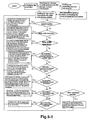
- the software flow charts are shown in Fig. 4-1 or Fig. 4-2.
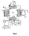
- the controller module 1 uses a private processor chip U3 that is the microprocessor capable of controlling the USB interface.
- XT1 is an 8MHz crystal oscillator.
- the firmware is provided in the controller module 1, more particularly, in the processor chip U3. Its main function is to perform the device control, data access, interface control and information prompt and the like of the semiconductor storage apparatus.
- the firmware is provided with the information prompt control program.
- This program and the information prompt control module 51 in the information prompt module 5 are used to detect, read, write and control the information content, prompt mode and the like prompted by the information prompt module 5, and to feedback the information of the information prompt module 5 to the data processing system.
- the information prompt control module 51 in the information prompt module 5 and the controller module 1 may be independent or combined together.
- Fig. 5-1 is a flow chart of the firmware with the function of the password protection
- Fig. 5-2 is a flow chart of the firmware without the function of the password protection.
- the power source module 4 realizes not only the direct-current 5V USBVCC supplied by USB of the data processing system, but also the direct-current POWER-5V supplied by the battery power source 44.
- the host power source USBVCC supplies power to the semiconductor storage apparatus through the power source automatic switch circuit composed of R34, D1, Q1, R35, AAT4250 switching to USB interface power source.
- the battery power source POWER_5V supplies power to the semiconductor storage apparatus through the power source automatic switch circuit composed of the above elements switching to the battery power source.
- the direct-current 5V power source supplied by the above two modes is converted into 3.3V power source through the chip U4 and parallel connected capacitors C11, C12, C13, C14.
- the charge circuit composed of C17, C18, R38, LTC1734, Q2 in the power source 4 charges the battery power source 44 automatically after the semiconductor storage apparatus is connected with the data processing system to ensure the normal power supply of the battery power source 44 under the supply mode of the battery power source.
- the liquid crystal display component 54 uses a 128 ⁇ 32 dot matrix character type liquid crystal display, as shown in Fig. 13.
- the liquid crystal display component comprises a liquid crystal module (LCM) and a liquid crystal control module (MPU).
- the liquid crystal control module (MPU) receives the control signal from the microprocessor U3, and controls the information of the liquid crystal module (LCM) to display according to the control signal.
- Fig. 13 is a schematic circuit diagram of the connection circuit between the liquid crystal display (LCD) and the controller 1, wherein LDB0 ⁇ LDB7 perform the data transmission, and connect with the corresponding LDB0 ⁇ LDB7 of the microprocessor U3 in Fig. 8.
- LCS port connects with the LCS port of the U3 to receive the selected signal for the LCD from the microprocessor U3, and to make the LCD under the ready state.
- REST as the reset port
- LR/W as the read-write signal port
- LD/I as the data command selection port
- LE as the enabling operation port connect, respectively, with the corresponding REST, LR/W, LD/I, LE ports of the microprocessor U3 in Fig.8.
- the microprocessor U3 controls the information display of the liquid crystal display, and the feedback information from the displayed information.
- the type of the liquid crystal display screen may be character type, graphic type, customized type or any other type.
- the type of the liquid crystal may be the character type liquid crystal or the dot matrix liquid crystal.
- the semiconductor storage apparatus gets driven by the battery power source, and the controller module 1 is initialized, that is, runs the firmware in the microprocessor chip U3.
- the firmware detects and obtains the capacitor, free space and other information of the storage medium module 3, including the device information, user's information (user's name, code, etc.), the stored information content, the date and the time, etc. of the information prompt storage region 31, and converts the above-mentioned information into the special control command to transmit it to the liquid crystal display (LCD) module.
- the liquid crystal module displays the above-mentioned information.
- the above-mentioned information cannot be completely displayed at once due to the limitation of the size of the liquid crystal module (LCM) 52, and thus the dynamic display can be set or the manual control display is performed by the manual control component 53 (e. g. button, switch, etc.) of the semiconductor storage apparatus. Then, the user or possessor can know clearly of the above-mentioned information of the semiconductor storage apparatus. Certainly, the user can also cut off the battery power source switch 43 to switch off the power source, and turn off the display to save the battery power source.
- the manual control component 53 e. g. button, switch, etc.
- a fixed or removable storage disk occurs in the data processing system host, and can be used as a hard disk or a floppy disk.
- the firmware of the processor chip U3 of the controller module 1 is activated, and initialized.
- the above-mentioned information is defined and displayed on the liquid crystal module (LCM) 52, and if necessary the read-write state information of the data (for instance, the read-write state information is "idle” or “waiting” here) is displayed thereon.
- the controller module 1 feedbacks the initialized information and the driver of the semiconductor storage apparatus to the host operation system through the USB interface, and the operation system performs the corresponding operation according to different feedback information or the property state.
- the firmware After the initialization of the firmware, it detects first the manufacturer and the product type information of the storage medium chip of the semiconductor storage medium module, calculates the total capacity of the storage disk, and then reads out FAT table in the storage disk, calculates the used space and the free space, and then reads the contents in the prompt information storage region, including but not limited to the manufacturer information, the user's name, the user's code, the user's password, the product type, the product serial number, the product barcode, the description of the storage content, etc. Then, the acquired information is displayed on the liquid crystal module in accordance with the predetermined format. After the above-mentioned steps, the firmware in the controller module 1 enters the waiting state immediately to wait for the operation request from the host.
- the data processing system sends the operation request of the universal interface to the storage apparatus through the driver, and the firmware in the apparatus processes the received standard operation request of the universal interface, and returns the result or state information to the data processing system.
- an information exchange path is established between the data processing system and the apparatus.
- the host operation system When the host operation system requests the read operation for the data, it will send the operation command to the driver; and the driver packages the read operation command via USB, and sends it to the firmware in the controller module 1 through the operation system.
- the firmware performs the read operation, that is, the firmware converts the logical address in the read command into the physical address in the semiconductor storage medium module 3, reads the data from the semiconductor storage medium according to the physical address and returns it to the data processing system. At the same time, it implements the information simultaneously prompt of the read operation state using LED indication lamp and the liquid crystal module 52, if necessary, to finish the read operation.
- the host operation system When the host operation system requests the write operation for the data, it will send the write operation command to the driver; and the driver packages the write operation command via USB, sends it to the firmware in the controller module 1 through the operation system.
- the firmware performs the read operation, that is, the firmware converts the logical address in the write command into the physical address in the semiconductor storage medium module 3, receives the data from the data processing system and writes the data into the semiconductor storage medium according to the physical address, and the driver returns the perform state information of the write operation to the operation system, and implements simultaneously the information prompt of the write operation state using LED indication lamp and the liquid crystal module 52, if necessary, to finish the write operation.
- the firmware also supports the command request for the password verification of the prompt information storage region.
- the firmware receives the password that the host requests to be verified from the universal interface, and reads the password from the prompt information storage region, and then compares them. If they are the same, the password verification is passed; otherwise, it fails. Then, the firmware returns the verified result to the data processing system through the universal interface.
- the firmware also supports the command request for setting up the password of the prompt information storage region.
- the firmware receives the password that the host requests to be set from the universal interface, and determines whether or not the password verification is passed. If passed, the new password is written into the prompt information storage region; otherwise, the modification is rejected. Then, the firmware returns the modified result to the data processing system through the universal interface.
- the firmware also supports the command request for writing the prompt information storage region, and the firmware receives the information that the host requests to be written into the prompt information storage region, and then determines whether or not the password verification is passed. If passed, the new information will be written into the prompt information storage region; otherwise, the writing is rejected. Then, the firmware returns the result to the data processing system through the universal interface.
- the firmware also supports the command request for reading the prompt information storage region, and the firmware determines whether or not the password verification is passed. If passed, it will read the data from the prompt information storage region and then send it into the host; otherwise, the reading is rejected. Then, the firmware returns the result to the data processing system through the universal interface.
- the firmware can receive the button information from the manual control component.
- the prompt information of different pages is displayed on LCD component according to the information of different buttons.
- the button can be combined with the power source switch.
- the content displayed on the LCD of the present invention can be defined and modified by the software for setting the prompt information storage region in the data processing system.
- the prompt information storage region can be protected by the password.
- the content of the prompt information storage region needs to be verified before being set or modified.
- the user can control the software with the information prompt setting in the data processing system to read and modify the manufacturer information, the user's name, the user's code, the user's password, the product type, the product serial number, the product barcode, the description of the storage content of the apparatus, and the display mode, display language, operation mode of the liquid crystal display apparatus, and the like.
- the defined or modified information is sent to the firmware of the controller module 1 by the data processing system through the USB interface.
- the firmware receives the password that the information prompt storage region needs to be verified from the host, and reads the original password from the semiconductor storage medium. If the legitimate verification is passed, the defined or modified prompt information will be received from the data processing system, and the data write operation will be performed.
- the new prompt information is written into the prompt information storage region, and meanwhile the firmware of the controller module 1 informs the information prompt module 5 to update the displayed information, and returns the performance situation of the data update operation and/or displayed prompt information to the data processing system.
- the flow chart of the software for setting the information prompt storage region is shown in Fig. 4-1.
- the software first receives the password inputted by the user, sends the password and the password verification request to the storage apparatus, and then reads the result of the password verification. If the verification fails several times, then the program ends. If the verification is passed, the content of the prompt information storage region can be read, modified, and set with a password.
- the program sends a request command for reading the content of the prompt information region to the storage apparatus, and then receives and processes the information returned from the apparatus, and displays the read content on the screen.
- the program receives the new prompt information content inputted by the user that needs to be set or modified, sends the written prompt information request and the new information prompt to be written to the storage apparatus, obtains the result processed by the apparatus, and displays the result on the screen.
- the program receives the new password inputted by the user, sends the password setting request and the new password to be set to the apparatus, and obtains the result processed by the apparatus, and displays the result on the screen.
- the content displayed by the liquid crystal display of the present invention can be defined and modified by the software for setting the prompt information store region running in the data processing system.
- the user can control the software for setting the prompt information storage region in the data processing system to read, and modify the manufacturer information, the user's name, the user's code, the product type, the product serial, the product bar code, the description of the storage content of the apparatus, and the display mode, the display language, the operation mode of the liquid crystal display apparatus, and the like.
- the defined or modified information is sent to the firmware of the controller module 1 by the data processing system through the USB interface.
- the firmware receives the defined or modified information prompt from the data processing system to write the data for writing the new prompt information into the prompt information storage region, and meanwhile the firmware of the controller module 1 informs the information prompt module 5 to update the displayed information, and returns the performance situation of the data update and/or the displayed prompt information to the data processing system.
- the flow chart of the software for setting up the prompt information storage region is shown in Fig. 4-2.
- the program When reading the content of the prompt information storage region, the program sends the request command for reading the content of the prompt information region to the storage apparatus, and then receives and processes the information returned from the apparatus, and displays the read content on the screen.
- the program receives the new prompt information inputted by the user that needs to be set or modified, sends the write request for the prompt information and the new prompt information to be written to the storage apparatus, obtains the result processed by the apparatus, and displays the result on the screen.
- the content stored in the prompt information region may be the character information and/or the pattern information; and the program can also convert the character information into the pattern information to store it in the prompt information storage region.
- the most preferable embodiment of the present invention is to use a microprocessor with the USB, a LCD module with the function of self-control, a flash memory and a USB interface.
- the LCD module may not have the function of self-control, and it is controlled by the microprocessor.
- the present invention may set the operation state of LED in addition to setting the LCD display module.
- the present invention is further designed with the data protection and data retrieval functions such that the data stored in the storage apparatus cannot be damaged even when the user cuts off the connection between the storage apparatus and the data processing system host, or the power lost or the death of the computer occurs suddenly during the data is being written into the storage apparatus, and the damage of the data being written can be minimized.
- the way to realize the above function may be: 1. first searching a free new block of data in the semiconductor storage medium when the data is written into the semiconductor storage medium, such as flash memory, then writing the data to be written into the new block of data, and possibly recording the logical address corresponding to the new block of data in the new block of data if necessary.
- the different writing states are marked, if necessary, for the data retrieval.
- the data retrieval can perform at the next power-up.
- the way to achieve the above function can also be: 2. storing the original block of data where the covered data is present into the buffer of the storage medium first, clearing the original block of data if necessary, writing the new data into the original block of data, and then copying the uncovered data of the original block of data from the buffer to the original block of data.
- the different writing states are marked, if necessary, for the data retrieval.
- the content obtained by the aforesaid way is displayed on the screen.
- the program receives the new prompt information inputted by the user that needs to be set or modified, sends the write request for the prompt information and the new prompt information to be written to the storage apparatus, obtains the result processed by the apparatus, and displays the result on the screen.
- the content stored in the prompt information region may be the character information and/or the pattern information; and the program can also convert the character information into the pattern information to store it in the prompt information storage region.
- the most preferable embodiment of the present invention is to use a microprocessor with USB function, a LCD display module with the self-control function, flash memory and USB interface. Moreover, the LCD display module may not have the self-control function, and its control function is realized by the microprocessor.
- the present invention may set the operation state of a LED in addition to setting the LCD display module.
- the present invention is further designed with the data protection and data retrieval functions such that the data stored in the storage apparatus cannot be damaged even when the user cuts off the connection between the storage apparatus and the data processing system host, or the power lost or the death of the computer occurs suddenly during the data is being written into the storage apparatus, and the damage of the data being written can be minimized.
- the way to realize the above function may be: 1. first searching a free new block of data in the semiconductor storage medium when the data is written into the semiconductor storage medium, such as flash memory, then writing the data to be written into the new block of data, and possibly recording the logical address corresponding to the new block of data in the new block of data if necessary.
- the different writing states are marked, if necessary, for the data retrieval.
- the data retrieval can perform at the next power-up.
- the way to achieve the above function can also be: 2. storing the original block of data where the covered data is present into the buffer of the storage medium first, clearing the original block of data if necessary, writing the new data into the original block of data, and then copying the uncovered data of the original block of data from the buffer to the original block of data.
- the different writing states are marked, if necessary, for the data retrieval.
- the data processing system referred to by the present invention comprises, but not limited to the computer, PDA, mobile telephone, MP3, digital camera, digital video, palm apparatus, etc.
Landscapes
- Engineering & Computer Science (AREA)
- Theoretical Computer Science (AREA)
- Computer Security & Cryptography (AREA)
- Computer Hardware Design (AREA)
- Physics & Mathematics (AREA)
- General Engineering & Computer Science (AREA)
- General Physics & Mathematics (AREA)
- Software Systems (AREA)
- Storage Device Security (AREA)
Applications Claiming Priority (3)
| Application Number | Priority Date | Filing Date | Title |
|---|---|---|---|
| CNB021342903A CN1270235C (zh) | 2002-06-30 | 2002-06-30 | 实现信息提示的半导体存储方法及装置 |
| CN02134290 | 2002-06-30 | ||
| PCT/CN2003/000021 WO2004003754A1 (en) | 2002-06-30 | 2003-01-13 | Semiconductor storage method and apparatus for implementing information prompt |
Publications (2)
| Publication Number | Publication Date |
|---|---|
| EP1533705A1 true EP1533705A1 (de) | 2005-05-25 |
| EP1533705A4 EP1533705A4 (de) | 2010-08-18 |
Family
ID=4747665
Family Applications (1)
| Application Number | Title | Priority Date | Filing Date |
|---|---|---|---|
| EP03702286A Withdrawn EP1533705A4 (de) | 2002-06-30 | 2003-01-13 | Halbleiterspeicherverfahren und vorrichtung zur implementierung einer informationsaufforderung |
Country Status (7)
| Country | Link |
|---|---|
| US (1) | US20050207241A1 (de) |
| EP (1) | EP1533705A4 (de) |
| JP (1) | JP2005531835A (de) |
| KR (1) | KR20050027227A (de) |
| CN (1) | CN1270235C (de) |
| AU (1) | AU2003207088A1 (de) |
| WO (1) | WO2004003754A1 (de) |
Families Citing this family (7)
| Publication number | Priority date | Publication date | Assignee | Title |
|---|---|---|---|---|
| JP5407816B2 (ja) * | 2009-01-07 | 2014-02-05 | セイコーエプソン株式会社 | 半導体記憶装置、及び、半導体記憶装置の制御方法 |
| CN102467464A (zh) * | 2010-11-11 | 2012-05-23 | 鸿富锦精密工业(深圳)有限公司 | 可移动存储设备盘符识别系统及方法 |
| CN102938659A (zh) * | 2012-10-19 | 2013-02-20 | 深圳桑菲消费通信有限公司 | 一种nfc套件及其实现方法 |
| CN104021810A (zh) * | 2013-02-28 | 2014-09-03 | 联想(北京)有限公司 | 可移动存储设备及用于其的方法 |
| CN103577124A (zh) * | 2013-11-15 | 2014-02-12 | 华为终端有限公司 | 一种提示外接存储设备读写状态的方法及设备 |
| CN113168851A (zh) * | 2020-07-13 | 2021-07-23 | 深圳市大疆创新科技有限公司 | 存储设备、信息处理方法和存储系统 |
| US12045473B2 (en) * | 2022-06-14 | 2024-07-23 | Western Digital Technologies, Inc. | Data storage device and method for prediction-based improved power-loss handling |
Family Cites Families (8)
| Publication number | Priority date | Publication date | Assignee | Title |
|---|---|---|---|---|
| EP0467208B1 (de) * | 1990-07-11 | 1995-09-20 | Hitachi, Ltd. | Digitales Informationssystem |
| US5892902A (en) * | 1996-09-05 | 1999-04-06 | Clark; Paul C. | Intelligent token protected system with network authentication |
| US6219439B1 (en) * | 1998-07-09 | 2001-04-17 | Paul M. Burger | Biometric authentication system |
| US7272723B1 (en) * | 1999-01-15 | 2007-09-18 | Safenet, Inc. | USB-compliant personal key with integral input and output devices |
| JP3389186B2 (ja) * | 1999-04-27 | 2003-03-24 | 松下電器産業株式会社 | 半導体メモリカード及び読み出し装置 |
| US7178031B1 (en) * | 1999-11-08 | 2007-02-13 | International Business Machines Corporation | Wireless security access management for a portable data storage cartridge |
| FI20001073A7 (fi) * | 2000-05-08 | 2001-11-09 | Nokia Corp | Menetelmä muistikortin suojaamiseksi ja muistikortti |
| JP2003256282A (ja) * | 2002-02-28 | 2003-09-10 | Matsushita Electric Ind Co Ltd | メモリカード |
-
2002
- 2002-06-30 CN CNB021342903A patent/CN1270235C/zh not_active Expired - Lifetime
-
2003
- 2003-01-13 EP EP03702286A patent/EP1533705A4/de not_active Withdrawn
- 2003-01-13 KR KR1020047021622A patent/KR20050027227A/ko not_active Ceased
- 2003-01-13 JP JP2004516415A patent/JP2005531835A/ja active Pending
- 2003-01-13 AU AU2003207088A patent/AU2003207088A1/en not_active Abandoned
- 2003-01-13 WO PCT/CN2003/000021 patent/WO2004003754A1/zh not_active Ceased
- 2003-01-13 US US10/519,437 patent/US20050207241A1/en not_active Abandoned
Also Published As
| Publication number | Publication date |
|---|---|
| JP2005531835A (ja) | 2005-10-20 |
| WO2004003754A1 (en) | 2004-01-08 |
| US20050207241A1 (en) | 2005-09-22 |
| CN1388447A (zh) | 2003-01-01 |
| CN1270235C (zh) | 2006-08-16 |
| KR20050027227A (ko) | 2005-03-18 |
| EP1533705A4 (de) | 2010-08-18 |
| AU2003207088A1 (en) | 2004-01-19 |
Similar Documents
| Publication | Publication Date | Title |
|---|---|---|
| US7587554B2 (en) | Device and method for providing data exchange and storage | |
| JP4551320B2 (ja) | 電子フラッシュ・メモリ式外部記憶方法及びその装置 | |
| US6795327B2 (en) | Semiconductor storage method and device supporting multi-interface | |
| KR100899511B1 (ko) | 컴퓨터 주변기기에 저장 기능을 부가하는 방법 및 그 구조 | |
| JP2003099184A (ja) | 情報処理システム、それに用いる情報処理装置および入力ペン | |
| CA2117065A1 (en) | Portable computer keyboard | |
| AU2011210339B2 (en) | USB memory device | |
| US20050207241A1 (en) | Semiconductor storage method and apparatus for implementing imormation prompt | |
| US20030074572A1 (en) | Battery enclosing encryption key | |
| US5974161A (en) | Detachable card for capturing graphics | |
| CN100440178C (zh) | 移动存储装置的盘符管理方法 | |
| TWI407327B (zh) | 資料處理方法、系統及儲存裝置控制器 | |
| CN100501634C (zh) | 数据处理装置 | |
| US20010017701A1 (en) | Peripheral device for information processing and information processing system | |
| KR100571887B1 (ko) | 휴대용 메모리 카드 백업장치 | |
| US20050116936A1 (en) | Touch pad for displaying information | |
| JPH08328683A (ja) | コンピュータシステム及びそのメッセージ表示方法 | |
| JP2001067226A (ja) | プログラムダウンロードシステム | |
| KR20030031527A (ko) | 홍보 기능을 갖는 휴대용 데이터 저장장치의 동작제어방법및 이를 수행하기 위한 시스템 | |
| JPH0728585A (ja) | スタイラスペンおよびそれを使用したペン入力型コンピュータ | |
| JP2006164137A (ja) | アクセス制御システム及びアクセス制御プログラム | |
| JP2005169862A (ja) | 画像形成装置 | |
| JP2716039B2 (ja) | 記憶装置 | |
| KR200337833Y1 (ko) | 휴대용 메모리 카드 백업장치 | |
| JPH11249885A (ja) | 書き換え制御システムおよび方法 |
Legal Events
| Date | Code | Title | Description |
|---|---|---|---|
| PUAI | Public reference made under article 153(3) epc to a published international application that has entered the european phase |
Free format text: ORIGINAL CODE: 0009012 |
|
| 17P | Request for examination filed |
Effective date: 20050125 |
|
| AK | Designated contracting states |
Kind code of ref document: A1 Designated state(s): AT BE BG CH CY CZ DE DK EE ES FI FR GB GR HU IE IT LI LU MC NL PT SE SI SK TR |
|
| AX | Request for extension of the european patent |
Extension state: AL LT LV MK RO |
|
| RAP1 | Party data changed (applicant data changed or rights of an application transferred) |
Owner name: NETAC TECHNOLOGY CO., LTD. |
|
| DAX | Request for extension of the european patent (deleted) | ||
| A4 | Supplementary search report drawn up and despatched |
Effective date: 20100719 |
|
| 17Q | First examination report despatched |
Effective date: 20101109 |
|
| STAA | Information on the status of an ep patent application or granted ep patent |
Free format text: STATUS: THE APPLICATION IS DEEMED TO BE WITHDRAWN |
|
| 18D | Application deemed to be withdrawn |
Effective date: 20110322 |