EP1530068A2 - Flacher faseroptischer Stecker - Google Patents
Flacher faseroptischer Stecker Download PDFInfo
- Publication number
- EP1530068A2 EP1530068A2 EP05075158A EP05075158A EP1530068A2 EP 1530068 A2 EP1530068 A2 EP 1530068A2 EP 05075158 A EP05075158 A EP 05075158A EP 05075158 A EP05075158 A EP 05075158A EP 1530068 A2 EP1530068 A2 EP 1530068A2
- Authority
- EP
- European Patent Office
- Prior art keywords
- fiber optic
- optic connector
- wafer
- ferrule
- door
- Prior art date
- Legal status (The legal status is an assumption and is not a legal conclusion. Google has not performed a legal analysis and makes no representation as to the accuracy of the status listed.)
- Withdrawn
Links
Images


Classifications
-
- G—PHYSICS
- G02—OPTICS
- G02B—OPTICAL ELEMENTS, SYSTEMS OR APPARATUS
- G02B6/00—Light guides; Structural details of arrangements comprising light guides and other optical elements, e.g. couplings
- G02B6/24—Coupling light guides
- G02B6/36—Mechanical coupling means
- G02B6/38—Mechanical coupling means having fibre to fibre mating means
- G02B6/3807—Dismountable connectors, i.e. comprising plugs
- G02B6/3833—Details of mounting fibres in ferrules; Assembly methods; Manufacture
- G02B6/3847—Details of mounting fibres in ferrules; Assembly methods; Manufacture with means preventing fibre end damage, e.g. recessed fibre surfaces
- G02B6/3849—Details of mounting fibres in ferrules; Assembly methods; Manufacture with means preventing fibre end damage, e.g. recessed fibre surfaces using mechanical protective elements, e.g. caps, hoods, sealing membranes
-
- G—PHYSICS
- G02—OPTICS
- G02B—OPTICAL ELEMENTS, SYSTEMS OR APPARATUS
- G02B6/00—Light guides; Structural details of arrangements comprising light guides and other optical elements, e.g. couplings
- G02B6/24—Coupling light guides
- G02B6/36—Mechanical coupling means
- G02B6/38—Mechanical coupling means having fibre to fibre mating means
- G02B6/3807—Dismountable connectors, i.e. comprising plugs
- G02B6/381—Dismountable connectors, i.e. comprising plugs of the ferrule type, e.g. fibre ends embedded in ferrules, connecting a pair of fibres
- G02B6/3818—Dismountable connectors, i.e. comprising plugs of the ferrule type, e.g. fibre ends embedded in ferrules, connecting a pair of fibres of a low-reflection-loss type
- G02B6/3821—Dismountable connectors, i.e. comprising plugs of the ferrule type, e.g. fibre ends embedded in ferrules, connecting a pair of fibres of a low-reflection-loss type with axial spring biasing or loading means
-
- G—PHYSICS
- G02—OPTICS
- G02B—OPTICAL ELEMENTS, SYSTEMS OR APPARATUS
- G02B6/00—Light guides; Structural details of arrangements comprising light guides and other optical elements, e.g. couplings
- G02B6/24—Coupling light guides
- G02B6/36—Mechanical coupling means
- G02B6/38—Mechanical coupling means having fibre to fibre mating means
- G02B6/3807—Dismountable connectors, i.e. comprising plugs
- G02B6/3873—Connectors using guide surfaces for aligning ferrule ends, e.g. tubes, sleeves, V-grooves, rods, pins, balls
- G02B6/3874—Connectors using guide surfaces for aligning ferrule ends, e.g. tubes, sleeves, V-grooves, rods, pins, balls using tubes, sleeves to align ferrules
- G02B6/3878—Connectors using guide surfaces for aligning ferrule ends, e.g. tubes, sleeves, V-grooves, rods, pins, balls using tubes, sleeves to align ferrules comprising a plurality of ferrules, branching and break-out means
- G02B6/3879—Linking of individual connector plugs to an overconnector, e.g. using clamps, clips, common housings comprising several individual connector plugs
-
- G—PHYSICS
- G02—OPTICS
- G02B—OPTICAL ELEMENTS, SYSTEMS OR APPARATUS
- G02B6/00—Light guides; Structural details of arrangements comprising light guides and other optical elements, e.g. couplings
- G02B6/24—Coupling light guides
- G02B6/36—Mechanical coupling means
- G02B6/38—Mechanical coupling means having fibre to fibre mating means
- G02B6/3807—Dismountable connectors, i.e. comprising plugs
- G02B6/3897—Connectors fixed to housings, casing, frames or circuit boards
-
- G—PHYSICS
- G02—OPTICS
- G02B—OPTICAL ELEMENTS, SYSTEMS OR APPARATUS
- G02B6/00—Light guides; Structural details of arrangements comprising light guides and other optical elements, e.g. couplings
- G02B6/24—Coupling light guides
- G02B6/36—Mechanical coupling means
- G02B6/38—Mechanical coupling means having fibre to fibre mating means
- G02B6/3807—Dismountable connectors, i.e. comprising plugs
- G02B6/3873—Connectors using guide surfaces for aligning ferrule ends, e.g. tubes, sleeves, V-grooves, rods, pins, balls
- G02B6/3882—Connectors using guide surfaces for aligning ferrule ends, e.g. tubes, sleeves, V-grooves, rods, pins, balls using rods, pins or balls to align a pair of ferrule ends
-
- G—PHYSICS
- G02—OPTICS
- G02B—OPTICAL ELEMENTS, SYSTEMS OR APPARATUS
- G02B6/00—Light guides; Structural details of arrangements comprising light guides and other optical elements, e.g. couplings
- G02B6/24—Coupling light guides
- G02B6/36—Mechanical coupling means
- G02B6/38—Mechanical coupling means having fibre to fibre mating means
- G02B6/3807—Dismountable connectors, i.e. comprising plugs
- G02B6/3873—Connectors using guide surfaces for aligning ferrule ends, e.g. tubes, sleeves, V-grooves, rods, pins, balls
- G02B6/3885—Multicore or multichannel optical connectors, i.e. one single ferrule containing more than one fibre, e.g. ribbon type
Definitions
- PCB printed circuit boards
- a traditional backplane is a printed circuit board that has many signal traces running through it.
- the traces route signals between electrical connectors mounted on a surface of the backplane.
- the daughter cards have mating electrical connectors along one edge, allowing each daughter card to be plugged into the backplane. In this configuration, the daughter cards are parallel to each other and mounted typically at right angles to the backplane.
- optical communications is not like electronic communications.
- Light is an electromagnetic radiation having unique characteristics that are different from the characteristics of electrons. Therefore, designing a backplane assembly for light transmission has different considerations from designing a backplane assembly for electronic transmission.
- a backplane assembly designed for light transmission generally includes connectors that have a ferrule holding a single optical fiber or a multi-fiber optical ribbon.
- the ferrule on the daughter card connector is mated with a corresponding ferrule on the backplane connector so that the optical fibers held in the mating ferrules are aligned to minimize loss.
- These ferrules are conventionally placed in the mating position by alignment pins and passages for receiving the alignment pins.
- optical fibers Due to the size of the optical fibers utilized, for example 125 micron (10 -6 meter) diameter with a 62.5 micron diameter core, it is critical to maintain precise tolerances with the alignment pins and the receiving passages. Failure to maintain precise tolerances and any other misalignment/defect could lead to significant loss of data signals at the fiber-to-fiber interface.
- wipe length refers to the distance required for the electrical connectors on the daughter card and backplane to establish electrical engagement.
- the electrical connectors are mounted on the edge of the daughter card often near the optical connectors.
- This "wipe” is required primarily to counteract accumulated tolerances within the backplane/daughter card enclosure.
- Factors such as PCB uniformity, planarity, positional tolerancing, PCB lock location, component tolerancing and connector binding, all play roles in the final position of the electrical connectors in relation to the PCBs. These same factors can be detrimental to fiber optic connectors.
- Fiber optic connectors function as butt-coupled devices. The end faces holding the optical fibers must remain in physical contact at all times to ensure that the optical signals traveling in the optical fibers are stable and uninterrupted. Therefore, fiber optic connectors must be designed to establish full engagement and provide "float" (movability in the axis of engagement) to accommodate the variable wipe of the electrical connectors. There are two main reasons for this.
- mating forces in excess of 150 lbs. can be generated when joining high-density electrical connectors.
- Manual cam latch mechanisms are conventionally used to join the individual daughter cards to the backplane. These mechanisms, although manually operated, do not provide much user feedback other than a go or no-go type situation. With this being the case, if any connector is not properly aligned under such loads, then there is a strong likelihood of problems for the connection system. Therefore, it is critical that individual connectors are aligned before the latches are engaged. Furthermore, it is desirable to isolate mating force spikes by staggering the mating sequence from optical to electrical. This will provide for smoother cam latch activation when attempting to seat the daughter card on the backplane. Also, any additional loads that could bring the latches beyond their elastic limit are removed.
- a slidable mechanism is typically employed within the system.
- a prior art system disclosed in U.S. Patent No. 5,121,454 issued to Iwano et al. utilizes side latches incorporated into the connector housing for mating, and the configuration of the latches and the connector housing provide float in the Z-direction.
- the latching approach of the prior art '454 patent is described in more detail with respect to FIG. 1 in the Detailed Description section.
- Another object of the invention is to provide a fiber optic connector design that permits modularity for flexible configurations to meet various system configurations and/or density requirements.
- Still another object of the invention is to provide a fiber optic connector design that improves cost, process control and manufacturing lead time.
- Yet another object of the invention is to provide a fiber optic connector design that improves cleanliness and component protection while also providing eye safety.
- a fiber optic connector having at least one wafer, wherein the wafer holds at least one optical fiber.
- the wafer includes a retractable shroud, a body to receive the retractable shroud, and at least one biasing member.
- the biasing member is capable of being biased when the wafer contacts a corresponding mating wafer to cause the shroud to retract.
- the wafer as stated further includes the retractable shroud having a door that preferably opens outwardly and at least one ferrule that holds the optical fiber, where the ferrule is provided with an alignment pin.
- the biasing member includes a first biasing member, a second biasing member and a third biasing member.
- the first biasing member is capable of being biased to cause the alignment pin of the ferrule to open the door of the retractable shroud.
- the second biasing member is capable of being biased to cause the retractable shroud to be received by the body.
- the third biasing member is capable of being biased to cause the retractable shroud and the body to accommodate variable wipe length.
- Figure 1 illustrates three different configurations for a fiber optic connection system.
- Options 1 and 3 are configurations of the prior art, while option 2 is the configuration of the present invention.
- FIG. 1 shows the forces that exist due to the latching configuration utilized. The loops represent the circle of force and how it is distributed in the system, while the bold arrow identifies whether or not a forward force will be applied to the backplane after mating. Note that only in the configuration of option 1, is there a forward force applied to the backplane after mating. Latches are solidly colored for easier identification.
- Option 1 shows a prior art daughter card fiber optic connector that is rigidly held to the backplane by external cam latches or card screw mounted in the enclosure.
- This configuration is utilized, for example, by 3M's OGI backplane connector.
- the force is distributed throughout the daughter card and is putting pressure on the retention means (e.g., latch or screws) in an attempt to force the daughter card back out of the system.
- Float in the axis of engagement is provided by springs loaded to an adapter (not shown) attached to the connector.
- This option is viable when the daughter card is relatively small.
- option 1 has disadvantages that make this option undesirable in many circumstances. For example, when the daughter card is no longer small, forces distributed over such distance would be difficult to control and predict. Also, when many ferrules are required for each connector, the force required increases and is multiplied by the number of daughter cards. Further, this configuration does not lend itself to a wide variety of system configurations.
- Option 3 shows a prior art daughter card fiber optic connector in which the forces arc removed from the backplane once the system is fully engaged.
- This configuration is desirable from the standpoint that because the force on the backplane has been removed, there is eliminated the potential for fatigue in the system or stresses which may damage electrical components.
- the side latches typically made of plastic, retain the two assembly halves together, and allow the connector on either the daughter card or the backplane to float in the Z-direction (axis of engagement).
- the fiber optic connector of option 3 is undesirable from the standpoint that it lacks design flexibility and uses up valuable space on a printed circuit board.
- the fiber optic connector configuration shown in option 2 which is the preferred embodiment of the present invention, utilizes separable wafer modules.
- the configuration of option 2 preferably utilizes separable latching modules.
- This approach provides an opportunity for stackable components, which act as modular building blocks.
- modular latching provides an ability to distribute forces within a system as desired. By simply adding another latching module into the connector assembly, loads can be distributed over a greater surface area and thus, minimize the force on any given latching module.
- metallic materials may be used if desired to encapsulate the connector, thereby improving the overall system's shielding and durability.
- custom designs can be configured without specialty tooling and assembly equipment, thereby providing a vehicle for fast, cost-effective manufacturing cycles and scalability.
- the position of the latching modules shown in option 2 is solely for illustrative purposes and is in no way intended to limit the scope of the present invention to the configuration shown therein.
- FIG. 2 is a perspective view showing an embodiment of a fiber optic connector assembly configuration (in an unmated position) of option 2 of FIG. 1, generally shown by reference numeral 10, along with an electrical connector assembly (in an unmated position), generally shown by reference numeral 90.
- Fiber optic connectors of the fiber optic connector assembly 10 and electrical connectors of the electrical connector assembly 90 are attached to first and second printed circuit boards ("PCB") 21 and 22.
- FIG. 3 is a perspective view showing only the fiber optic connector assembly 10 of FIG. 2.
- the objects of the present invention may be achieved with one, two or more fiber optic connectors attached to each PCB 21, 22.
- the fiber optic connector assembly 10 includes the fiber optic connector 20 for the first PCB 21, e.g., backplane, and the mating fiber optic connector 30 for the second PCB 22, e.g., a daughter card.
- the fiber optic connector 20 includes a plurality of wafers 23, latching modules 26, and a module carrier 27, preferably a stiffening member, which holds the wafers 23 and the latching modules 26.
- the fiber optic connector 30 includes a plurality of wafers 34, latching modules 35, and a module carrier 37, preferably a stiffening member, which holds the wafers 34 and the latching modules 35. While the latching modules 26 are shown with fiber optic connector 20 and the latching modules 35 shown with fiber optic connector 30, it should be apparent to one of ordinary skill in the art that the location of the modules 26, 35 may be exchanged without deviating from the function or objectives of the present invention.
- the design of the fiber optic connectors 20, 30 allows for modularity because the wafers are similarly sized. This means that accommodating different system configurations or density requirements can be achieved by selecting a suitable stiffening member and number of wafers as desired. Note that the latching modules 26, 35 are also modular, so the number of such modules incorporated and the location of such modules on the fiber optic connectors can be varied.
- FIGS. 4 and 5 show one of the plurality of wafers 34 of the fiber optic connector 30 of FIGS. 2 and 3.
- the wafer 34 includes a support frame 46, a body 40 and a retractable shroud 41.
- the support frame 46 is configured to be attachable to the stiffening member 37.
- the retractable shroud 41 has a door 42 that preferably opens outwardly. In FIG. 4, the door 42 is shown in the closed position and in FIG. 5, the door 42 is shown in the opened position.
- At least one ferrule 44 (shown in FIG. 5) for holding one or more optical fibers 32 is housed in the retractable shroud 41/body 40 of the wafer 34.
- the ferrule 44 may be one of the commercially available ferrules, such as, for example, the MT ("Mechanical Transfer") ferrule developed by Nippon Telegraph and Telephone Corporation or the MAC ("Multifiber Array Connector”) ferrule developed by AT&T, or the ferrule disclosed in the concurrently filed non-provisional patent application entitled "Optical Connector Ferrule Designed To Minimize Manufacturing Imperfections And Mating Misalignments By Incorporating Exact Constraint Principles” (which is incorporated by reference herein), or any other ferrules that can be incorporated into the wafer design as described herein.
- the wafer 34 further includes an alignment pin 31 used to guide and align during mating of the ferrule 44 to a corresponding ferrule of wafer 23 of the fiber optic connector 20.
- the alignment pin 31 is used to open the door 42, thus protecting the ferrule from possible damage or wear while preventing the optical end face of the ferrule from coming into contact with possible debris or contaminants.
- the door 42 opens outwardly in the preferred embodiment, the door moves dirt, dust and other undesirable debris and contaminants away from the ferrule, where such debris and contaminants may interfere with transmission of optical data.
- Another advantage of the retractable shroud 41 design as shown in FIGS. 4 and 5 is that the door 42 does not open to expose the optical fibers 32 until wafers 34, 23 are mating. This is described in greater detail below.
- the embodiment described utilizes the alignment pin 31 to push open the door 42
- the door may be opened by an actuable member on the outside of the shroud which is actuated when contacted by the shroud of the opposing wafer.
- the preferred embodiment is a retractable shroud with an externally opening door
- the present invention can also function with an internally opening door.
- a pair of spring members 53 are shown between the body 40 and the support frame 46.
- the wafer 34 also has two other pairs of spring members 51, 52, which are shown in FIGS. 6a-6e. The operation of these spring members and the operation of the different components of the wafer 34 during mating of the wafer 34 to a corresponding wafer 23 are described with respect to FIGS. 6a-6e.
- FIGS. 6a-6e are not-to-scale drawings of the wafers 23, 34, intended only to illustrate the operation of the wafers 23, 34 during different stages of the mating process.
- FIG. 6a shows the wafers 23, 34 before the mating process has begun.
- Wafer 23 includes a body 60 and a retractable shroud 61.
- the body 60 is configured to be attachable to the stiffening member 27 (shown in FIGS. 2 and 3).
- the retractable shroud has a door 62 that opens outwardly.
- a ferrule 64 for holding one or more optical fibers (not shown) is housed in the retractable shroud 61/body 60 of the wafer 23.
- the ferrule 64 may be one of the commercially available ferrules, such as the MT-type or the MAC-type ferrule, or the ferrule disclosed in the concurrently filed non-provisional patent application entitled "Optical Connector Ferrule Designed To Minimize Manufacturing Imperfections And Mating Misalignments By Incorporating Exact Constraint Principles", or any other ferrules that can be incorporated into the wafer design as described herein.
- the wafer 23 further includes an alignment pin 71 used to guide and align during mating of the ferrule 64 to the corresponding ferrule 44 of wafer 34 of the fiber optic connector 30.
- the alignment pin 71 is used to push open the door 62, thus protecting the ferrule from possible damage or wear while preventing the optical end face of the ferrule from coming into contact with possible debris or contaminants.
- the door 62 opens outwardly, the door moves dirt, dust and other undesirable debris and contaminants away from the ferrule, where such debris and contaminants may interfere with transmission of optical data.
- Another advantage of the retractable shroud 61 design is that the door 62 does not open to expose the optical fibers until wafers 23, 34 are mating. Therefore, this design ensures eye safety.
- the wafer 23 also includes two pairs of spring members 81, 82.
- the embodiment described utilizes the alignment pin 71 to push open the door 62, it will be apparent to one of ordinary skill in the art that other ways to push open the door 62 may be utilized without departing from the function or objectives of the present invention.
- the door may be opened by an actuable member on the outside of the shroud which is actuated when contacted by the shroud of the opposing wafer.
- FIG. 6a shows the wafers 23, 34 before the mating process has begun. All of the pairs of spring members 51, 52, 53 of wafer 34 and the pairs of spring members 81, 82 of wafer 23 are in a preloaded state.
- the spring members 51 provide a spring rate K s
- the spring members 52 provide a spring rate K f
- the spring members 53 provide a spring rate K w .
- the spring members 81 provide a spring rate K a and the spring members 82 provide a spring rate K b .
- the spring rates and preloads of springs 51 and 81 are identical, and the spring rates and preloads of springs 52 and 82 are identical.
- the operation of the springs 81, 82 in wafer 23 will mirror the operation of the springs 51, 52 in wafer 34.
- the spring members 51, 52, 53, 81, 82 are shown as pairs of coiled springs.
- anything that is capable of providing a biasing force e.g., magnets, elastic materials
- the spring rates will be treated as one value for each pair of springs. The sequence of operation will now be described with reference to FIGS. 6b-6f.
- FIG. 6b shows the wafers 23, 34 at the moment of contact.
- the springs 51, 81 begin to compress as the preload force is overcome.
- FIG. 6f which is a diagram illustrating force of the springs of wafers 23, 34 and displacement of components of wafers 23, 34 during mating, shows the preload force of springs 51, 81 by reference numeral 94.
- the doors 42, 62 are in a closed position protecting the ferrules 44, 64 from debris and other contaminants.
- torsion springs 43, 63 generally bias the doors 42, 62, respectively, to a closed position; thus, forming a sealed chamber protected from debris and other contaminants.
- the increasing force applied thereon causes the ferrules 44, 64 to come into contact. This is shown in FIG. 6c.
- the displacement of the shrouds 41, 61 where the ferrules 44, 64 come into contact is shown in FIG. 6f by reference numeral 98, and the force required is indicated by reference numeral 105.
- the preload force of springs 52, 82 is indicated by reference numeral 93. As the preload force 93 of springs 52, 82 is overcome, the springs 52, 82 begin to compress and the ferrules 44, 64 and the shrouds 41,61 move in parallel at the combined spring rate K s + K f and K a + K b , respectively.
- the fiber optic connection system is configured so that the shrouds 41, 61 bottom out against the bodies 40, 60, respectively, as shown in FIG. 6d.
- the shroud displacement is indicated by reference numeral 100 (see FIG. 6f)
- the ferrule displacement is indicated by reference numeral 99
- the force required to reach this point is indicated by reference numeral 92
- the butt-couple force between the mated ferrules 44, 64 is indicated by reference numeral 103. Because the ferrules 44, 64 cannot be displaced any more, the force on the ferrules is held constant at the required butt-couple force for the remainder of the operations.
- the fiber optic connector design of the present invention accommodates variable wipe length of the electrical connectors, while minimizing potential optical fiber misalignment, and isolates the inner ferrule forces from the outer assembly.
- the movement of the fiber optic connector can be sequenced to ensure that the appropriate spring members are traveling when desired without the need for isolating faces or positive stops.
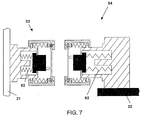
- FIG. 7 is a not-to-scale drawing of the wafers of an alternate embodiment of the fiber optic connector assembly of the present invention.
- the wafer 23 of the fiber optic connector 20 attached to the first PCB 21 is the same as in FIG. 6a.
- the wafer 84 of the fiber optic connector attached to the second PCB 22 is different from the wafer 34 in FIG. 6a.
- this wafer 84 does not have the pair of spring members 53 found in wafer 34.
- this wafer 84 is generally similar to the wafer 23 in configuration and operation; however, spring members 92 are longer than the spring members 82 of wafer 23 to provide float in the axis of engagement. While the fiber optic connector assembly shown in FIG. 7 may be suitable in certain cases, it will in other instances be inappropriate because of its limited ability to accommodate wide-ranging variable wipe length.
Landscapes
- Physics & Mathematics (AREA)
- General Physics & Mathematics (AREA)
- Optics & Photonics (AREA)
- Mechanical Coupling Of Light Guides (AREA)
- Optical Couplings Of Light Guides (AREA)
Applications Claiming Priority (5)
| Application Number | Priority Date | Filing Date | Title |
|---|---|---|---|
| US31659401P | 2001-08-31 | 2001-08-31 | |
| US316594P | 2001-08-31 | ||
| US196075 | 2002-07-16 | ||
| US10/196,075 US6769814B2 (en) | 2001-08-31 | 2002-07-16 | Waferized fiber optic connector |
| EP02768756A EP1421426B1 (de) | 2001-08-31 | 2002-08-29 | Flacher faseroptischer stecker |
Related Parent Applications (1)
| Application Number | Title | Priority Date | Filing Date |
|---|---|---|---|
| EP02768756A Division EP1421426B1 (de) | 2001-08-31 | 2002-08-29 | Flacher faseroptischer stecker |
Publications (2)
| Publication Number | Publication Date |
|---|---|
| EP1530068A2 true EP1530068A2 (de) | 2005-05-11 |
| EP1530068A3 EP1530068A3 (de) | 2005-11-30 |
Family
ID=34437545
Family Applications (1)
| Application Number | Title | Priority Date | Filing Date |
|---|---|---|---|
| EP05075158A Withdrawn EP1530068A3 (de) | 2001-08-31 | 2002-08-29 | Flacher faseroptischer Stecker |
Country Status (1)
| Country | Link |
|---|---|
| EP (1) | EP1530068A3 (de) |
Cited By (2)
| Publication number | Priority date | Publication date | Assignee | Title |
|---|---|---|---|---|
| WO2017102517A1 (en) * | 2015-12-14 | 2017-06-22 | Huber+Suhner Ag | Optical connector assembly |
| EP3182181A3 (de) * | 2015-11-24 | 2017-08-23 | Corning Optical Communications LLC | Optische rückwandverbinder und optische verbindungen damit |
Family Cites Families (4)
| Publication number | Priority date | Publication date | Assignee | Title |
|---|---|---|---|---|
| GB2124793B (en) * | 1982-07-24 | 1985-10-23 | Thorn Emi Electrical Component | Fibre optic connector |
| US5080461A (en) * | 1990-10-31 | 1992-01-14 | At&T Bell Laboratories | Retracting optical fiber connector |
| US5379362A (en) * | 1993-02-24 | 1995-01-03 | Sumitomo Wiring Systems, Ltd. | Optical fiber connector |
| DE59713003D1 (de) * | 1997-11-13 | 2009-06-04 | Diamond Sa | Steckeranordnung für eine optische Einschub-Steckverbindung |
-
2002
- 2002-08-29 EP EP05075158A patent/EP1530068A3/de not_active Withdrawn
Cited By (3)
| Publication number | Priority date | Publication date | Assignee | Title |
|---|---|---|---|---|
| EP3182181A3 (de) * | 2015-11-24 | 2017-08-23 | Corning Optical Communications LLC | Optische rückwandverbinder und optische verbindungen damit |
| US10353157B2 (en) | 2015-11-24 | 2019-07-16 | Corning Optical Communications, Llc | Backplane optical connectors and optical connections incorporating the same |
| WO2017102517A1 (en) * | 2015-12-14 | 2017-06-22 | Huber+Suhner Ag | Optical connector assembly |
Also Published As
| Publication number | Publication date |
|---|---|
| EP1530068A3 (de) | 2005-11-30 |
Similar Documents
| Publication | Publication Date | Title |
|---|---|---|
| US6769814B2 (en) | Waferized fiber optic connector | |
| US7073953B2 (en) | Modular fiber optic connection system | |
| US11828989B2 (en) | Fiber optic connectors, fiber optic adapters and related fiber optic connection systems | |
| AU707686B2 (en) | Optical connector with immovable ferrule | |
| EP1537629B1 (de) | Techniken zum verbinden einer menge von verbindungselementen unter verwendung einer verbesserten riegelungsvorrichtung | |
| EP1315991B1 (de) | Elektrooptisches stecker modul | |
| JP3505237B2 (ja) | プラグ保持装置及びそれを使用するデュプレックス型光コネクタ | |
| US20060153504A1 (en) | Multi fiber optical interconnect system, with push-push type insertion/withdrawal mechanism, MT-type connector and shuttered adapter and method for using same | |
| US11635575B2 (en) | Retrofit optical fiber connector module | |
| EP3855225B1 (de) | Optisches verbindungssystem | |
| EP1530068A2 (de) | Flacher faseroptischer Stecker | |
| US20070190841A1 (en) | Optical connector system | |
| US7556436B2 (en) | Optical connector system | |
| WO2006076061A2 (en) | Multi fiber optical interconnect system, with push-push type insertion/withdrawal mechanism, mt-type connector and shuttered adapter and method for using same | |
| Abendschein et al. | Recent advances in fiber-optic backplane connectors | |
| WO2026019665A1 (en) | Adapter module for use with very small form factor fiber optic connectors |
Legal Events
| Date | Code | Title | Description |
|---|---|---|---|
| PUAI | Public reference made under article 153(3) epc to a published international application that has entered the european phase |
Free format text: ORIGINAL CODE: 0009012 |
|
| 17P | Request for examination filed |
Effective date: 20050215 |
|
| AC | Divisional application: reference to earlier application |
Ref document number: 1421426 Country of ref document: EP Kind code of ref document: P |
|
| AK | Designated contracting states |
Kind code of ref document: A2 Designated state(s): AT BE BG DE FR GB |
|
| PUAL | Search report despatched |
Free format text: ORIGINAL CODE: 0009013 |
|
| AK | Designated contracting states |
Kind code of ref document: A3 Designated state(s): AT BE BG DE FR GB |
|
| AKX | Designation fees paid |
Designated state(s): DE FR GB |
|
| 17Q | First examination report despatched |
Effective date: 20060803 |
|
| R17C | First examination report despatched (corrected) |
Effective date: 20080502 |
|
| RAP1 | Party data changed (applicant data changed or rights of an application transferred) |
Owner name: AMPHENOL CORPORATION |
|
| STAA | Information on the status of an ep patent application or granted ep patent |
Free format text: STATUS: THE APPLICATION IS DEEMED TO BE WITHDRAWN |
|
| 18D | Application deemed to be withdrawn |
Effective date: 20100302 |