EP1529327B1 - Apparatus and method for measurement of dynamic laser signals - Google Patents
Apparatus and method for measurement of dynamic laser signals Download PDFInfo
- Publication number
- EP1529327B1 EP1529327B1 EP03701250A EP03701250A EP1529327B1 EP 1529327 B1 EP1529327 B1 EP 1529327B1 EP 03701250 A EP03701250 A EP 03701250A EP 03701250 A EP03701250 A EP 03701250A EP 1529327 B1 EP1529327 B1 EP 1529327B1
- Authority
- EP
- European Patent Office
- Prior art keywords
- sample
- laser
- signal
- photodiode
- light output
- Prior art date
- Legal status (The legal status is an assumption and is not a legal conclusion. Google has not performed a legal analysis and makes no representation as to the accuracy of the status listed.)
- Expired - Lifetime
Links
- 238000000034 method Methods 0.000 title claims abstract description 38
- 238000005259 measurement Methods 0.000 title abstract description 17
- 230000004044 response Effects 0.000 claims description 37
- 239000003990 capacitor Substances 0.000 claims description 12
- 238000006243 chemical reaction Methods 0.000 claims description 11
- 230000008033 biological extinction Effects 0.000 claims description 9
- 230000003111 delayed effect Effects 0.000 claims 6
- 230000003139 buffering effect Effects 0.000 claims 1
- 230000008054 signal transmission Effects 0.000 abstract description 5
- 230000001360 synchronised effect Effects 0.000 abstract description 2
- 230000003287 optical effect Effects 0.000 description 26
- 230000005540 biological transmission Effects 0.000 description 18
- 230000008569 process Effects 0.000 description 15
- 230000007704 transition Effects 0.000 description 11
- 230000001934 delay Effects 0.000 description 9
- 238000004891 communication Methods 0.000 description 7
- 230000008901 benefit Effects 0.000 description 6
- 230000015556 catabolic process Effects 0.000 description 5
- 238000006731 degradation reaction Methods 0.000 description 5
- 238000010586 diagram Methods 0.000 description 5
- 230000000694 effects Effects 0.000 description 4
- 230000032683 aging Effects 0.000 description 3
- 238000013459 approach Methods 0.000 description 3
- 238000005516 engineering process Methods 0.000 description 3
- 230000001151 other effect Effects 0.000 description 3
- 239000000243 solution Substances 0.000 description 3
- 230000003679 aging effect Effects 0.000 description 2
- 230000002431 foraging effect Effects 0.000 description 2
- 238000012544 monitoring process Methods 0.000 description 2
- 238000005457 optimization Methods 0.000 description 2
- 238000005070 sampling Methods 0.000 description 2
- 230000002277 temperature effect Effects 0.000 description 2
- 230000036962 time dependent Effects 0.000 description 2
- 229910000577 Silicon-germanium Inorganic materials 0.000 description 1
- LEVVHYCKPQWKOP-UHFFFAOYSA-N [Si].[Ge] Chemical compound [Si].[Ge] LEVVHYCKPQWKOP-UHFFFAOYSA-N 0.000 description 1
- 230000001419 dependent effect Effects 0.000 description 1
- 238000001514 detection method Methods 0.000 description 1
- 230000006870 function Effects 0.000 description 1
- 238000002347 injection Methods 0.000 description 1
- 239000007924 injection Substances 0.000 description 1
- 238000012804 iterative process Methods 0.000 description 1
- 239000000463 material Substances 0.000 description 1
- 238000012986 modification Methods 0.000 description 1
- 230000004048 modification Effects 0.000 description 1
- 238000012360 testing method Methods 0.000 description 1
- 238000012546 transfer Methods 0.000 description 1
Images


Classifications
-
- H—ELECTRICITY
- H04—ELECTRIC COMMUNICATION TECHNIQUE
- H04B—TRANSMISSION
- H04B10/00—Transmission systems employing electromagnetic waves other than radio-waves, e.g. infrared, visible or ultraviolet light, or employing corpuscular radiation, e.g. quantum communication
- H04B10/50—Transmitters
- H04B10/564—Power control
-
- H—ELECTRICITY
- H01—ELECTRIC ELEMENTS
- H01S—DEVICES USING THE PROCESS OF LIGHT AMPLIFICATION BY STIMULATED EMISSION OF RADIATION [LASER] TO AMPLIFY OR GENERATE LIGHT; DEVICES USING STIMULATED EMISSION OF ELECTROMAGNETIC RADIATION IN WAVE RANGES OTHER THAN OPTICAL
- H01S5/00—Semiconductor lasers
- H01S5/06—Arrangements for controlling the laser output parameters, e.g. by operating on the active medium
- H01S5/068—Stabilisation of laser output parameters
- H01S5/0683—Stabilisation of laser output parameters by monitoring the optical output parameters
- H01S5/06832—Stabilising during amplitude modulation
-
- H—ELECTRICITY
- H01—ELECTRIC ELEMENTS
- H01S—DEVICES USING THE PROCESS OF LIGHT AMPLIFICATION BY STIMULATED EMISSION OF RADIATION [LASER] TO AMPLIFY OR GENERATE LIGHT; DEVICES USING STIMULATED EMISSION OF ELECTROMAGNETIC RADIATION IN WAVE RANGES OTHER THAN OPTICAL
- H01S5/00—Semiconductor lasers
- H01S5/06—Arrangements for controlling the laser output parameters, e.g. by operating on the active medium
- H01S5/068—Stabilisation of laser output parameters
- H01S5/0683—Stabilisation of laser output parameters by monitoring the optical output parameters
- H01S5/06835—Stabilising during pulse modulation or generation
-
- H—ELECTRICITY
- H04—ELECTRIC COMMUNICATION TECHNIQUE
- H04B—TRANSMISSION
- H04B10/00—Transmission systems employing electromagnetic waves other than radio-waves, e.g. infrared, visible or ultraviolet light, or employing corpuscular radiation, e.g. quantum communication
- H04B10/07—Arrangements for monitoring or testing transmission systems; Arrangements for fault measurement of transmission systems
- H04B10/075—Arrangements for monitoring or testing transmission systems; Arrangements for fault measurement of transmission systems using an in-service signal
- H04B10/077—Arrangements for monitoring or testing transmission systems; Arrangements for fault measurement of transmission systems using an in-service signal using a supervisory or additional signal
-
- H—ELECTRICITY
- H04—ELECTRIC COMMUNICATION TECHNIQUE
- H04B—TRANSMISSION
- H04B10/00—Transmission systems employing electromagnetic waves other than radio-waves, e.g. infrared, visible or ultraviolet light, or employing corpuscular radiation, e.g. quantum communication
- H04B10/07—Arrangements for monitoring or testing transmission systems; Arrangements for fault measurement of transmission systems
- H04B10/075—Arrangements for monitoring or testing transmission systems; Arrangements for fault measurement of transmission systems using an in-service signal
- H04B10/079—Arrangements for monitoring or testing transmission systems; Arrangements for fault measurement of transmission systems using an in-service signal using measurements of the data signal
- H04B10/0795—Performance monitoring; Measurement of transmission parameters
- H04B10/07955—Monitoring or measuring power
-
- H—ELECTRICITY
- H04—ELECTRIC COMMUNICATION TECHNIQUE
- H04B—TRANSMISSION
- H04B10/00—Transmission systems employing electromagnetic waves other than radio-waves, e.g. infrared, visible or ultraviolet light, or employing corpuscular radiation, e.g. quantum communication
- H04B10/50—Transmitters
- H04B10/501—Structural aspects
- H04B10/503—Laser transmitters
- H04B10/504—Laser transmitters using direct modulation
-
- H—ELECTRICITY
- H01—ELECTRIC ELEMENTS
- H01S—DEVICES USING THE PROCESS OF LIGHT AMPLIFICATION BY STIMULATED EMISSION OF RADIATION [LASER] TO AMPLIFY OR GENERATE LIGHT; DEVICES USING STIMULATED EMISSION OF ELECTROMAGNETIC RADIATION IN WAVE RANGES OTHER THAN OPTICAL
- H01S5/00—Semiconductor lasers
- H01S5/04—Processes or apparatus for excitation, e.g. pumping, e.g. by electron beams
- H01S5/042—Electrical excitation ; Circuits therefor
-
- H—ELECTRICITY
- H01—ELECTRIC ELEMENTS
- H01S—DEVICES USING THE PROCESS OF LIGHT AMPLIFICATION BY STIMULATED EMISSION OF RADIATION [LASER] TO AMPLIFY OR GENERATE LIGHT; DEVICES USING STIMULATED EMISSION OF ELECTROMAGNETIC RADIATION IN WAVE RANGES OTHER THAN OPTICAL
- H01S5/00—Semiconductor lasers
- H01S5/06—Arrangements for controlling the laser output parameters, e.g. by operating on the active medium
- H01S5/068—Stabilisation of laser output parameters
- H01S5/06808—Stabilisation of laser output parameters by monitoring the electrical laser parameters, e.g. voltage or current
-
- H—ELECTRICITY
- H01—ELECTRIC ELEMENTS
- H01S—DEVICES USING THE PROCESS OF LIGHT AMPLIFICATION BY STIMULATED EMISSION OF RADIATION [LASER] TO AMPLIFY OR GENERATE LIGHT; DEVICES USING STIMULATED EMISSION OF ELECTROMAGNETIC RADIATION IN WAVE RANGES OTHER THAN OPTICAL
- H01S5/00—Semiconductor lasers
- H01S5/06—Arrangements for controlling the laser output parameters, e.g. by operating on the active medium
- H01S5/068—Stabilisation of laser output parameters
- H01S5/06812—Stabilisation of laser output parameters by monitoring or fixing the threshold current or other specific points of the L-I or V-I characteristics
-
- H—ELECTRICITY
- H01—ELECTRIC ELEMENTS
- H01S—DEVICES USING THE PROCESS OF LIGHT AMPLIFICATION BY STIMULATED EMISSION OF RADIATION [LASER] TO AMPLIFY OR GENERATE LIGHT; DEVICES USING STIMULATED EMISSION OF ELECTROMAGNETIC RADIATION IN WAVE RANGES OTHER THAN OPTICAL
- H01S5/00—Semiconductor lasers
- H01S5/06—Arrangements for controlling the laser output parameters, e.g. by operating on the active medium
- H01S5/068—Stabilisation of laser output parameters
- H01S5/06825—Protecting the laser, e.g. during switch-on/off, detection of malfunctioning or degradation
Definitions
- the present invention relates to a circuit and method used to calibrate and compensate for laser performance in systems such as an optical communications links, medical diagnostic systems and any other system utilizing lasers. Performance compensation is achieved in a non-invasive manner without disruption of the laser signal transmission or other operating parameters of the laser.
- the Digital Controller (111) requires feedback information from light output (107).
- the control system is operational, obtaining feedback information becomes problematic since the light output (107) constantly changes depending on the Drive Signal (100) the system is transmitting. Thus any attempts to measure the light output (107) will encounter errors, which can render the feedback information unusable.
- the Drive Signal (100) needs to be maintained at a fixed power level in order for the system to produce a steady value of the Light Output (107) so that calibration adjustments can be made. This procedure disrupts the signal transmission and, because of this, the transmitter cannot send information over the optical communications channel while the calibration is carried out. Disruption in communication is contrary to the goals of high reliability and 100% up time in present systems.
- the Photodiode Sensor (109) operates as a band-limiting filter converting the response to a variety of waveforms as follows:
- the present invention provides a circuit and a method for calibrating the Light Output (107) of the laser without affecting the data transmission. This is consistent with goals of high reliability because at no time is the data transmission disrupted.
- the present system contains a laser output measurement circuit used in a laser control system (114).
- the circuits contain a photodiode sensor (200), sample and hold amplifier (202), IC with synchronizer and delay circuits (206), and an analog to digital converter (204).
- the circuits measure the laser light output (107) while the laser Module (106) transmits signals.
- the measurement circuit tracks and stores the laser light output (107) signal using a Photodiode Sensor (109) and with a Sample/hold (202).
- the methods calculate the value of the laser light output (107) from mathematical relationships, which correlate the light output (107) of the laser Module (106) to the current value of the drive signal (100).
- An advantage of this invention is that laser power amplitude can be calibrated without interrupting the flow of information transmission.
- Another advantage of this invention is that the system can utilize multiple types of output responses from the Photodiode Sensor with the utilization of the appropriate correlation algorithm.
- Another advantage of this invention is that the transmitter optical power can be continuously maintained at the optimal value to achieve the target Extinction Ratio, Bit Error Rate and analog signal level.
- Another advantage of this invention is that the laser can be compensated for degradation due to aging. Yet another advantage of this invention is that adjustments to account for temperature changes, aging and other effects are done only as needed and by the amount needed. This contributes to extending the life of the laser.
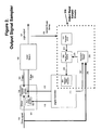
- FIG 1 a block diagram is shown for a Laser Control System (114).
- the system consists of a drive Signal Input (100) applied to a Laser Module Driver (101), which contains a Bias Current Generator (102) and a Modulation Current Generator (103).
- a Bias Control Signal (112) and a Modulation Control Signal (113) control the current generators.
- the Driver (101) produces Modulation Current (104) and Bias Current (105) that are applied to the Laser Module (106).
- the Laser Module (106) in turn produces Light Output (107).
- the magnitude of the Light Output (107) bears a relationship to the magnitude of the Modulation Current (104) and the Bias Current (105). A portion of the Light Output (107) from the laser is sensed.
- the Optical Power Sense (108), which is coupled to a Photodiode Sensor (109).
- the Photodiode Sensor Output (110) is connected to a Digital Controller (111).
- the Digital Controller (111) contains algorithms for laser control and also determines the magnitudes of the Bias Current Generator (102) and Modulation Current (103).
- FIG 2 shows the output signal sampler apparatus of this invention.
- This consists of a Photodiode Sensor (109), which generates a Photodiode Signal (201) in response to the application of a portion of the Laser Light Output (107).
- the Photodiode Output may be a fast response or an exponential rise and decay signal.
- the Sample and Hold Amplifier (202) receives the Photodiode Sensor Signal (201) and stores the value of the signal at the appropriate time as directed by the Sample and Hold Control (205). Once the Sample and Hold Amplifier (202) has stored the signal, it is sent to the Analog to Digital Converter (204), which is contained in the Digital Controller (111). The Sample and Hold Amplifier (202) is connected to the Analog to Digital Converter (204).
- the Sample and Hold Control (205) is produced by the Synchronizer and Delay Circuits (206). These circuits utilize real-time information of the state of the Drive Signal (100), which connects to the Drive Signal (100) at (208) in order to determine when the Sample and Hold Control (205) is activated.
- the Synchronizer and Delay Circuits (206) are controlled by the Digital Controller (111) with the necessary Logic Output (207).
- the Digital Controller (111) contains algorithms that are capable of utilizing a multiplicity of Photodiode Sensor information including an exponential rise and decay, a square wave response, and an average signal output. The algorithms utilize information related to the sequence of values of the Drive Signal (100) input and correlate those values to the magnitude of the Photodiode Sensor (109) output. In addition, the controller can then make adjustments to the Bias Current (105) and Modulation Current (104), in order to optimize the extinction ratio and the Bit Error Rate.
- FIG 3 is an embodiment of the Output Signal Sampler in this invention.
- the Drive Signal (100) applied to the Driver (103) produces a Light Output (107).
- a portion of the optical power is coupled to the Photodiode Sensor (109).
- the Photodiode Sensor (109) produces a current, which is converted to a voltage by the Transimpedance Amplifier (301).
- This voltage drives the Sample and Hold Amplifier (302), which in turn produces a steady sample of the sensor signal at (304) to the Analog to Digital Converter (304).
- the Sample and Hold Amplifier (202) stores the sensor information in a Capacitor C H (316).
- the capacitor is chosen so that the capturing of the sensor signal is done at high speed while at the same time the capacitor maintains the value of the captured sensor signal during the analog to digital conversion.
- the capacitor may need to be relatively small in the tens of picofarads in order for the Sample and Hold Amplifier (202) to successfully track the sensor signal.
- the Transimpedance Amplifier (301) and the Sample and Hold Amplifier (202) are designed in such a way that they will be substantially faster then the Photodiode Sensor (109) in order to insure that the Photodiode Sensor (109) determines the frequency response.
- a critical feature of the present invention is the appropriate timing of the Sample and Hold Control (205).
- This control must be able to capture the Photodiode Sensor (109) signal at a predictable time in order to anticipate the state of the Drive Signal (100) and the Light Output (107).
- the timing synchronization circuit determines this. This circuit starts by sampling the Drive Signal (100) at (315). This is done with the use of a Buffer (314) in order to avoid a significant load on the Drive Signal (100).
- the output of the Buffer (314) is sent to a set of n signal propagation delays. These delays consist of Delay 1 (312) to Delay n (313). These delays connect to Digital Multiplexer (309) through Inputs (310) to (311).
- the Digital Controller utilizes the Input Select (308) of the Digital Multiplexer (309) in order to select any of the n signal propagation delays.
- a zero to one transmission of the Drive Signal (100) will cause, after a time delay, a zero to one transition at the Set Input (307) of the Set Reset Latch (305).
- This transition in turn causes a zero to one transition of the Sample and Hold Control (205), which places the Sample and Hold Amplifier (202) in hold mode in order to prepare the system for an analog to digital conversion.
- the Set Reset Latch (305) is placed in reset mode by the Reset Signal (306) generated by the Digital Controller (111). This last step will then place the Sample and Hold Amplifier (202) in sample mode so that the system can be ready for the next calibration cycle.
- Figure 3 shows the propagation delays associated with the Output Signal Sampler. The following definitions apply:
- t Synch ( 415 ) t Drive 414 + t Sense 406 + t Capture 414
- the Analog to Digital Converter (204) performs an analog to digital conversion, which will last for a period of time t A/D (412).
- the duration of the analog to digital conversion can be relatively slow as required by the Analog to Digital Converter (204).
- the Digital Controller (111) will cause the S/H (408) signal to experience a Reset (412) transition to the sample mode with the use of the Reset Control (306).
- the embodiment shown in Figure 3 may utilize MOS technology components for a given data rate of transmission.
- Synchronization of the timing characteristics and delays as indicated by Equation 2 can be best achieved by including the Signal Sampler circuits of Figure 3 in the same integrated circuit as the Driver (103). If a single integrated circuit is not available, then the Signal Sampler circuits must be implemented with the appropriate technology in order to match the speed requirements of the propagation delays associated with the laser Driver (103). Very fast Silicon Germanium and other technologies are available. In some applications, fine-tuning and modifications of the embodiment of Figure 3 will be necessary to keep up with fast transmission rates. In these cases the same principles of the invention will apply and the task will consist of selecting the appropriate configuration of high-speed components.
- FIG 4 shows the timing of the in line calibration of the laser optical power.
- the system clock that is utilized by the transponder. This is the clock CLK (400).
- the clock (400) is utilized in the system to generate Serial Data Di (401).
- the Serial Data Di (401) consists of the sequence 101.
- the data transmission of the timing diagram in the illustration corresponds to NRZ-L.
- the Data flows through the Driver (103) and causes a zero to one transition in Laser Optical Power P L (403).
- This transition of the Laser Optical Power (403) happens after a delay t Drive (413), corresponding to the delay of the signal flowing through the Driver (103) and the Laser (106).
- a given setting of the Bias Current Generator (102) places the Laser (106) slightly above the threshold. This setting can be adjusted and controller independently from the signal modulation current.
- For the purpose of calibrating the Light Output (107) focus on the control of the Modulation Current Generator (103).
- the magnitude of the optical power is noted as Pmax (404).
- the laser optical power corresponding to the transmission of a logical 1 will vary depending on the setting of the Modulation Current Generator (103), the Laser (106) characteristics and the effects of factors such as temperature and aging on the Laser (106).
- the Photodiode Sample Hold Response V PS (405) will start sensing the Laser (106) output after a delay of t sense (406).
- the Sample and Hold Amplifier (202) will start increasing its voltage in an exponential manner reaching a maximum value Vpeak (407).
- High frequency models have been determined that demonstrate how the combination of amplifiers and Photodiode Sensor (109) can respond with an exponential rise and decay characteristic. Associated circuit components such as resistors and capacitors can be utilized to ensure there is a dominant pole response resulting in a controlled exponential characteristic without signal ringing.
- the Digital Controller (111) upon power up goes through an initialization process. Part of the initialization routine consists of a process used to optimize the sensor signal. The objective of the process is to maximize the value of Vpeak (407). Maximizing the value of Vpeak increases the resolution and accuracy of the laser power measurement system. This is accomplished with an iterative process where the Digital Controller (111) will automatically select the timing delays one at a time and determine which produces the highest value of the Vpeak (407). This process can be carried out during the factory test of the transmitter. The needed value of the timing delay is then stored in the internal memory of the Digital Controller (111) so it can be used in the field. The process can also be carried out in the field with an addition to the circuit of Figure 3 .
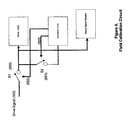
- the Controller (111) uses Switch Controls (502, 503) to control the switches S1 (500) and S2 (501).
- Switch S1 (500) When Switch S1 (500) is opened, the Drive Signal (100) is disconnected. At the same time, the switch S2 (501) can be closed. This allows the Controller (111) to place a train of pulses into the Driver (103) in order to calibrate the timing of the Output Signal Sampler and to calibrate the Extinction Ratio.
- this invention relies on correlating the photodiode sensor signal with the pattern of information transmitted over the optical communications link.
- the controller By capturing and storing the data pattern information and the corresponding sensor signal, the controller (111) can compute the correlation algorithms. Many algorithms that can accommodate multiple system responses are possible.
- One example of the correlation is as follows.
- the Digital Controller (111) can allow the charge stored in the capacitor C H (316) to decay to zero volts prior to sampling the Laser power output response.
- the response of the Signal Sampler in Figure 3 will be governed by the following equations:
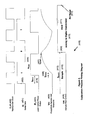
- Figure 6 shows the power measurement calibration. The following definitions apply:
- the laser will emit a pulse with a different level of power magnitude.
- V peak ⁇ 1 V m ⁇ 1 ⁇ 1 - e - Tl / R ⁇ 1 ⁇ C ⁇ 1
- V peak ⁇ 2 V m ⁇ 2 ⁇ 1 - e - T ⁇ 1 / R ⁇ 1 ⁇ C ⁇ 1
- T1 for a given value of period for a logic one transmission, in this case a constant.
- R1 and C1 correspondingly have substituted R, C since for a given circuit, the parameters are constant.
- equations 5 and 6 show how once the period and the circuit RC parameters are fixed, the quantity (1-e -T1/R1C1 ) becomes a constant and the peak values of the exponential rise are dependent only on the asymptotic values of the photodiode response.
- the asymptotic values bear a linear relationship to the laser output power.
- additional calibration processes need to be considered, which will control second order effects of the laser and photodiode transfer function such as temperature effects. It is then concluded that the Vpeak (407) of the exponential rise and decay of the photodiode sensing circuits will vary linearly would respect to the maximum amplitude Pmax (404) of the Laser Optical Power Output (403).
- the amplitude of the sensor signal is first maximized.
- sequence Signal Sampler delays 312 to 313. The delay that produces the strongest signal is chosen.
- the above calibration process can be modified for some applications if the process yield characteristics of the laser are understood. In that case, the sensor can still be calibrated but the process does not rely on the Optical Power Meter to determine how much power the laser puts out for all 1's and all 0's. Instead, process parameters can be used to coarsely determine the output power for a given setting of the Modulation Current Generator (103). During normal operation, a linear interpolation of the values of the sensor between the all 0's value and the all 1's value will determine the measured laser power output. These measured values of power output are then utilized to optimize performance on a continuous manner while the system is operational.
- the methods are related to ensuring the optimal value of extinction Ratio and minimal Bit Error Rate.
- the firmware imbedded in the Digital Controller (111) utilizes the results from the A/D conversion of the sensor and proceeds to make adjustments to the amplitude of the peak laser power in response to the logic high sent.
- the laser power for logic high needs to send a signal with a sufficiently large value according to the transmission protocol. With the precision power measurement circuit of this invention, the laser is not overdriven thus extending operating life.
- the Digital controller (111) makes adjustments to the minimal optical power in response to the logic low sent and.
- the minimal optical power is determined by the Bias Current Generator (102) and is adjusted above the threshold of the laser.
- the current needs to strike a balance between having too low of a value (needed to maximize extinction ratio) or too high of a value (needed to obtain a margin over the lasing threshold and to not operate over the noisy region of the laser near the threshold). Since the above adjustments are performed in a continuous manner, the laser is always operated at the optimal levels of power output.
Landscapes
- Physics & Mathematics (AREA)
- Electromagnetism (AREA)
- Engineering & Computer Science (AREA)
- Computer Networks & Wireless Communication (AREA)
- Signal Processing (AREA)
- Optics & Photonics (AREA)
- Condensed Matter Physics & Semiconductors (AREA)
- General Physics & Mathematics (AREA)
- Semiconductor Lasers (AREA)
- Optical Communication System (AREA)
- Investigating Or Analysing Materials By Optical Means (AREA)
Abstract
Description
- The present invention relates to a circuit and method used to calibrate and compensate for laser performance in systems such as an optical communications links, medical diagnostic systems and any other system utilizing lasers. Performance compensation is achieved in a non-invasive manner without disruption of the laser signal transmission or other operating parameters of the laser.
- Market trends demand increased levels of reliability and intelligence in laser systems. Particularly, in laser signal transmission there is the need to send information with reliable optical power signals. Reliability requires the transmitted signals to maintain a given signal strength as well as other performance parameters. Lasers undergo degradation due to aging, temperature changes, and other effects. This degradation causes the signal strength to be reduced resulting in a decrease of signal- to- noise ratio, extinction ratio and an increased Bit Error Rate.
- Prior art has utilized either analog controllers or mixed analog/digital controllers as opposed to the Digital Controller (111) shown in
Figure 1 below in the detailed description. - In order to properly control the laser Module (106), the Digital Controller (111) requires feedback information from light output (107). When the control system is operational, obtaining feedback information becomes problematic since the light output (107) constantly changes depending on the Drive Signal (100) the system is transmitting. Thus any attempts to measure the light output (107) will encounter errors, which can render the feedback information unusable.
- To perform a measurement of the light output (107), the Drive Signal (100) needs to be maintained at a fixed power level in order for the system to produce a steady value of the Light Output (107) so that calibration adjustments can be made. This procedure disrupts the signal transmission and, because of this, the transmitter cannot send information over the optical communications channel while the calibration is carried out. Disruption in communication is contrary to the goals of high reliability and 100% up time in present systems.
- If the Photodiode Sensor (109) is slow relative to the Laser Module (106), once the system is transmitting information, the Photodiode Sensor (109) cannot be effectively utilized to calibrate the amplitude of the Light Output (107) because the sensor may have a slower response than the laser. The Photodiode Sensor (109) operates as a band-limiting filter converting the response to a variety of waveforms as follows:
- An exponential rise and decay of the Photodiode Sensor (109) output is produced for a serial stream of the Drive Signal (100) comprised of all ones. For this data sequence, the average of the Photodiode Sensor (109) will exhibit the highest value;
- A Photodiode Sensor (109) output with an average value close to zero volts will be obtained for a serial stream of the Drive Signal (100) comprised of all zeros;
- The output of the Photodiode Sensor (109) will exhibit an average voltage value, which will between the maximum and minimum values described above depending on a generic sequence of date with mixed values of ones and zeros.
- To carry out a power measurement of the light output (107), the prior art has utilized a variety of methods. In one method the process has been as follows.
- • The digital input Drive Signal (100) is disconnected and a peak value of analog current from the Modulation Current Generator (103) is applied to the laser;
- • The Light Output (107) is measured with an optical power meter.
- • The Photodiode Sensor (109) generates a corresponding signal proportional to the light output;
- • Adjustments are made in the Controller (HI) in order to increase the magnitude of the optical power coming out of the laser to the desired level;
- • The adjustments in the Controller (111) affect the Bias Current Generator (102) and Modulation Current Generator (103), which in turn affect the Light Output (107) of the Laser Module (106);
- This approach has the disadvantage of requiring disconnection of the laser control system (114). Disconnection in many systems, such as communications equipment, is not acceptable.
- The process for another possible solution previously used is as follows:
- Produce a circuit to synthesize a high frequency calibration signal;
- Inject the calibration signal into the node between the Modulation Current Generator (103) and the laser module (106);
- Sense the calibration signal with the Photodiode Sensor (109);
- Add a special filter circuit between the photodiode sensor (109) and the Digital Controller (111);
- Detect the magnitude of the calibration signal with the Digital Controller (111).
- Because of errors in power measurement, transmission systems in prior art generally overdrive the laser to account for variations of temperature, aging and other effects. This approach significantly reduces the life of the laser.
-
US 6,414,974 B1 ,US 4,995,105 A ,US 5,502 ,298 A ,US 5,844,928 A ,US 2001/0024459 A1 ,US 6,282,218 B1 andUS 6,370,175 B1 describe prior art systems pertaining to the technological background of the present invention. - The present invention, as defined in
claims 1 and 13, provides a circuit and a method for calibrating the Light Output (107) of the laser without affecting the data transmission. This is consistent with goals of high reliability because at no time is the data transmission disrupted. - The present system contains a laser output measurement circuit used in a laser control system (114). The circuits contain a photodiode sensor (200), sample and hold amplifier (202), IC with synchronizer and delay circuits (206), and an analog to digital converter (204). The circuits measure the laser light output (107) while the laser Module (106) transmits signals. The measurement circuit tracks and stores the laser light output (107) signal using a Photodiode Sensor (109) and with a Sample/hold (202). The methods calculate the value of the laser light output (107) from mathematical relationships, which correlate the light output (107) of the laser Module (106) to the current value of the drive signal (100). Some of the distinguishing features in the present invention are 1) feedback information from the photodiode is obtained in a synchronous manner as a snapshot of the laser performance, and 2) the measurements are precise and calibrated, and 3) no disruption of the signal transmission occurs.
- An advantage of this invention is that laser power amplitude can be calibrated without interrupting the flow of information transmission.
- Another advantage of this invention is that the system can utilize multiple types of output responses from the Photodiode Sensor with the utilization of the appropriate correlation algorithm.
- Another advantage of this invention is that the transmitter optical power can be continuously maintained at the optimal value to achieve the target Extinction Ratio, Bit Error Rate and analog signal level.
- Another advantage of this invention is that the laser can be compensated for degradation due to aging.
Yet another advantage of this invention is that adjustments to account for temperature changes, aging and other effects are done only as needed and by the amount needed. This contributes to extending the life of the laser. - Details of the invention, and of the preferred embodiment thereof, will be further understood upon reference to the drawings, wherein closely related elements have the same number but different alphabetical suffixes, and further wherein:
-
Fig 1 illustrates a control system diagram for a laser transmitter. This control system shows a configuration presented in previous applications of the same inventor. -
Fig 2 illustrates a diagram of the Output Signal Sampler. -
Fig 3 illustrates an embodiment of the Output Signal Sampler. -
Fig 4 illustrates the timing diagram for the calibration process. -
Fig 5 illustrates a circuit, which can be used to facilitate field calibration. -
Fig 6 illustrates the power measurement calibration. -
Fig 7 illustrates the factory calibration of the sensor circuit. - The above-mentioned difficulties and problems of the prior art are overcome by the present invention.
- Referring to
FIG 1 , a block diagram is shown for a Laser Control System (114). The system consists of a drive Signal Input (100) applied to a Laser Module Driver (101), which contains a Bias Current Generator (102) and a Modulation Current Generator (103). A Bias Control Signal (112) and a Modulation Control Signal (113) control the current generators. The Driver (101) produces Modulation Current (104) and Bias Current (105) that are applied to the Laser Module (106). The Laser Module (106) in turn produces Light Output (107). The magnitude of the Light Output (107) bears a relationship to the magnitude of the Modulation Current (104) and the Bias Current (105). A portion of the Light Output (107) from the laser is sensed. This portion constitutes the Optical Power Sense (108), which is coupled to a Photodiode Sensor (109). The Photodiode Sensor Output (110) is connected to a Digital Controller (111). The Digital Controller (111) contains algorithms for laser control and also determines the magnitudes of the Bias Current Generator (102) and Modulation Current (103). -
Figure 2 shows the output signal sampler apparatus of this invention. This consists of a Photodiode Sensor (109), which generates a Photodiode Signal (201) in response to the application of a portion of the Laser Light Output (107). The Photodiode Output may be a fast response or an exponential rise and decay signal. The Sample and Hold Amplifier (202) receives the Photodiode Sensor Signal (201) and stores the value of the signal at the appropriate time as directed by the Sample and Hold Control (205). Once the Sample and Hold Amplifier (202) has stored the signal, it is sent to the Analog to Digital Converter (204), which is contained in the Digital Controller (111). The Sample and Hold Amplifier (202) is connected to the Analog to Digital Converter (204). - The Sample and Hold Control (205) is produced by the Synchronizer and Delay Circuits (206). These circuits utilize real-time information of the state of the Drive Signal (100), which connects to the Drive Signal (100) at (208) in order to determine when the Sample and Hold Control (205) is activated. The Synchronizer and Delay Circuits (206) are controlled by the Digital Controller (111) with the necessary Logic Output (207). The Digital Controller (111) contains algorithms that are capable of utilizing a multiplicity of Photodiode Sensor information including an exponential rise and decay, a square wave response, and an average signal output. The algorithms utilize information related to the sequence of values of the Drive Signal (100) input and correlate those values to the magnitude of the Photodiode Sensor (109) output. In addition, the controller can then make adjustments to the Bias Current (105) and Modulation Current (104), in order to optimize the extinction ratio and the Bit Error Rate.
-
Figure 3 is an embodiment of the Output Signal Sampler in this invention. The Drive Signal (100) applied to the Driver (103) produces a Light Output (107). A portion of the optical power is coupled to the Photodiode Sensor (109). The Photodiode Sensor (109) produces a current, which is converted to a voltage by the Transimpedance Amplifier (301). This voltage drives the Sample and Hold Amplifier (302), which in turn produces a steady sample of the sensor signal at (304) to the Analog to Digital Converter (304). The Sample and Hold Amplifier (202) stores the sensor information in a Capacitor CH (316). The capacitor is chosen so that the capturing of the sensor signal is done at high speed while at the same time the capacitor maintains the value of the captured sensor signal during the analog to digital conversion. In general, for optical telecommunications, the capacitor may need to be relatively small in the tens of picofarads in order for the Sample and Hold Amplifier (202) to successfully track the sensor signal. The Transimpedance Amplifier (301) and the Sample and Hold Amplifier (202) are designed in such a way that they will be substantially faster then the Photodiode Sensor (109) in order to insure that the Photodiode Sensor (109) determines the frequency response. A critical feature of the present invention is the appropriate timing of the Sample and Hold Control (205). This control must be able to capture the Photodiode Sensor (109) signal at a predictable time in order to anticipate the state of the Drive Signal (100) and the Light Output (107). The timing synchronization circuit determines this. This circuit starts by sampling the Drive Signal (100) at (315). This is done with the use of a Buffer (314) in order to avoid a significant load on the Drive Signal (100). The output of the Buffer (314) is sent to a set of n signal propagation delays. These delays consist of Delay 1 (312) to Delay n (313). These delays connect to Digital Multiplexer (309) through Inputs (310) to (311). The Digital Controller utilizes the Input Select (308) of the Digital Multiplexer (309) in order to select any of the n signal propagation delays. A zero to one transmission of the Drive Signal (100) will cause, after a time delay, a zero to one transition at the Set Input (307) of the Set Reset Latch (305). This transition in turn causes a zero to one transition of the Sample and Hold Control (205), which places the Sample and Hold Amplifier (202) in hold mode in order to prepare the system for an analog to digital conversion. After the analog to digital conversion is completed the Set Reset Latch (305), is placed in reset mode by the Reset Signal (306) generated by the Digital Controller (111). This last step will then place the Sample and Hold Amplifier (202) in sample mode so that the system can be ready for the next calibration cycle. -
Figure 3 shows the propagation delays associated with the Output Signal Sampler. The following definitions apply: - t1= Buffer (314) input to output propagation delay
- t2= Selected propagation delay.
- t3 Digital Multiplexer (309) propagation delay.
- t4 Set input to Output propagation delay for Set Reset Latch (305).
- t5= Propagation delay from Sample and Hold Control S/H (408) input to the opening of the internal switch in the Sample and Hold Amplifier (202).
- tDrive (414)= Propagation delay across the Driver (103) + time for the Laser (106) to switch logic state
- tSense (406) = Time for the Photodiode Sensor (109) to respond + time for the Transimpedance Amplifier (301) to respond
- tCapture (414) = Time for the Sample and Hold Amplifier (202) to track the photodiode sensor signal.
- In order to maximize Vpeak (407), the following equation must be satisfied:

When the S/H (408) is in hold mode after the transition at 409, the Analog to Digital Converter (204) performs an analog to digital conversion, which will last for a period of time tA/D (412). The duration of the analog to digital conversion can be relatively slow as required by the Analog to Digital Converter (204). At the end of the conversion, the Digital Controller (111) will cause the S/H (408) signal to experience a Reset (412) transition to the sample mode with the use of the Reset Control (306). The embodiment shown inFigure 3 may utilize MOS technology components for a given data rate of transmission. Synchronization of the timing characteristics and delays as indicated byEquation 2 can be best achieved by including the Signal Sampler circuits ofFigure 3 in the same integrated circuit as the Driver (103). If a single integrated circuit is not available, then the Signal Sampler circuits must be implemented with the appropriate technology in order to match the speed requirements of the propagation delays associated with the laser Driver (103). Very fast Silicon Germanium and other technologies are available. In some applications, fine-tuning and modifications of the embodiment ofFigure 3 will be necessary to keep up with fast transmission rates. In these cases the same principles of the invention will apply and the task will consist of selecting the appropriate configuration of high-speed components. -
Figure 4 shows the timing of the in line calibration of the laser optical power. As a reference to the timing of the system consider the system clock that is utilized by the transponder. This is the clock CLK (400). The clock (400) is utilized in the system to generate Serial Data Di (401). In this example the Serial Data Di (401) consists of thesequence 101. The data transmission of the timing diagram in the illustration corresponds to NRZ-L. After the zero to one transition of the Serial Data Di at (402), the data flows through the Driver (103) and causes a zero to one transition in Laser Optical Power PL (403). This transition of the Laser Optical Power (403) happens after a delay tDrive (413), corresponding to the delay of the signal flowing through the Driver (103) and the Laser (106). A given setting of the Bias Current Generator (102) places the Laser (106) slightly above the threshold. This setting can be adjusted and controller independently from the signal modulation current. For the purpose of calibrating the Light Output (107) focus on the control of the Modulation Current Generator (103). For the pulse of the Serial Data Di (401), there is a corresponding amplitude of the Laser Optical Power Output PL (403). The magnitude of the optical power is noted as Pmax (404). The laser optical power corresponding to the transmission of a logical 1 will vary depending on the setting of the Modulation Current Generator (103), the Laser (106) characteristics and the effects of factors such as temperature and aging on the Laser (106). The Photodiode Sample Hold Response VPS (405) will start sensing the Laser (106) output after a delay of tsense (406). The Sample and Hold Amplifier (202) will start increasing its voltage in an exponential manner reaching a maximum value Vpeak (407). High frequency models have been determined that demonstrate how the combination of amplifiers and Photodiode Sensor (109) can respond with an exponential rise and decay characteristic. Associated circuit components such as resistors and capacitors can be utilized to ensure there is a dominant pole response resulting in a controlled exponential characteristic without signal ringing. There can be high performance circuit implementations of the laser sensor circuits where the Photodiode sensor (109), Transimpedance Amplifier (301) and Sample and Hold Amplifier (202) exhibit a response with a bandwidth fast enough to keep up with the laser bandwidth. In this case, a rather fast rise and fall signal will result rather than the exponential rise and decay. The exponential rise and decay characteristic is illustrated here because it is fairly common for laser packages to be available with an integrated low-cost monitoring photodiode. These integrated packages normally have a monitoring photodiode that exhibits a slow frequency response.
After a delay of tSynch (415) from the zero to one transition of the Serial Data Di (401), the Sample and Hold Control S/H (408) will experience a transition from Sample (410) mode to Hold (411) mode at 409. Transition at this point in time ensures that it is possible to capture the maximum possible value of Vpeak (407). This will produce a higher resolution in our measurement system. - Signal strength optimization of the Laser power sensor.
The Digital Controller (111), upon power up goes through an initialization process. Part of the initialization routine consists of a process used to optimize the sensor signal. The objective of the process is to maximize the value of Vpeak (407). Maximizing the value of Vpeak increases the resolution and accuracy of the laser power measurement system.
This is accomplished with an iterative process where the Digital Controller (111) will automatically select the timing delays one at a time and determine which produces the highest value of the Vpeak (407). This process can be carried out during the factory test of the transmitter. The needed value of the timing delay is then stored in the internal memory of the Digital Controller (111) so it can be used in the field. The process can also be carried out in the field with an addition to the circuit ofFigure 3 . - This is illustrated in
Figure 5 . The Controller (111) uses Switch Controls (502, 503) to control the switches S1 (500) and S2 (501). When Switch S1 (500) is opened, the Drive Signal (100) is disconnected. At the same time, the switch S2 (501) can be closed. This allows the Controller (111) to place a train of pulses into the Driver (103) in order to calibrate the timing of the Output Signal Sampler and to calibrate the Extinction Ratio. - To carry out continuous laser performance compensation, this invention relies on correlating the photodiode sensor signal with the pattern of information transmitted over the optical communications link. By capturing and storing the data pattern information and the corresponding sensor signal, the controller (111) can compute the correlation algorithms. Many algorithms that can accommodate multiple system responses are possible. One example of the correlation is as follows.
- Consider the exponential rise and decay of the Photodiode Sample Hold Response (405). The Digital Controller (111) can allow the charge stored in the capacitor CH (316) to decay to zero volts prior to sampling the Laser power output response. The response of the Signal Sampler in
Figure 3 will be governed by the following equations: - Exponential rise

Where Vm represents the asymptotic maximum value of the exponential rise response, R and C are the equivalent circuit constants and V(t) is the voltage at the Sample and Hold Amplifier (202). - Exponential decay

Where VP represents the maximum value attained during the exponential rise response as determined by the circuit parameters and the data rate of transmission, R and C are the equivalent circuit constants and V(t) is the voltage at the Sample and Hold Amplifier (202). -
Figure 6 shows the power measurement calibration. The following definitions apply: - PPH1 (600)= Laser power pulse received at the photodiode for a given setting of laser power output. This is proportional to the pulse of power that the laser emits in response to the logic one transmission.
- PPHMax1 (604)= Maximum value of Laser power pulse received at the photodiode. The magnitude of the photodiode power is determined by the Driver (103), Laser (106) and the amount of light coupled from the laser to the photodiode.
- V1(t)(601)= Time dependent response of the photodiode(109) output, the Transimpedance Amplifier (301) and the Sample and Hold Amplifier (202). This response is the corresponding response to PPH1 (600).
- Vm1 (606)= Asymptotic value of the exponential response for V1 (t) (601). This is proportional to PPHMax1(604). The proportionality constant is the Responsivity of the photodiode.
- Vpeak1 (605)= Peak value of exponential response corresponding to the end of the pulse for the transmission of a logic one.
- Similarly, for a different set of conditions, the laser will emit a pulse with a different level of power magnitude. The following definitions apply:
- PPH2(602)= Laser power pulse received at the photodiode for a second setting of laser power output.
- PPHMax2 (607)= Maximum value of Laser power pulse received at the photodiode.
- V2(t) (603)= Time dependent response of the photodiode(109) output, the Transimpedance Amplifier (301) and the Sample and Hold Amplifier (202). This response is the corresponding response to PPH2 (602).
- Vm2 (609)= Asymptotic value of the exponential response for V2(t) (603). This is proportional to PPHMax2 (607). The proportionality constant is the Responsivity of the photodiode.
- Vpeak2 (608)= Peak value of exponential response corresponding to the end of the pulse for the transmission of a logic one.
- Focusing now on the corresponding equations the following relationships are obtained:


Where t has been substituted by T1 for a given value of period for a logic one transmission, in this case a constant. R1 and C1 correspondingly have substituted R, C since for a given circuit, the parameters are constant.
In general, equations 5 and 6 show how once the period and the circuit RC parameters are fixed, the quantity (1-e -T1/R1C1) becomes a constant and the peak values of the exponential rise are dependent only on the asymptotic values of the photodiode response. The asymptotic values bear a linear relationship to the laser output power.
In this case additional calibration processes need to be considered, which will control second order effects of the laser and photodiode transfer function such as temperature effects.
It is then concluded that the Vpeak (407) of the exponential rise and decay of the photodiode sensing circuits will vary linearly would respect to the maximum amplitude Pmax (404) of the Laser Optical Power Output (403). - The amplitude of the sensor signal is first maximized. At 700 apply a continuous stream of all 1's to the data input. At 701, while maintaining the stream of all 1's, sequence Signal Sampler delays 312 to 313. The delay that produces the strongest signal is chosen. At 702, apply a continuous stream of all 0's. At 703, measure the value of the laser power with an optical power meter. Also an A/D conversion to measure the baseline sensor signal for a zero transmission is performed. At 704, then apply a stream of all 1's. At 705, while measuring power with optical power meter, continuously adjust magnitude of laser power by controlling the Modulation Current Generator (103) until the maximum possible value of the laser power output is reached. The corresponding sensor output is measured and stored in the Digital Controller (111).
- The above calibration process can be modified for some applications if the process yield characteristics of the laser are understood. In that case, the sensor can still be calibrated but the process does not rely on the Optical Power Meter to determine how much power the laser puts out for all 1's and all 0's. Instead, process parameters can be used to coarsely determine the output power for a given setting of the Modulation Current Generator (103).
During normal operation, a linear interpolation of the values of the sensor between the all 0's value and the all 1's value will determine the measured laser power output. These measured values of power output are then utilized to optimize performance on a continuous manner while the system is operational. - The methods are related to ensuring the optimal value of extinction Ratio and minimal Bit Error Rate. The firmware imbedded in the Digital Controller (111) utilizes the results from the A/D conversion of the sensor and proceeds to make adjustments to the amplitude of the peak laser power in response to the logic high sent. The laser power for logic high needs to send a signal with a sufficiently large value according to the transmission protocol. With the precision power measurement circuit of this invention, the laser is not overdriven thus extending operating life. The Digital controller (111) makes adjustments to the minimal optical power in response to the logic low sent and. The minimal optical power is determined by the Bias Current Generator (102) and is adjusted above the threshold of the laser. The current needs to strike a balance between having too low of a value (needed to maximize extinction ratio) or too high of a value (needed to obtain a margin over the lasing threshold and to not operate over the noisy region of the laser near the threshold). Since the above adjustments are performed in a continuous manner, the laser is always operated at the optimal levels of power output.
-
- 1. A circuit that precisely calibrates the laser optical power in a continuous manner without disrupting the flow of information in the optical communications link.
- 2. A method that utilizes knowledge of the measured value of the laser optical power and makes necessary adjustments to optimize the values of the Extinction Ratio and Bit Error Rate.
- 3. A circuit that can utilize any type of response from the sensing photodiode.
- 4. A method that utilizes knowledge of the information sent to the optical communications link to determine how the laser should be performing.
- 5. A circuit and method utilized to compensate for aging, temperature rise and other degradation effects of the laser without interrupting the flow of information transmitted.
- 6. A circuit and method that compensates for aging, temperature rise and other degradation effects of a laser only as needed at any point in time rather than at the beginning when power is turned on or at the factory.
- 7. A process that automatically maximizes the magnitude of the photodiode power sensor signal for a laser.
- 8. A circuit to capture a sense the laser output where the sensing is coordinated with the transmission signal.
- 9. A circuit as in 8, where the associated timing of the circuit is automatically optimized.
- Consequently, while the foregoing description has described the principle and operation of the present invention in accordance with the provisions of the patent statutes, it should be understood that the invention may be practiced otherwise as illustrated and described above and that various changes in the size, shape, and materials, as well as on the details of the illustrated method of operation may be made, within the scope of the appended claims without departing from the spirit and scope of the invention.
Claims (18)
- An apparatus containing an output signal sampler (210) used in a laser control system (114), the output signal sampler comprising:a photodiode sensor (109) for generating a photodiode signal (201) in response to the application of a portion of a laser light output signal (107) whereby the laser light output signal may be a fast response, or an exponential rise and decay signal;a sample and hold amplifier (202) for receiving the photodiode signal (201) and storing a value of the photodiode signal (201) at an appropriate time as directed by a sample and hold control (205);an analog to digital converter (204) for receiving the value of the photodiode signal (201) from the sample and hold amplifier (202);an integrated circuit with a synchronizer and delay circuit (206) for producing the sample and hold control (205) whereby the synchronizer and delay circuit (206) utilize real time information of the state of a laser drive signal (100); anda digital controller (111) for controlling the synchronizer and delay circuit (206) with a logic output (207) wherein the digital controller (111) contains said converter (204) and a plurality of algorithms and wherein the digital controller (111) is adapted to optimize an extinction ratio and a bit error rate by adjusting a bias current (105) and a modulation current (104).
- The apparatus of claim 1, wherein the sample and hold amplifier (202) comprises a capacitor (316) for storing the samples of the photodiode signal (201).
- The apparatus of claim 2, wherein the digital controller (111) comprises the analog to digital converter (204) for converting analog samples of the photodiode signals (201) into digital samples.
- The apparatus of claim 2 or 3, wherein the capacitor (316) is adapted to store the samples of the photodiode signal (201) at a speed sufficient to ensure that the photodiode sensor determines the frequency response while the capacitor concurrently maintains the value of the stored sample during the analog to digital conversion
- The apparatus of any of claims 2 to 4, wherein the output signal sampler (210) comprises said synchronizer and delay circuit (206) for controlling the sample and hold amplifier (202) using real-time information on the laser drive signal (100) to provide appropriate timing to said sample and hold control (205).
- The apparatus of claim 5, wherein the synchronizer and delay circuit (206) is adapted to sample the photodiode signal (201) at a predictable time in order to anticipate the state of the laser input signal (100) and the laser light output signal (107).
- The apparatus of any of claims 2 to 6, wherein the digital controller (111) is adapted to apply an algorithm using exponential rise and decay information on the photodiode signals (201) to perform the correlation.
- The apparatus of any of claims 2 to 6, wherein the digital controller (111) is adapted to apply an algorithm using square wave response information on the photodiode signals (201) to perform the correlation.
- The apparatus of any of claims 2 to 6, wherein the digital controller (111) is adapted to apply an algorithm using average signal output information on the photodiode signals (201) to perform the correlation.
- The apparatus of any of claims 2 to 9, wherein the digital controller (111) is adapted to apply an algorithm using a sequence of values of the laser drive signal (100) to perform the correlation.
- The apparatus of any of claims 2 to 10, wherein the sample and hold amplifier (202) is faster than the photodiode sensor (109).
- A method of operating an apparatus according to claim 1, the method comprising:measuring the laser light output signal (107);producing and storing samples of the measured laser light output signal (107);correlating the samples of the laser light output signal to real time information on the laser drive signal (100); andcontrolling a laser by causing adjustments to the modulation and bias currents applied to the laser.
- The method of claim 12, wherein the samples of the laser light output signal are stored in a capacitor (316).
- The method of claim 13, wherein the capacitor (316) is adapted to store the samples at a speed sufficient to ensure that the photodiode sensor determines the frequency response while the capacitor concurrently maintains the value of the stored sample during an analog to digital conversion.
- The method of any of claims 12 to 14, wherein the step of producing and storing samples of the measured laser output signal (107) is performed using a photodiode sensor (109) and a sample and hold amplifier (202).
- The method of claim 15, wherein the sample and hold amplifier (202) is faster than the photodiode sensor (109).
- The method of any of claims 12 to 16, further comprising using a time synchronization circuit (206) to sample the measured laser light output signal (107) at a predictable time in order to anticipate the state of the laser drive signal (100) and the laser light output signal (107).
- The method of any of claims 12 to 17 wherein the step of producing and storing samples of the measured laser light output signal (107) further comprises:buffering the laser drive signal (100);delaying the buffered laser drive signal to produce a set of delayed laser drive signals;selecting a particular delayed laser drive signal from the set of delayed laser drive signals;capturing the selected particular laser drive signal in a sample and hold amplifier (202) to produce a delayed laser drive signal sample;placing the sample and hold amplifier (202) in a hold mode during an analog to digital conversion of the delayed laser drive signal sample;converting the delayed laser drive signal sample to a digital signal sample; andresetting the sample and hold amplifier (202) for a next sample capturing cycle.
Applications Claiming Priority (1)
| Application Number | Priority Date | Filing Date | Title |
|---|---|---|---|
| PCT/US2003/000463 WO2004064210A1 (en) | 2003-01-08 | 2003-01-08 | Apparatus and method for measurement of dynamic laser signals |
Publications (3)
| Publication Number | Publication Date |
|---|---|
| EP1529327A1 EP1529327A1 (en) | 2005-05-11 |
| EP1529327A4 EP1529327A4 (en) | 2005-08-31 |
| EP1529327B1 true EP1529327B1 (en) | 2009-03-04 |
Family
ID=32710270
Family Applications (1)
| Application Number | Title | Priority Date | Filing Date |
|---|---|---|---|
| EP03701250A Expired - Lifetime EP1529327B1 (en) | 2003-01-08 | 2003-01-08 | Apparatus and method for measurement of dynamic laser signals |
Country Status (7)
| Country | Link |
|---|---|
| US (4) | US7505498B2 (en) |
| EP (1) | EP1529327B1 (en) |
| AT (1) | ATE424640T1 (en) |
| AU (1) | AU2003202238A1 (en) |
| CA (1) | CA2475850A1 (en) |
| DE (1) | DE60326457D1 (en) |
| WO (1) | WO2004064210A1 (en) |
Families Citing this family (66)
| Publication number | Priority date | Publication date | Assignee | Title |
|---|---|---|---|---|
| JP4312573B2 (en) * | 2003-10-27 | 2009-08-12 | 株式会社リコー | Semiconductor laser drive circuit |
| JP4754170B2 (en) * | 2003-12-03 | 2011-08-24 | パナソニック株式会社 | Laser drive circuit and optical communication device |
| US7333521B1 (en) * | 2003-12-04 | 2008-02-19 | National Semiconductor Corporation | Method of sensing VCSEL light output power by monitoring electrical characteristics of the VCSEL |
| US20050191059A1 (en) * | 2004-01-12 | 2005-09-01 | Clariphy | Use of low-speed components in high-speed optical fiber transceivers |
| TWI290640B (en) * | 2004-06-16 | 2007-12-01 | Mediatek Inc | Laser power controller and method for performing an auto power control |
| US7447438B2 (en) * | 2004-07-02 | 2008-11-04 | Finisar Corporation | Calibration of digital diagnostics information in an optical transceiver prior to reporting to host |
| US8639122B2 (en) * | 2004-07-02 | 2014-01-28 | Finisar Corporation | Filtering digital diagnostics information in an optical transceiver prior to reporting to host |
| US7693491B2 (en) * | 2004-11-30 | 2010-04-06 | Broadcom Corporation | Method and system for transmitter output power compensation |
| US7634197B2 (en) * | 2005-01-12 | 2009-12-15 | Finisar Corporation | Compensation for temperature and voltage effects when monitoring parameters in a transceiver module |
| US7369591B1 (en) * | 2005-01-14 | 2008-05-06 | National Semiconductor Corporation | System for controlling peaking for a driver for a vertical-cavity surface-emitting laser |
| US7630422B1 (en) | 2005-01-14 | 2009-12-08 | National Semiconductor Corporation | Driver for vertical-cavity surface-emitting laser and method |
| US8036539B2 (en) * | 2005-06-28 | 2011-10-11 | Finisar Corporation | Gigabit ethernet longwave optical transceiver module having amplified bias current |
| GB2432037B (en) * | 2005-11-01 | 2011-04-20 | Agilent Technologies Inc | A method and system for stabilizing operation of laser sources |
| US20080138080A1 (en) * | 2006-12-08 | 2008-06-12 | Alcatel Lucent | Controller detection |
| EP2031744A1 (en) * | 2007-08-31 | 2009-03-04 | Bombardier Transportation GmbH | Power converter, in particular for railway traction vehicle |
| JP2009200242A (en) * | 2008-02-21 | 2009-09-03 | Fujitsu Ltd | Optical transmitter, and control method |
| US8447570B2 (en) * | 2008-05-21 | 2013-05-21 | Infineon Technologies Ag | Predictive sensor readout |
| US9300405B2 (en) * | 2011-12-02 | 2016-03-29 | Semtech Corporation | Closed loop optical modulation amplitude control |
| US9450696B2 (en) * | 2012-05-23 | 2016-09-20 | Vadum, Inc. | Photonic compressive sensing receiver |
| JP5999179B2 (en) * | 2012-06-07 | 2016-09-28 | 富士通株式会社 | Photodetector, photodetection method, and optical transmitter |
| US8923353B2 (en) * | 2012-10-26 | 2014-12-30 | Broadcom Corporation | Laser driver modulation and bias control scheme |
| US9881250B2 (en) * | 2013-06-07 | 2018-01-30 | Fisher Controls International Llc | Methods and apparatus for RFID communications in a process control system |
| WO2015006902A1 (en) * | 2013-07-15 | 2015-01-22 | 华为技术有限公司 | Wavelength alignment method and device, and optical network system |
| US9258056B2 (en) * | 2013-12-20 | 2016-02-09 | Juniper Networks, Inc. | Methods and apparatus for monitoring and controlling the performance of optical communication systems |
| US9432121B2 (en) * | 2014-06-05 | 2016-08-30 | Xilinx, Inc. | Optical communication circuits |
| US10303134B2 (en) | 2015-04-10 | 2019-05-28 | Fisher Controls International Llc | Methods and apparatus for multimode RFST communications in process control systems |
| US10177841B2 (en) * | 2016-03-31 | 2019-01-08 | Mellanox Technologies, Ltd. | Electro-optic transceiver module with wavelength compensation |
| US20170288369A1 (en) * | 2016-04-01 | 2017-10-05 | Macom Technology Solutions Holdings, Inc. | Dual closed loop for laser power control |
| GB2541291B (en) * | 2016-07-08 | 2018-06-20 | Hilight Semiconductor Ltd | Laser power controller |
| US9806807B1 (en) * | 2016-07-12 | 2017-10-31 | Adtran, Inc. | Automatic rogue ONU detection |
| US10263384B2 (en) * | 2016-10-14 | 2019-04-16 | Lumenis Ltd. | Laser system having a dual pulse-length regime |
| US10481246B2 (en) * | 2017-05-22 | 2019-11-19 | Analog Devices Global Unlimited Company | Photo-diode emulator circuit for transimpedance amplifier testing |
| US10938365B2 (en) | 2018-05-18 | 2021-03-02 | Macom Technology Solutions Holdings, Inc. | Variable step size to reduce convergence time of a control loop |
| US11848653B2 (en) | 2018-05-18 | 2023-12-19 | Macom Technology Solutions Holdings, Inc. | Method and apparatus to speed convergence and control behavior of digital control loop |
| US11067672B2 (en) | 2018-06-19 | 2021-07-20 | Waymo Llc | Shared sample and convert capacitor architecture |
| US11005573B2 (en) | 2018-11-20 | 2021-05-11 | Macom Technology Solutions Holdings, Inc. | Optic signal receiver with dynamic control |
| EP3683906A1 (en) * | 2019-01-15 | 2020-07-22 | ams AG | Temperature sensor, laser circuit, light detection and ranging system and method |
| EP4032238A4 (en) | 2019-09-19 | 2023-09-20 | MACOM Technology Solutions Holdings, Inc. | USING ISI OR Q CALCULATION TO ADJUST EQUALIZER SETTINGS |
| FR3101218B1 (en) | 2019-09-23 | 2022-07-01 | Macom Tech Solutions Holdings Inc | EQUALIZER ADAPTATION BASED ON EYE MONITORING DEVICE MEASUREMENTS |
| WO2021076800A1 (en) | 2019-10-15 | 2021-04-22 | Macom Technology Solutions Holdings, Inc. | Finding the eye center with a low-power eye monitor using a 3-dimensional algorithm |
| CN110954771A (en) * | 2019-12-17 | 2020-04-03 | 武汉英飞光创科技有限公司 | Aging method for COC (chip on chip) of optical module |
| US11575437B2 (en) | 2020-01-10 | 2023-02-07 | Macom Technology Solutions Holdings, Inc. | Optimal equalization partitioning |
| TWI884203B (en) | 2020-01-10 | 2025-05-21 | 美商Macom技術方案控股公司 | Transceiver, method for receiving and processing an optical signal, and optical module |
| CA3111302A1 (en) * | 2020-03-09 | 2021-09-09 | Thorlabs Quantum Electronics, Inc. | Tunable laser assembly and method of control |
| US11689283B1 (en) * | 2020-03-30 | 2023-06-27 | Meta Platforms, Inc. | Free-space optical communication system using a backchannel for power optimization |
| US12265125B2 (en) | 2020-06-11 | 2025-04-01 | Tektronix, Inc. | System and method for separation and classification of signals using cyclic loop images |
| US12013423B2 (en) | 2020-09-30 | 2024-06-18 | Macom Technology Solutions Holdings, Inc. | TIA bandwidth testing system and method |
| US11658630B2 (en) | 2020-12-04 | 2023-05-23 | Macom Technology Solutions Holdings, Inc. | Single servo loop controlling an automatic gain control and current sourcing mechanism |
| US12328242B2 (en) * | 2021-02-03 | 2025-06-10 | Tektronix, Inc. | Eye classes separator with overlay, and composite, and dynamic eye-trigger for humans and machine learning |
| US11616529B2 (en) | 2021-02-12 | 2023-03-28 | Macom Technology Solutions Holdings, Inc. | Adaptive cable equalizer |
| US12442852B2 (en) | 2022-03-30 | 2025-10-14 | Tektronix, Inc. | Tuning a device under test using parallel pipeline machine learning assistance |
| US11923896B2 (en) * | 2021-03-24 | 2024-03-05 | Tektronix, Inc. | Optical transceiver tuning using machine learning |
| US20240235669A1 (en) * | 2021-03-24 | 2024-07-11 | Tektronix, Inc. | Systems and methods for tuning and measuring a device under test using machine learning |
| US11923895B2 (en) | 2021-03-24 | 2024-03-05 | Tektronix, Inc. | Optical transmitter tuning using machine learning and reference parameters |
| US11940889B2 (en) | 2021-08-12 | 2024-03-26 | Tektronix, Inc. | Combined TDECQ measurement and transmitter tuning using machine learning |
| US11907090B2 (en) | 2021-08-12 | 2024-02-20 | Tektronix, Inc. | Machine learning for taps to accelerate TDECQ and other measurements |
| US12146914B2 (en) | 2021-05-18 | 2024-11-19 | Tektronix, Inc. | Bit error ratio estimation using machine learning |
| US12571841B2 (en) | 2021-06-04 | 2026-03-10 | Tektronix, Inc. | General digital signal processing waveform machine learning control application |
| CN114037117B (en) * | 2021-10-08 | 2024-11-05 | 苏州热工研究院有限公司 | A predictive management method for photoelectric converters in nuclear power plants |
| US20230111084A1 (en) * | 2021-10-12 | 2023-04-13 | Zebra Technologies Corporation | Methods and devices for an electrically efficient green laser diode drive system with boost servo |
| US12416662B2 (en) | 2022-01-14 | 2025-09-16 | Tektronix, Inc. | Machine learning model training using de-noised data and model prediction with noise correction |
| CN114498293B (en) * | 2022-03-30 | 2022-07-19 | 成都明夷电子科技有限公司 | Optical module adjusting method with temperature compensation |
| US20240243547A1 (en) * | 2023-01-13 | 2024-07-18 | Streamlight, Inc. | Driver circuit and method for a semiconductor laser |
| US12199606B2 (en) | 2023-05-16 | 2025-01-14 | Macom Technology Solutions Holdings, Inc. | Level shifter with expanded voltage range |
| CN118091358A (en) * | 2024-04-28 | 2024-05-28 | 四川映塞科技有限责任公司 | A semiconductor testing system and working method thereof |
| CN120016255B (en) * | 2025-04-17 | 2025-06-20 | 深圳市三千米光电科技有限公司 | Modularized quick-dismantling detection interface infrared laser module |
Family Cites Families (115)
| Publication number | Priority date | Publication date | Assignee | Title |
|---|---|---|---|---|
| US3346811A (en) | 1964-02-24 | 1967-10-10 | Allis Chalmers Mfg Co | Means for sensing conditions in high potential region and for transmitting such intelligence by light means to low potential regions |
| US4000397A (en) | 1975-03-21 | 1976-12-28 | Spectra-Physics, Inc. | Signal processor method and apparatus |
| US4168398A (en) | 1976-11-10 | 1979-09-18 | Nippon Electric Co., Ltd. | Initial acquisition signal detection system for TDMA satellite communication |
| US4164036A (en) | 1977-12-07 | 1979-08-07 | Honeywell Inc. | Quadrature correlation phase reversal pulse detector |
| SE413808B (en) | 1978-09-22 | 1980-06-23 | Asea Ab | METDON FOR TRANSFER OF METSIGNALS THROUGH AN OPTICAL LINK |
| US4290297A (en) | 1979-05-14 | 1981-09-22 | Rousemount Inc. | Optically coupled calibrator for transmitters |
| DE3013533A1 (en) | 1980-04-08 | 1981-10-15 | Siemens Ag | CIRCUIT ARRANGEMENT WITH A LASER DIODE FOR TRANSMITTING MESSAGE SIGNALS VIA A LIGHT WAVE GUIDE |
| JPS6113946Y2 (en) | 1981-05-28 | 1986-04-30 | ||
| DE3137497A1 (en) | 1981-09-21 | 1983-04-07 | Siemens Ag | OPTICAL TRANSMISSION SYSTEM FOR HIGH FREQUENCY DIGITAL SIGNALS |
| JPS5964286U (en) | 1982-10-21 | 1984-04-27 | 株式会社サクラクレパス | marking pen |
| US4558465A (en) | 1983-09-19 | 1985-12-10 | Rca Corporation | Switched bias scheme for high speed laser transmitter |
| US4734873A (en) | 1984-02-02 | 1988-03-29 | Honeywell Inc. | Method of digital process variable transmitter calibration and a process variable transmitter system utilizing the same |
| US4677536A (en) | 1986-03-17 | 1987-06-30 | Tektronix, Inc. | AC Current sensing circuit |
| US4758779A (en) | 1986-04-07 | 1988-07-19 | Tektronix, Inc. | Probe body for an electrical measurement system |
| GB2192510A (en) | 1986-07-12 | 1988-01-13 | Stc Plc | Optical receiver |
| US4745361A (en) | 1987-03-03 | 1988-05-17 | University Of Rochester | Electro-optic measurement (network analysis) system |
| US4910458A (en) | 1987-03-24 | 1990-03-20 | Princeton Applied Research Corp. | Electro-optic sampling system with dedicated electro-optic crystal and removable sample carrier |
| US5272434A (en) | 1987-06-20 | 1993-12-21 | Schlumberger Technologies, Inc. | Method and apparatus for electro-optically testing circuits |
| DE8710852U1 (en) | 1987-08-07 | 1988-12-08 | Siemens AG, 1000 Berlin und 8000 München | Chip card |
| JP3175935B2 (en) | 1987-09-30 | 2001-06-11 | 株式会社東芝 | Optical fiber sensor |
| JPH01150879A (en) | 1987-12-08 | 1989-06-13 | Nissan Motor Co Ltd | Radio type production management information medium |
| US4796266A (en) | 1987-12-21 | 1989-01-03 | Bell Communications Research, Inc. | Laser driver circuit with dynamic bias |
| US4939446A (en) | 1988-03-30 | 1990-07-03 | Rogers Wesley A | Voltage transmission link for testing EMI susceptibility of a device or circuits |
| DE3817836A1 (en) | 1988-05-26 | 1989-11-30 | Philips Patentverwaltung | OPTICAL TRANSMITTER WITH A LASER DIODE |
| DE3818168A1 (en) | 1988-05-26 | 1990-04-05 | Krone Ag | RECEIVER PRE-AMPLIFIER FOR AN OPTICAL MESSAGE RANGE |
| US4875006A (en) | 1988-09-01 | 1989-10-17 | Photon Dynamics, Inc. | Ultra-high-speed digital test system using electro-optic signal sampling |
| US4994675A (en) | 1989-04-28 | 1991-02-19 | Rebo Research, Inc. | Method and apparatus for checking continuity of optic transmission |
| US5606534A (en) | 1989-09-01 | 1997-02-25 | Quantronix, Inc. | Laser-based dimensioning system |
| US4995105A (en) * | 1989-09-18 | 1991-02-19 | Xerox Corporation | Adaptive laser diode driver circuit for laser scanners |
| FR2653634B1 (en) | 1989-10-20 | 1996-06-28 | Sgs Thomson Microelectronics | CHIP CARD SYSTEM PROVIDED WITH PORTABLE REMOTE ELECTRONICS. |
| US5107202A (en) | 1989-10-23 | 1992-04-21 | Trustees Of Princeton University | Fiber optic current monitor for high-voltage applications |
| US4996478A (en) | 1990-01-05 | 1991-02-26 | Tektronix, Inc. | Apparatus for connecting an IC device to a test system |
| US5181026A (en) | 1990-01-12 | 1993-01-19 | Granville Group, Inc., The | Power transmission line monitoring system |
| US5113131A (en) | 1990-02-16 | 1992-05-12 | Southern California Edison Company | Voltage measuring device having electro-optic sensor and compensator |
| DE4028966A1 (en) | 1990-09-12 | 1992-03-19 | Rudolf Dr Goedecke | Data processor integrated circuit memory card interface module - has terminal type(s) allowing transfer of analogue or digital signals |
| US5019769A (en) | 1990-09-14 | 1991-05-28 | Finisar Corporation | Semiconductor laser diode controller and laser diode biasing control method |
| DE69132279T2 (en) | 1990-09-17 | 2001-01-18 | Cabletron Systems, Inc. | Procedure for isolating a network fault |
| US5136237A (en) | 1991-01-29 | 1992-08-04 | Tektronix, Inc. | Double insulated floating high voltage test probe |
| US5103453A (en) | 1991-02-12 | 1992-04-07 | Aerodyne Research, Inc. | Method and means for controlling the frequency and power output of a tunable diode laser |
| DE4106732A1 (en) | 1991-03-02 | 1992-09-03 | Porsche Ag | FOLDING COVER FOR VEHICLES |
| JPH04278737A (en) | 1991-03-06 | 1992-10-05 | Kokusai Denshin Denwa Co Ltd <Kdd> | Coherent optical receiver |
| US5414345A (en) | 1991-04-29 | 1995-05-09 | Electronic Development, Inc. | Apparatus and method for low cost electromagnetic field susceptibility testing |
| JP2546080B2 (en) | 1991-05-10 | 1996-10-23 | 富士通株式会社 | Semiconductor laser control device |
| DE4123516C1 (en) | 1991-07-16 | 1992-07-09 | Mercedes-Benz Aktiengesellschaft, 7000 Stuttgart, De | |
| US5164662A (en) | 1991-07-22 | 1992-11-17 | Westinghouse Electric Corp. | Detection of radio frequency emissions |
| US5311116A (en) | 1992-04-02 | 1994-05-10 | Electronic Development, Inc. | Multi-channel electromagnetically transparent voltage waveform monitor link |
| US5268916A (en) | 1992-06-15 | 1993-12-07 | Alcatel Network Systems, Inc. | Laser bias and modulation circuit |
| US5502298A (en) * | 1992-12-21 | 1996-03-26 | Ericsson Raynet | Apparatus and method for controlling an extinction ratio of a laser diode over temperature |
| JPH06222087A (en) | 1993-01-27 | 1994-08-12 | Hamamatsu Photonics Kk | Voltage detector |
| DE9303877U1 (en) | 1993-03-18 | 1993-05-19 | Schulten, Thomas, 4600 Dortmund | Adapter card for D-Netz car phones |
| DE4316811A1 (en) | 1993-05-19 | 1994-11-24 | Philips Patentverwaltung | Optical transmission system with a laser diode |
| FR2706649B1 (en) | 1993-06-14 | 1998-05-07 | Hitachi Maxell | Data transfer system comprising an electromagnetic coupling connector and electromagnetic coupling connector of this system. |
| DE9311798U1 (en) | 1993-08-07 | 1994-12-08 | Wilhelm Karmann GmbH, 49084 Osnabrück | Retractable folding roof for a convertible vehicle |
| JPH07140209A (en) | 1993-09-20 | 1995-06-02 | Fujitsu Ltd | Circuit wiring board inspection device and inspection method thereof |
| JPH07181605A (en) | 1993-12-22 | 1995-07-21 | Canon Inc | Image forming device |
| US5410145A (en) | 1994-02-25 | 1995-04-25 | Coroy; Trenton G. | Light detector using reverse biased photodiodes with dark current compensation |
| US5514864A (en) | 1994-03-25 | 1996-05-07 | Umax Data System Inc. | Photo electric feedback compensation controlled apparatus |
| US5500517A (en) | 1994-09-02 | 1996-03-19 | Gemplus Card International | Apparatus and method for data transfer between stand alone integrated circuit smart card terminal and remote computer of system operator |
| GB9421329D0 (en) | 1994-10-22 | 1994-12-07 | Bt & D Technologies Ltd | Laser bias control system |
| JPH08172236A (en) | 1994-12-15 | 1996-07-02 | Nec Corp | Apc circuit |
| DE19507809C2 (en) | 1995-03-06 | 1998-05-20 | Gunter Dipl Ing Langer | Measuring method for the detection of pulse-shaped disturbances |
| JP4046778B2 (en) | 1995-04-05 | 2008-02-13 | ソニー株式会社 | Optical disk recording / reproducing device |
| US5923021A (en) | 1995-06-19 | 1999-07-13 | Symbol Technologies, Inc. | Light collection systems in electro-optical readers |
| DE59604731D1 (en) | 1995-06-22 | 2000-04-27 | Karmann Gmbh W | Folding top for a convertible vehicle |
| US5638390A (en) | 1995-07-27 | 1997-06-10 | Methode Electronics, Inc. | Optoelectronic transceiver module laser diode stabilizer and bias control method |
| US5774669A (en) | 1995-07-28 | 1998-06-30 | The United States Of America As Represented By The Administrator Of The National Aeronautics And Space Administration | Scalable hierarchical network management system for displaying network information in three dimensions |
| JP3583198B2 (en) | 1995-08-10 | 2004-10-27 | 富士通株式会社 | Optical communication module |
| US5579328A (en) | 1995-08-10 | 1996-11-26 | Northern Telecom Limited | Digital control of laser diode power levels |
| GB2308267B (en) | 1995-08-25 | 2000-06-28 | Psc Inc | Optical reader with imaging array having reduced pattern density |
| DE29514423U1 (en) | 1995-09-08 | 1995-11-02 | Langer, Gunter, Dipl.-Ing., 01728 Bannewitz | EMC compact sensor |
| US6028423A (en) | 1997-12-11 | 2000-02-22 | Sanchez; Jorge | Isolation instrument for electrical testing |
| JPH09181682A (en) | 1995-12-26 | 1997-07-11 | Fujitsu Ltd | Optical modulator drive circuit and optical transmitter |
| US5844928A (en) | 1996-02-27 | 1998-12-01 | Lucent Technologies, Inc. | Laser driver with temperature sensor on an integrated circuit |
| DE19609736A1 (en) | 1996-03-13 | 1997-09-18 | Thomson Brandt Gmbh | Detection circuit for pilot tones for tracking control in magnetic tape recordings |
| US5812572A (en) | 1996-07-01 | 1998-09-22 | Pacific Fiberoptics, Inc. | Intelligent fiberoptic transmitters and methods of operating and manufacturing the same |
| NL1003726C2 (en) | 1996-08-01 | 1998-02-05 | Micronic B V | Test tube with optically readable coding. |
| DE19635869C1 (en) | 1996-09-04 | 1998-01-22 | Daimler Benz Ag | Folding roof for vehicles |
| DE19637005C1 (en) | 1996-09-12 | 1997-12-18 | Daimler Benz Ag | Plate covering for front area of frame opening of hood box |
| JP3218999B2 (en) | 1996-12-18 | 2001-10-15 | 安藤電気株式会社 | External cavity type tunable semiconductor laser light source |
| US5867514A (en) | 1997-01-09 | 1999-02-02 | Cymer, Inc. | Laser wavelength control circuit having automatic DC offset and gain adjustment |
| US5875296A (en) | 1997-01-28 | 1999-02-23 | International Business Machines Corporation | Distributed file system web server user authentication with cookies |
| US6002099A (en) | 1997-04-23 | 1999-12-14 | Technolines, Llc | User control interface for laser simulating sandblasting apparatus |
| US7014336B1 (en) | 1999-11-18 | 2006-03-21 | Color Kinetics Incorporated | Systems and methods for generating and modulating illumination conditions |
| JP3290618B2 (en) | 1997-11-28 | 2002-06-10 | 松下電器産業株式会社 | Optical sensor device and signal processing circuit used therefor |
| US6157950A (en) | 1997-12-05 | 2000-12-05 | Encanto Networks, Inc. | Methods and apparatus for interfacing a computer or small network to a wide area network such as the internet |
| DK173749B1 (en) | 1997-12-23 | 2001-09-10 | Tellabs Denmark As | Optical transmitter |
| JP3782600B2 (en) | 1998-03-12 | 2006-06-07 | キヤノン株式会社 | Network device management apparatus, network device management method, and recording medium |
| JP3840794B2 (en) * | 1998-04-13 | 2006-11-01 | 富士ゼロックス株式会社 | Laser drive device |
| US6055252A (en) | 1998-09-10 | 2000-04-25 | Photonic Solutions, Inc. | Fiberoptic transmitter using thermistor to maintain stable operating conditions over a range of temperature |
| JP2000147021A (en) | 1998-11-11 | 2000-05-26 | Ando Electric Co Ltd | Light receiving circuit for electro-optic sampling oscilloscope |
| US6574737B1 (en) | 1998-12-23 | 2003-06-03 | Symantec Corporation | System for penetrating computer or computer network |
| DE19912893C2 (en) | 1999-03-23 | 2003-02-27 | Daimler Chrysler Ag | Convertible vehicle with a hood |
| US6377987B1 (en) | 1999-04-30 | 2002-04-23 | Cisco Technology, Inc. | Mechanism for determining actual physical topology of network based on gathered configuration information representing true neighboring devices |
| US6414974B1 (en) * | 1999-09-07 | 2002-07-02 | Analog Devices, Inc. | Method and a control circuit for controlling the extinction ratio of a laser diode |
| JP4292354B2 (en) | 1999-10-19 | 2009-07-08 | アイシン精機株式会社 | Package tray for vehicles |
| US6490302B1 (en) | 1999-10-28 | 2002-12-03 | Matsushita Electric Industrial Co., Ltd. | Semiconductor laser control circuit and laser light source |
| US6396062B1 (en) | 1999-12-03 | 2002-05-28 | Cymer, Inc. | Portable laser beam monitor |
| DE19959700C1 (en) | 1999-12-10 | 2001-02-22 | Daimler Chrysler Ag | Displacement drive for cabriolet vehicle rear cover has locking elements for rear cover fixing hinge controlled by relatively sliding elements of each drive unit |
| WO2003067510A1 (en) | 2000-11-28 | 2003-08-14 | Ceyx Technologies, Inc. | Laser temperature performance compensation |
| US6580531B1 (en) | 1999-12-30 | 2003-06-17 | Sycamore Networks, Inc. | Method and apparatus for in circuit biasing and testing of a modulated laser and optical receiver in a wavelength division multiplexing optical transceiver board |
| EP1136992A3 (en) * | 2000-03-24 | 2006-09-06 | Samsung Electronics Co., Ltd. | Apparatus and method for controlling auto laser diode power |
| DE10021340C1 (en) | 2000-05-02 | 2001-08-09 | Karmann Gmbh W | Cabriolet automobile has movement devices for front and rear roof sections with front and rear carrier elements coupled via coupling rod with intermediate gearings at its ends |
| DE10029473B4 (en) | 2000-06-15 | 2006-09-07 | Wilhelm Karmann Gmbh | Convertible car |
| AU2001296283A1 (en) | 2000-09-21 | 2002-04-02 | Gsi Lumonics Corporation | Digital control servo system |
| DE10050286B4 (en) | 2000-10-10 | 2004-08-05 | Cts Fahrzeug-Dachsysteme Gmbh | Multi-part cover for vehicles |
| US7224908B2 (en) | 2000-10-13 | 2007-05-29 | Kiribati Wireless Ventures, Llc | Attenuation and calibration systems and methods for use with a laser detector in an optical communication system |
| US6947456B2 (en) | 2000-12-12 | 2005-09-20 | Agilent Technologies, Inc. | Open-loop laser driver having an integrated digital controller |
| US20040197101A1 (en) | 2001-02-05 | 2004-10-07 | Sasser Gary D. | Optical transceiver module with host accessible on-board diagnostics |
| JP3812348B2 (en) | 2001-02-26 | 2006-08-23 | ティアック株式会社 | Optical disk device |
| US6774368B2 (en) | 2001-03-08 | 2004-08-10 | Baylor University | Dispersive near-infrared spectrometer with automatic wavelength calibration |
| AU2002309809A1 (en) | 2001-05-15 | 2002-11-25 | Agility Communications, Inc. | Sampled grating distributed bragg reflector laser controller |
| US6907055B2 (en) | 2001-11-13 | 2005-06-14 | Analog Devices, Inc. | Method and circuit for measuring the optical modulation amplitude (OMA) in the operating region of a laser diode |
| US7608806B2 (en) | 2004-11-19 | 2009-10-27 | Mindspeed Technologies, Inc. | Multiple parameter laser power control with automatic compensation |
| US7381935B2 (en) | 2004-11-19 | 2008-06-03 | Mindspeed Technologies, Inc. | Laser power control with automatic power compensation |
| US7456414B2 (en) | 2005-09-28 | 2008-11-25 | Applied Materials, Inc. | Beam re-registration system and method |
-
2003
- 2003-01-08 US US10/513,091 patent/US7505498B2/en not_active Expired - Lifetime
- 2003-01-08 AT AT03701250T patent/ATE424640T1/en not_active IP Right Cessation
- 2003-01-08 US US13/048,743 patent/USRE43685E1/en not_active Expired - Lifetime
- 2003-01-08 WO PCT/US2003/000463 patent/WO2004064210A1/en not_active Ceased
- 2003-01-08 CA CA002475850A patent/CA2475850A1/en not_active Abandoned
- 2003-01-08 DE DE60326457T patent/DE60326457D1/en not_active Expired - Lifetime
- 2003-01-08 AU AU2003202238A patent/AU2003202238A1/en not_active Abandoned
- 2003-01-08 EP EP03701250A patent/EP1529327B1/en not_active Expired - Lifetime
-
2005
- 2005-04-21 US US11/111,335 patent/US20050249252A1/en not_active Abandoned
-
2009
- 2009-02-02 US US12/364,482 patent/US7876797B2/en not_active Expired - Fee Related
Also Published As
| Publication number | Publication date |
|---|---|
| US7505498B2 (en) | 2009-03-17 |
| WO2004064210A1 (en) | 2004-07-29 |
| US20060165139A1 (en) | 2006-07-27 |
| US20050249252A1 (en) | 2005-11-10 |
| USRE43685E1 (en) | 2012-09-25 |
| US7876797B2 (en) | 2011-01-25 |
| US20090225803A1 (en) | 2009-09-10 |
| DE60326457D1 (en) | 2009-04-16 |
| EP1529327A1 (en) | 2005-05-11 |
| ATE424640T1 (en) | 2009-03-15 |
| AU2003202238A1 (en) | 2004-08-10 |
| EP1529327A4 (en) | 2005-08-31 |
| CA2475850A1 (en) | 2003-07-29 |
Similar Documents
| Publication | Publication Date | Title |
|---|---|---|
| EP1529327B1 (en) | Apparatus and method for measurement of dynamic laser signals | |
| US8576888B2 (en) | Dual laser-power-level control and calibration system for burst-mode and continuous-mode transmitter | |
| US8923442B2 (en) | Reference voltage generation in a single-ended receiver | |
| JP4557481B2 (en) | Semiconductor laser driving circuit and driving method | |
| EP1282207A1 (en) | Light transmitter | |
| US8150272B2 (en) | Systems and methods for transferring single-ended burst signal onto differential lines, especially for use in burst-mode receiver | |
| US20040223566A1 (en) | Method and apparatus for skew adjustment, data transmission system having skew adjustability | |
| US7313068B2 (en) | Apparatus and method for automatic power control | |
| US6694105B2 (en) | Burst mode receiving apparatus having an offset compensating function and a data recovery method thereof | |
| JP2011010286A (en) | Apparatus and method for adaptively controlling impulse response of optical signal output from laser of optical transmitter (tx) | |
| US7586822B2 (en) | Optical drive controller providing calibrated laser diode driver | |
| US6989717B2 (en) | Circuit and method for switching gains of preamplifier | |
| JP4593467B2 (en) | Preamplifier gain switching circuit | |
| JP4726470B2 (en) | Amplifier circuit and optical receiver | |
| US8175194B2 (en) | Signal receiving apparatus and signal processing method | |
| WO2003067510A1 (en) | Laser temperature performance compensation | |
| US7222042B2 (en) | System and method of measuring turn-on and turn-off times of an optoelectronic device | |
| JP2005123350A (en) | Average power detection circuit, laser diode drive circuit, and optical transmission module | |
| JP2001194242A (en) | Multivalued optical pulse train analyzer/controller | |
| US20030187599A1 (en) | Circuit for measuring rising or falling time of high-speed data and method thereof | |
| KR100434047B1 (en) | Method for measurement agc response of time | |
| WO2007042507A2 (en) | Systems and methods for transferring single-ended burst signal onto differential lines, especially for use in burst-mode receiver | |
| JP2002335220A (en) | System and method for testing receiving circuit | |
| JP4445836B2 (en) | Sampling circuit and test apparatus | |
| KR19990076397A (en) | Method and apparatus for laser range finder |
Legal Events
| Date | Code | Title | Description |
|---|---|---|---|
| PUAI | Public reference made under article 153(3) epc to a published international application that has entered the european phase |
Free format text: ORIGINAL CODE: 0009012 |
|
| 17P | Request for examination filed |
Effective date: 20040809 |
|
| AK | Designated contracting states |
Kind code of ref document: A1 Designated state(s): AT BE BG CH CY CZ DE DK EE ES FI FR GB GR HU IE IT LI LU MC NL PT SE SI SK TR |
|
| AX | Request for extension of the european patent |
Extension state: AL LT LV MK RO |
|
| A4 | Supplementary search report drawn up and despatched |
Effective date: 20050720 |
|
| DAX | Request for extension of the european patent (deleted) | ||
| 17Q | First examination report despatched |
Effective date: 20050913 |
|
| GRAP | Despatch of communication of intention to grant a patent |
Free format text: ORIGINAL CODE: EPIDOSNIGR1 |
|
| RIC1 | Information provided on ipc code assigned before grant |
Ipc: H04B 10/155 20060101ALI20080731BHEP Ipc: H01S 5/0683 20060101AFI20080731BHEP Ipc: H04B 10/08 20060101ALI20080731BHEP |
|
| GRAS | Grant fee paid |
Free format text: ORIGINAL CODE: EPIDOSNIGR3 |
|
| RAP1 | Party data changed (applicant data changed or rights of an application transferred) |
Owner name: TECEY SOFTWARE DEVELOPMENT KG, LLC |
|
| GRAA | (expected) grant |
Free format text: ORIGINAL CODE: 0009210 |
|
| AK | Designated contracting states |
Kind code of ref document: B1 Designated state(s): AT BE BG CH CY CZ DE DK EE ES FI FR GB GR HU IE IT LI LU MC NL PT SE SI SK TR |
|
| REG | Reference to a national code |
Ref country code: GB Ref legal event code: FG4D |
|
| REG | Reference to a national code |
Ref country code: CH Ref legal event code: EP |
|
| REG | Reference to a national code |
Ref country code: IE Ref legal event code: FG4D |
|
| REF | Corresponds to: |
Ref document number: 60326457 Country of ref document: DE Date of ref document: 20090416 Kind code of ref document: P |
|
| PG25 | Lapsed in a contracting state [announced via postgrant information from national office to epo] |
Ref country code: SI Free format text: LAPSE BECAUSE OF FAILURE TO SUBMIT A TRANSLATION OF THE DESCRIPTION OR TO PAY THE FEE WITHIN THE PRESCRIBED TIME-LIMIT Effective date: 20090304 Ref country code: NL Free format text: LAPSE BECAUSE OF FAILURE TO SUBMIT A TRANSLATION OF THE DESCRIPTION OR TO PAY THE FEE WITHIN THE PRESCRIBED TIME-LIMIT Effective date: 20090304 Ref country code: FI Free format text: LAPSE BECAUSE OF FAILURE TO SUBMIT A TRANSLATION OF THE DESCRIPTION OR TO PAY THE FEE WITHIN THE PRESCRIBED TIME-LIMIT Effective date: 20090304 |
|
| NLV1 | Nl: lapsed or annulled due to failure to fulfill the requirements of art. 29p and 29m of the patents act | ||
| PG25 | Lapsed in a contracting state [announced via postgrant information from national office to epo] |
Ref country code: AT Free format text: LAPSE BECAUSE OF FAILURE TO SUBMIT A TRANSLATION OF THE DESCRIPTION OR TO PAY THE FEE WITHIN THE PRESCRIBED TIME-LIMIT Effective date: 20090304 Ref country code: SE Free format text: LAPSE BECAUSE OF FAILURE TO SUBMIT A TRANSLATION OF THE DESCRIPTION OR TO PAY THE FEE WITHIN THE PRESCRIBED TIME-LIMIT Effective date: 20090604 |
|
| PG25 | Lapsed in a contracting state [announced via postgrant information from national office to epo] |
Ref country code: BE Free format text: LAPSE BECAUSE OF FAILURE TO SUBMIT A TRANSLATION OF THE DESCRIPTION OR TO PAY THE FEE WITHIN THE PRESCRIBED TIME-LIMIT Effective date: 20090304 |
|
| PG25 | Lapsed in a contracting state [announced via postgrant information from national office to epo] |
Ref country code: EE Free format text: LAPSE BECAUSE OF FAILURE TO SUBMIT A TRANSLATION OF THE DESCRIPTION OR TO PAY THE FEE WITHIN THE PRESCRIBED TIME-LIMIT Effective date: 20090304 Ref country code: CZ Free format text: LAPSE BECAUSE OF FAILURE TO SUBMIT A TRANSLATION OF THE DESCRIPTION OR TO PAY THE FEE WITHIN THE PRESCRIBED TIME-LIMIT Effective date: 20090304 Ref country code: PT Free format text: LAPSE BECAUSE OF FAILURE TO SUBMIT A TRANSLATION OF THE DESCRIPTION OR TO PAY THE FEE WITHIN THE PRESCRIBED TIME-LIMIT Effective date: 20090819 Ref country code: ES Free format text: LAPSE BECAUSE OF FAILURE TO SUBMIT A TRANSLATION OF THE DESCRIPTION OR TO PAY THE FEE WITHIN THE PRESCRIBED TIME-LIMIT Effective date: 20090615 |
|
| PG25 | Lapsed in a contracting state [announced via postgrant information from national office to epo] |
Ref country code: SK Free format text: LAPSE BECAUSE OF FAILURE TO SUBMIT A TRANSLATION OF THE DESCRIPTION OR TO PAY THE FEE WITHIN THE PRESCRIBED TIME-LIMIT Effective date: 20090304 |
|
| PLBE | No opposition filed within time limit |
Free format text: ORIGINAL CODE: 0009261 |
|
| STAA | Information on the status of an ep patent application or granted ep patent |
Free format text: STATUS: NO OPPOSITION FILED WITHIN TIME LIMIT |
|
| PG25 | Lapsed in a contracting state [announced via postgrant information from national office to epo] |
Ref country code: BG Free format text: LAPSE BECAUSE OF FAILURE TO SUBMIT A TRANSLATION OF THE DESCRIPTION OR TO PAY THE FEE WITHIN THE PRESCRIBED TIME-LIMIT Effective date: 20090604 Ref country code: DK Free format text: LAPSE BECAUSE OF FAILURE TO SUBMIT A TRANSLATION OF THE DESCRIPTION OR TO PAY THE FEE WITHIN THE PRESCRIBED TIME-LIMIT Effective date: 20090304 |
|
| 26N | No opposition filed |
Effective date: 20091207 |
|
| PG25 | Lapsed in a contracting state [announced via postgrant information from national office to epo] |
Ref country code: MC Free format text: LAPSE BECAUSE OF NON-PAYMENT OF DUE FEES Effective date: 20100131 |
|
| REG | Reference to a national code |
Ref country code: CH Ref legal event code: PL |
|
| REG | Reference to a national code |
Ref country code: IE Ref legal event code: MM4A |
|
| PG25 | Lapsed in a contracting state [announced via postgrant information from national office to epo] |
Ref country code: CH Free format text: LAPSE BECAUSE OF NON-PAYMENT OF DUE FEES Effective date: 20100131 Ref country code: GR Free format text: LAPSE BECAUSE OF FAILURE TO SUBMIT A TRANSLATION OF THE DESCRIPTION OR TO PAY THE FEE WITHIN THE PRESCRIBED TIME-LIMIT Effective date: 20090605 Ref country code: LI Free format text: LAPSE BECAUSE OF NON-PAYMENT OF DUE FEES Effective date: 20100131 |
|
| PG25 | Lapsed in a contracting state [announced via postgrant information from national office to epo] |
Ref country code: IE Free format text: LAPSE BECAUSE OF NON-PAYMENT OF DUE FEES Effective date: 20100108 |
|
| PG25 | Lapsed in a contracting state [announced via postgrant information from national office to epo] |
Ref country code: IT Free format text: LAPSE BECAUSE OF FAILURE TO SUBMIT A TRANSLATION OF THE DESCRIPTION OR TO PAY THE FEE WITHIN THE PRESCRIBED TIME-LIMIT Effective date: 20090304 |
|
| PG25 | Lapsed in a contracting state [announced via postgrant information from national office to epo] |
Ref country code: CY Free format text: LAPSE BECAUSE OF FAILURE TO SUBMIT A TRANSLATION OF THE DESCRIPTION OR TO PAY THE FEE WITHIN THE PRESCRIBED TIME-LIMIT Effective date: 20090304 |
|
| PG25 | Lapsed in a contracting state [announced via postgrant information from national office to epo] |
Ref country code: HU Free format text: LAPSE BECAUSE OF FAILURE TO SUBMIT A TRANSLATION OF THE DESCRIPTION OR TO PAY THE FEE WITHIN THE PRESCRIBED TIME-LIMIT Effective date: 20090905 Ref country code: LU Free format text: LAPSE BECAUSE OF NON-PAYMENT OF DUE FEES Effective date: 20100108 |
|
| PG25 | Lapsed in a contracting state [announced via postgrant information from national office to epo] |
Ref country code: TR Free format text: LAPSE BECAUSE OF FAILURE TO SUBMIT A TRANSLATION OF THE DESCRIPTION OR TO PAY THE FEE WITHIN THE PRESCRIBED TIME-LIMIT Effective date: 20090304 |
|
| REG | Reference to a national code |
Ref country code: FR Ref legal event code: PLFP Year of fee payment: 14 |
|
| REG | Reference to a national code |
Ref country code: FR Ref legal event code: PLFP Year of fee payment: 15 |
|
| REG | Reference to a national code |
Ref country code: FR Ref legal event code: PLFP Year of fee payment: 16 |
|
| PGFP | Annual fee paid to national office [announced via postgrant information from national office to epo] |
Ref country code: GB Payment date: 20201231 Year of fee payment: 19 Ref country code: FR Payment date: 20201223 Year of fee payment: 19 |
|
| PGFP | Annual fee paid to national office [announced via postgrant information from national office to epo] |
Ref country code: DE Payment date: 20201218 Year of fee payment: 19 |
|
| REG | Reference to a national code |
Ref country code: DE Ref legal event code: R119 Ref document number: 60326457 Country of ref document: DE |
|
| GBPC | Gb: european patent ceased through non-payment of renewal fee |
Effective date: 20220108 |
|
| PG25 | Lapsed in a contracting state [announced via postgrant information from national office to epo] |
Ref country code: GB Free format text: LAPSE BECAUSE OF NON-PAYMENT OF DUE FEES Effective date: 20220108 Ref country code: DE Free format text: LAPSE BECAUSE OF NON-PAYMENT OF DUE FEES Effective date: 20220802 |
|
| PG25 | Lapsed in a contracting state [announced via postgrant information from national office to epo] |
Ref country code: FR Free format text: LAPSE BECAUSE OF NON-PAYMENT OF DUE FEES Effective date: 20220131 |