EP1529300B1 - Electrode configuration in a mems switch - Google Patents
Electrode configuration in a mems switch Download PDFInfo
- Publication number
- EP1529300B1 EP1529300B1 EP03751854A EP03751854A EP1529300B1 EP 1529300 B1 EP1529300 B1 EP 1529300B1 EP 03751854 A EP03751854 A EP 03751854A EP 03751854 A EP03751854 A EP 03751854A EP 1529300 B1 EP1529300 B1 EP 1529300B1
- Authority
- EP
- European Patent Office
- Prior art keywords
- mems switch
- contact
- actuation electrode
- signal contact
- input
- Prior art date
- Legal status (The legal status is an assumption and is not a legal conclusion. Google has not performed a legal analysis and makes no representation as to the accuracy of the status listed.)
- Expired - Lifetime
Links
- 239000000758 substrate Substances 0.000 claims description 20
- 238000003780 insertion Methods 0.000 description 5
- 230000037431 insertion Effects 0.000 description 5
- 238000000034 method Methods 0.000 description 4
- 238000004891 communication Methods 0.000 description 3
- 238000010586 diagram Methods 0.000 description 2
- 238000005516 engineering process Methods 0.000 description 2
- 238000002955 isolation Methods 0.000 description 2
- 230000001413 cellular effect Effects 0.000 description 1
- 230000000694 effects Effects 0.000 description 1
- 230000005669 field effect Effects 0.000 description 1
- 230000010354 integration Effects 0.000 description 1
- 238000004519 manufacturing process Methods 0.000 description 1
- 230000003071 parasitic effect Effects 0.000 description 1
- 239000013589 supplement Substances 0.000 description 1
Images


Classifications
-
- H—ELECTRICITY
- H01—ELECTRIC ELEMENTS
- H01H—ELECTRIC SWITCHES; RELAYS; SELECTORS; EMERGENCY PROTECTIVE DEVICES
- H01H59/00—Electrostatic relays; Electro-adhesion relays
- H01H59/0009—Electrostatic relays; Electro-adhesion relays making use of micromechanics
Definitions
- MEMS Microelectromechanical systems
- MEMS switches that have an improved electrode configuration
- MEMS microelectromechanical system
- the electrical elements are formed using known integrated circuit fabrication techniques, while the mechanical elements are fabricated using lithographic techniques that selectively micromachine portions of a substrate. Additional layers are often added to the substrate and then micromachined until the MEMS device is in a desired configuration.
- MEMS devices include actuators, sensors, switches, accelerometers, and modulators.
- MEMS switches have intrinsic advantages over conventional solid-state counterparts such as field-effect transistor switches. The advantages include low insertion loss and excellent isolation. However, MEMS switches are generally much slower than solid-state switches. This speed limitation precludes applying MEMS switches in certain technologies, such as wireless communications, where sub-microsecond switching is required.
- One type of MEMS switch includes a suspended connecting member, or beam, that is electrostatically deflected by energizing an actuation electrode.
- the deflected beam engages one or more electrical contacts to establish an electrical connection between isolated contacts.
- a beam anchored at one end while suspended over a contact at the other end is called a cantilevered beam.
- a beam anchored at opposite ends and suspended over one or more electrical contacts is called a bridge beam.
- FIGS. 1-3 illustrate a prior art MEMS switch 10 that includes a bridge beam 12.
- Beam 12 is made up of structural portions 14 and a flexing portion 16.
- MEMS switch 10 further includes a pair of actuation electrodes 18A, 18B and a pair of signal contacts 20A, 20B that are each mounted onto a base 22.
- Beam 12 is mounted to base 22 such that flexing portion 16 of beam 12 is suspended over actuation electrodes 18A, 18B and signal contacts 20A, 20B.
- Signal contacts 20A, 20B are not in electrical contact until a voltage is applied to the actuation electrodes 18A, 18B.
- applying a voltage to actuation electrodes 18A, 18B causes the flexing portion 16 of beam 12 to move down until protuberances 21 on the flexing portion 16 engage signal contacts 20A, 20B to electrically connect signal contacts 20A, 20B.
- signal contacts 20A, 20B are always electrically connected such that beam 12 acts as a shunt when beam 12 engages signal contacts 20A, 20B.
- MEMS switch 10 One drawback associated with MEMS switch 10 is that there is significant resistance between protuberances 21 on beam 12 and the pads that form signal contacts 20A, 20B. The considerable resistance between protuberances 21 and signal contacts 20A, 20B causes excessive insertion losses within MEM switch 10.
- FIGS. 4 and 5 illustrate another prior art MEMS switch 30 that includes a bridge beam 32.
- MEMS switch 30 is similar to MEMS switch 10 in FIG. 1 in that MEMS switch 30 also includes a beam 32 that is made up of structural portions 34 and a flexing portion 36.
- MEMS switch 30 similarly includes a pair of actuation electrodes 38A, 38B and a pair of signal contacts 40A, 40B that are each mounted onto a base 42. Flexing portion 36 of beam 32 is suspended over actuation electrodes 38A, 38B and signal contacts 40A, 40B such that when a voltage is applied to actuation electrodes 38A, 38B, multiple protuberances 41 on flexing portion 36 move downward to engage signal contacts 40A, 40B.
- MEMS switch 30 attempts to address the resistance problems associated with MEMS switch 10 by using more protuberances 41 on beam 32.
- the drawback with adding additional protuberances is that only a few of the protuberances 41 actually establish good electrical contact with signal contacts 20A, 20B.
- the remaining protuberances are in poor electrical contact with signal contacts 20A, 20B or do not even engage signal contacts 20A, 20B. Therefore, MEMS switch 30 still has considerable insertion loss.
- FIGS. 6 and 7 illustrate a more recent prior art MEMS switch 50 that includes a bridge beam 52.
- MEMS switch 50 is similar to MEMS switches 10, 30 in FIGS. 1-4 in that MEMS switch 50 also includes a beam 52 that is made up of structural portions 54 and a flexing portion 56.
- MEMS switch 50 includes an actuation electrode 58 that is positioned below a surface 61 of base 66. Actuation electrode 58 extends below a pair of signal contacts 60A, 60B that are each mounted onto base 66. Signal contacts 60A, 60B include projections 62 that extend from respective bodies 63.
- the flexing portion 56 of beam 52 is suspended over projections 62 such that when actuation electrode 58 applies a voltage, multiple protuberances. 65 on flexing portion 56 move downward to engage projections 62.
- actuation electrode 58 under projections 62 surrounds each protuberance 65 with pulling force when a voltage is applied to actuation electrodes 58.
- the space between projections 62 on each signal contact 60A, 60B further enhances the surrounding effect of the force generated by actuation electrode 58.
- each protuberance 65 facilitates contact between each protuberance 65 and signal contacts 60A, 60B.
- the improved contact between protuberances 65 and signal contacts 60A, 60B minimizes insertion loss within MEMS switch 50.
- MEMS switch 50 One drawback associated with MEMS switch 50 is a greater distance between actuation electrode 58 and beam 52 as compared to other MEMS switches.
- the increased distance between actuation electrode 58 and beam 52 requires a much larger actuation voltage to be applied to actuation electrode 58 in order to manipulate beam 52.
- Increased actuation voltage is undesirable because more equipment and/or power are required to operate MEMS switch 50. The necessary additional equipment and power are especially problematic when MEMS switches are used in portable electronic devices powered by batteries.
- FIGS. 8 and 9 show a MEMS switch 70.
- MEMS switch 70 includes a substrate 72 with an upper surface 74.
- the substrate 72 may be part of a chip or any other electronic device.
- An actuation electrode 76 and a signal contact 78 are formed on the upper surface 74 of substrate 72.
- the actuation electrode 76 and signal contact 78 are electrically connected with other electronic components via conducting traces in the substrate 72, or through other conventional means.
- Switch 70 further includes a bridge beam 80 having a flexible portion 82 supported at both ends by structural portions 84. It should be noted that in alternative embodiments, beam 80 is suspended over substrate 72 in a cantilevered fashion. Beam 80 is suspended over actuation electrode 76 with a gap 77 between the actuation electrode 76 and beam 80. Gap 77 is sized so that the actuation electrode 76 is in electrostatic communication with beam 80.
- Beam 80 is suspended over at least a portion of the signal contact 78 such that gap 77 is also between beam 80 and signal contact 78.
- gap 77 is anywhere from 0.5 to 2 microns.
- MEMS switch 80 operates by applying a voltage to actuation electrode 76.
- the voltage creates an attractive electrostatic force between actuation electrode 76 and beam 80 that deflects beam 80 toward the actuation electrode 76.
- Beam 80 moves toward substrate 72 until protuberances 81 on beam 80 engage signal contact 78 to establish an electrical connection between beam 80 and signal contact 78.
- beam 80 engages signal contact 78 directly.
- Actuation electrode 76 is positioned between at least two portions of signal contact 78 such that the attractive force generated by actuation electrode 76 encompasses more of the area surrounding each protuberance 81.
- Actuation electrode 76 is positioned between a first portion and a second portion of signal contact 78. Surrounding more of the area around each protuberance 81 with the attractive force that is generated by actuation electrode 76 facilitates engaging each protuberance 81 with signal contact 78 during operation of switch 70.
- the gap 77 between actuation electrode 76 and beam 80 is relatively small such that a relatively low actuation voltage is required to operate switch 70.
- signal contact 78 includes an input contact 85A and an output contact 85B.
- Each of the input and output contacts 85A, 85B includes a body 86 with projections 87 extending from the respective bodies 86. Projections 87 are positioned under beam 80 in alignment with protuberances 81.
- Actuation electrode 76 includes outer pads 90 that are positioned under beam 80 on both sides of signal contact 78.
- the outer pads 90 are connected by an inner pad 91 that extends between projections 87 on input and output contacts 85A, 85B.
- input and output contacts 85A, 85B are shown with three projections 87 extending from each body 86 any number of projections may extend from the bodies 86. In addition, in some embodiments projections may extend from only one body 86.
- FIGS. 10 and 11 illustrate another MEMS switch 100.
- MEMS switch 100 includes a beam 110 that is similar to beam 80 described above.
- a signal contact 102 is mounted onto an upper surface 103 of a substrate 104.
- the signal contact includes an input contact 106 and an output contact 108.
- the input and output contacts 106, 108 are connected by segments 107 that are at least partly positioned below beam 110.
- Beam 110 is electrostatically deflected by an actuation electrode 112 so that protuberances 113 on beam 110 engage segments 107 on signal contact 102 to establish an electrical connection between beam 110 and signal contact 102.
- beam 110 When beam 110 is engaged with signal contact 102, beam 110 serves as a shunt for any electric signal passing through signal contact 102.
- Actuation electrode 112 includes inner pads 114B that are each positioned between pairs of segments 107 on signal contact 102, and outer pads 114A that are positioned outside segments 107.
- signal contact 102 includes two segments and actuation electrode 112 includes a single pad between the two segments.
- Inner and outer pads 114A, 114B are electrically coupled together by a connecting pad 115 that is positioned below upper surface 103 of substrate 104.
- Connecting pad 115 extends below inner and outer pads 114A, 114B and segments 107.
- Vias 116 electrically couple connecting pad 115 to inner and outer pads 114A, 114B. Since connecting pad 115 is also positioned below beam 110, connecting pad 115 supplements the actuating force applied by the inner and outer pads 114A, 114B during operation of MEMS switch 100.
- FIGS. 12 and 13 illustrate another MEMS switch 130.
- MEMS switch 130 includes a beam 140 that is similar to beams 80, 110 described above.
- a signal contact 132 is mounted onto an upper surface 133 of substrate 134.
- Signal contact 132 includes an input contact 136 and an output contact 138.
- Input and output contacts 136, 138 are connected by segments 137 that are at least partly positioned below beam 110.
- Beam 140 is electrostatically deflected by an actuation electrode 142 so that beam 140 directly engages signal contact 132 to establish an electrical connection between beam 140 and signal contact 132.
- Actuation electrode 142 includes outer pads 144A that are positioned outside segments 137 and inner pads 144B that are each positioned between a unique pair of segments 137 on signal contact 132.
- Inner and outer pads 144A, 144B are electrically coupled together by a connecting pad 145 that is positioned below upper surface 133 of substrate 134. Inner pads 144B are only partially positioned between segments 137 because segments 137 are raised slightly above the level of pads 144A, 144B. Since segments 137 in signal contact 132 are slightly above pads 144A, 144B that make up actuation electrode 142, there is no need for protuberances to placed on beam 140.
- Input and output contacts 136, 138, and inner and outer pads 144A, 144B may be covered by a dielectric layer 149.
- Adding dielectric layer 149 is especially effective when MEMS switch 130 is acting as a high frequency capacitive shunt switch.
- dielectric layer 149 may cover only a portion of signal contact 132 and/or actuation electrode 142.
- the height of any actuation electrode may be less than that of any signal contact so that the beam does not engage the actuation electrode when the beam is deflected.
- the actuation electrodes and signal contacts may be arranged perpendicular to the longitudinal axis of the beam, parallel to the longitudinal axis of the beam, or have any configuration that facilitates efficient switching.
- the beam may also have any shape as long as the shape is adequate for a particular application.
- MEMS switches provide superior power efficiency, low insertion loss and excellent isolation. Any of the MEMS switches or alternatives described above are highly desirable because they are readily integrated onto a substrate that may be part of another device such as filters or CMOS chips. The tight integration of the MEMS switches reduces power loss, parasitics, size and costs.
- FIG. 14 is a block diagram of an electronic system 150 incorporating at least one MEMS switch 151, such as MEMS switches 70, 100, 130 illustrated in FIGS. 7-13.
- Electronic system 150 may be a computer system that includes a system bus 152 to electrically couple the various components of electronic system 150.
- System bus 152 may be a single bus or any combination of busses.
- MEMS switch 151 may be part of an electronic assembly 153 that is coupled to system 152.
- electronic assembly 153 includes a processor 156 which can be of any type.
- processor means any type of circuit such as, but not limited to, a microprocessor, a microcontroller, a graphics processor or a digital signal processor.
- circuits that can be included in electronic assembly 153 are a custom circuit or an application-specific integrated circuit, such as communications circuit 157 for use in wireless devices such as cellular telephones, pagers, portable computers, two-way radios, and similar electronic systems.
- communications circuit 157 for use in wireless devices such as cellular telephones, pagers, portable computers, two-way radios, and similar electronic systems.
- the electronic system 150 may also include an external memory 160 that in turn may include one or more memory elements suitable to the particular application, such as a main memory 162 in the form of random access memory (RAM), one or more hard drives 164, and/or one or more drives that handle removable media 166, such as floppy diskettes, compact disks (CDs) and digital video disks (DVDs).
- RAM random access memory
- CDs compact disks
- DVDs digital video disks
- the electronic system 150 may also include a display device 168, a speaker 169, and a controller 170, such as a keyboard, mouse, trackball, game controller, microphone, voice-recognition device, or any other device that inputs information into the electronic system 150.
- MEMS switch 151 can be implemented in a number of different forms, including an electronic package, an electronic system, a computer system, one or more methods of fabricating an electronic package, and one or more methods of fabricating an electronic assembly that includes the package.
- FIGS. 7-13 are representational and are not necessarily drawn to scale. Certain proportions thereof may be exaggerated, while others may be minimized.
Landscapes
- Micromachines (AREA)
Description
- Microelectromechanical systems (MEMS), and in particular to MEMS switches that have an improved electrode configuration.
- A microelectromechanical system (MEMS) is a microdevice that integrates mechanical and electrical elements on a common substrate using microfabrication technology. The electrical elements are formed using known integrated circuit fabrication techniques, while the mechanical elements are fabricated using lithographic techniques that selectively micromachine portions of a substrate. Additional layers are often added to the substrate and then micromachined until the MEMS device is in a desired configuration. MEMS devices include actuators, sensors, switches, accelerometers, and modulators.
- MEMS switches have intrinsic advantages over conventional solid-state counterparts such as field-effect transistor switches. The advantages include low insertion loss and excellent isolation. However, MEMS switches are generally much slower than solid-state switches. This speed limitation precludes applying MEMS switches in certain technologies, such as wireless communications, where sub-microsecond switching is required.
- One type of MEMS switch includes a suspended connecting member, or beam, that is electrostatically deflected by energizing an actuation electrode. The deflected beam engages one or more electrical contacts to establish an electrical connection between isolated contacts. A beam anchored at one end while suspended over a contact at the other end is called a cantilevered beam. A beam anchored at opposite ends and suspended over one or more electrical contacts is called a bridge beam.
- FIGS. 1-3 illustrate a prior
art MEMS switch 10 that includes abridge beam 12.Beam 12 is made up ofstructural portions 14 and a flexingportion 16.MEMS switch 10 further includes a pair ofactuation electrodes signal contacts 20A, 20B that are each mounted onto abase 22. -
Beam 12 is mounted tobase 22 such that flexingportion 16 ofbeam 12 is suspended overactuation electrodes signal contacts 20A, 20B.Signal contacts 20A, 20B are not in electrical contact until a voltage is applied to theactuation electrodes actuation electrodes portion 16 ofbeam 12 to move down untilprotuberances 21 on the flexingportion 16 engagesignal contacts 20A, 20B to electrically connectsignal contacts 20A, 20B. In other types of MEMS switches,signal contacts 20A, 20B are always electrically connected such thatbeam 12 acts as a shunt whenbeam 12 engagessignal contacts 20A, 20B. - One drawback associated with
MEMS switch 10 is that there is significant resistance betweenprotuberances 21 onbeam 12 and the pads thatform signal contacts 20A, 20B. The considerable resistance betweenprotuberances 21 andsignal contacts 20A, 20B causes excessive insertion losses withinMEM switch 10. - FIGS. 4 and 5 illustrate another prior
art MEMS switch 30 that includes abridge beam 32.MEMS switch 30 is similar toMEMS switch 10 in FIG. 1 in thatMEMS switch 30 also includes abeam 32 that is made up ofstructural portions 34 and aflexing portion 36.MEMS switch 30 similarly includes a pair ofactuation electrodes signal contacts 40A, 40B that are each mounted onto abase 42. Flexingportion 36 ofbeam 32 is suspended overactuation electrodes signal contacts 40A, 40B such that when a voltage is applied toactuation electrodes multiple protuberances 41 on flexingportion 36 move downward to engagesignal contacts 40A, 40B. - MEMS switch 30 attempts to address the resistance problems associated with
MEMS switch 10 by usingmore protuberances 41 onbeam 32. The drawback with adding additional protuberances is that only a few of theprotuberances 41 actually establish good electrical contact withsignal contacts 20A, 20B. The remaining protuberances are in poor electrical contact withsignal contacts 20A, 20B or do not even engagesignal contacts 20A, 20B. Therefore,MEMS switch 30 still has considerable insertion loss. - FIGS. 6 and 7 illustrate a more recent prior
art MEMS switch 50 that includes abridge beam 52.MEMS switch 50 is similar toMEMS switches MEMS switch 50 also includes abeam 52 that is made up ofstructural portions 54 and aflexing portion 56.MEMS switch 50 includes anactuation electrode 58 that is positioned below a surface 61 of base 66.Actuation electrode 58 extends below a pair ofsignal contacts Signal contacts projections 62 that extend fromrespective bodies 63. The flexingportion 56 ofbeam 52 is suspended overprojections 62 such that whenactuation electrode 58 applies a voltage, multiple protuberances. 65 on flexingportion 56 move downward to engageprojections 62. - Placing
actuation electrode 58 underprojections 62 surrounds eachprotuberance 65 with pulling force when a voltage is applied toactuation electrodes 58. The space betweenprojections 62 on each signal contact 60A, 60B further enhances the surrounding effect of the force generated byactuation electrode 58. - During operation of
MEMS switch 50, the pulling force surrounding eachprotuberance 65 facilitates contact between eachprotuberance 65 andsignal contacts protuberances 65 andsignal contacts MEMS switch 50. - One drawback associated with
MEMS switch 50 is a greater distance betweenactuation electrode 58 andbeam 52 as compared to other MEMS switches. The increased distance betweenactuation electrode 58 andbeam 52 requires a much larger actuation voltage to be applied toactuation electrode 58 in order to manipulatebeam 52. Increased actuation voltage is undesirable because more equipment and/or power are required to operateMEMS switch 50. The necessary additional equipment and power are especially problematic when MEMS switches are used in portable electronic devices powered by batteries. - Another prior art MEMS switch is described in
JP 2000 113792 A -
- FIG. 1 illustrates a prior art MEMS switch.
- FIG. 2 illustrates the prior art MEMS switch of FIG. 1 during operation. FIG. 3 is a top view of the prior art MEMS switch shown FIG. 1 with portions removed and portions shown in phantom.
- FIG. 4 illustrates another prior art MEMS switch.
- FIG. 5 is a top view of the prior art MEMS switch shown FIG. 4 with portions removed and portions shown in phantom.
- FIG. 6 illustrates anther prior art MEMS switch.
- FIG 7. is a top view of the prior art MEMS switch shown FIG. 6 with portions removed and portions shown in phantom.
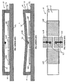
- FIG. 8 illustrates a MEMS switch.
- FIG. 9 is a top view of the MEMS switch shown FIG. 8 with portions removed and portions shown in phantom.
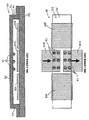
- FIG. 10 illustrates another MEMS switch.
- FIG. 11 is a top view of the MEMS switch shown FIG. 10 with portions removed and portions shown in phantom.
- FIG. 12 illustrates another MEMS switch.
- FIG. 13 is a top view of the MEMS switch shown FIG. 12 with portions removed and portions shown in phantom.
- FIG. 14 is a block diagram of an electronic system incorporating at least one MEMS switch.
- In the following detailed description reference is made to the accompanying drawings in which is shown by way of illustration specific embodiments. These embodiments are described in sufficient detail to enable those skilled in the art to practice the embodiments of invention. Other embodiments may be utilized and/or changes made to the illustrated embodiments.
- FIGS. 8 and 9 show a
MEMS switch 70.MEMS switch 70 includes asubstrate 72 with an upper surface 74. Thesubstrate 72 may be part of a chip or any other electronic device. Anactuation electrode 76 and asignal contact 78 are formed on the upper surface 74 ofsubstrate 72. Theactuation electrode 76 andsignal contact 78 are electrically connected with other electronic components via conducting traces in thesubstrate 72, or through other conventional means. -
Switch 70 further includes abridge beam 80 having aflexible portion 82 supported at both ends bystructural portions 84. It should be noted that in alternative embodiments,beam 80 is suspended oversubstrate 72 in a cantilevered fashion.Beam 80 is suspended overactuation electrode 76 with agap 77 between theactuation electrode 76 andbeam 80.Gap 77 is sized so that theactuation electrode 76 is in electrostatic communication withbeam 80. -
Beam 80 is suspended over at least a portion of thesignal contact 78 such thatgap 77 is also betweenbeam 80 andsignal contact 78. In one embodiment,gap 77 is anywhere from 0.5 to 2 microns. -
MEMS switch 80 operates by applying a voltage toactuation electrode 76. The voltage creates an attractive electrostatic force betweenactuation electrode 76 andbeam 80 that deflectsbeam 80 toward theactuation electrode 76.Beam 80 moves towardsubstrate 72 untilprotuberances 81 onbeam 80 engagesignal contact 78 to establish an electrical connection betweenbeam 80 andsignal contact 78. In some embodiments,beam 80 engagessignal contact 78 directly. -
Actuation electrode 76 is positioned between at least two portions ofsignal contact 78 such that the attractive force generated byactuation electrode 76 encompasses more of the area surrounding eachprotuberance 81.Actuation electrode 76 is positioned between a first portion and a second portion ofsignal contact 78. Surrounding more of the area around eachprotuberance 81 with the attractive force that is generated byactuation electrode 76 facilitates engaging eachprotuberance 81 withsignal contact 78 during operation ofswitch 70. In addition, thegap 77 betweenactuation electrode 76 andbeam 80 is relatively small such that a relatively low actuation voltage is required to operateswitch 70. - In the sample embodiment illustrated in FIGS. 8 and 9,
signal contact 78 includes aninput contact 85A and anoutput contact 85B. Each of the input andoutput contacts body 86 withprojections 87 extending from therespective bodies 86.Projections 87 are positioned underbeam 80 in alignment withprotuberances 81. -
Actuation electrode 76 includesouter pads 90 that are positioned underbeam 80 on both sides ofsignal contact 78. Theouter pads 90 are connected by aninner pad 91 that extends betweenprojections 87 on input andoutput contacts - Although input and
output contacts projections 87 extending from eachbody 86 any number of projections may extend from thebodies 86. In addition, in some embodiments projections may extend from only onebody 86. - FIGS. 10 and 11 illustrate another
MEMS switch 100.MEMS switch 100 includes abeam 110 that is similar tobeam 80 described above. Asignal contact 102 is mounted onto anupper surface 103 of asubstrate 104. The signal contact includes aninput contact 106 and anoutput contact 108. The input andoutput contacts segments 107 that are at least partly positioned belowbeam 110. -
Beam 110 is electrostatically deflected by anactuation electrode 112 so thatprotuberances 113 onbeam 110 engagesegments 107 onsignal contact 102 to establish an electrical connection betweenbeam 110 andsignal contact 102. Whenbeam 110 is engaged withsignal contact 102,beam 110 serves as a shunt for any electric signal passing throughsignal contact 102.Actuation electrode 112 includes inner pads 114B that are each positioned between pairs ofsegments 107 onsignal contact 102, andouter pads 114A that are positionedoutside segments 107. In other example embodiments,signal contact 102 includes two segments andactuation electrode 112 includes a single pad between the two segments. - Inner and
outer pads 114A, 114B are electrically coupled together by a connectingpad 115 that is positioned belowupper surface 103 ofsubstrate 104.Connecting pad 115 extends below inner andouter pads 114A, 114B andsegments 107.Vias 116 electricallycouple connecting pad 115 to inner andouter pads 114A, 114B. Since connectingpad 115 is also positioned belowbeam 110, connectingpad 115 supplements the actuating force applied by the inner andouter pads 114A, 114B during operation ofMEMS switch 100. - FIGS. 12 and 13 illustrate another
MEMS switch 130.MEMS switch 130 includes abeam 140 that is similar tobeams signal contact 132 is mounted onto anupper surface 133 ofsubstrate 134.Signal contact 132 includes aninput contact 136 and anoutput contact 138. Input andoutput contacts segments 137 that are at least partly positioned belowbeam 110. -
Beam 140 is electrostatically deflected by anactuation electrode 142 so thatbeam 140 directly engagessignal contact 132 to establish an electrical connection betweenbeam 140 andsignal contact 132.Actuation electrode 142 includesouter pads 144A that are positionedoutside segments 137 andinner pads 144B that are each positioned between a unique pair ofsegments 137 onsignal contact 132. - Inner and
outer pads pad 145 that is positioned belowupper surface 133 ofsubstrate 134.Inner pads 144B are only partially positioned betweensegments 137 becausesegments 137 are raised slightly above the level ofpads segments 137 insignal contact 132 are slightly abovepads actuation electrode 142, there is no need for protuberances to placed onbeam 140. - Input and
output contacts outer pads dielectric layer 149. Addingdielectric layer 149 is especially effective whenMEMS switch 130 is acting as a high frequency capacitive shunt switch. In other example embodiments,dielectric layer 149 may cover only a portion ofsignal contact 132 and/oractuation electrode 142. - In any embodiment, the height of any actuation electrode may be less than that of any signal contact so that the beam does not engage the actuation electrode when the beam is deflected. The actuation electrodes and signal contacts may be arranged perpendicular to the longitudinal axis of the beam, parallel to the longitudinal axis of the beam, or have any configuration that facilitates efficient switching. The beam may also have any shape as long as the shape is adequate for a particular application.
- MEMS switches provide superior power efficiency, low insertion loss and excellent isolation. Any of the MEMS switches or alternatives described above are highly desirable because they are readily integrated onto a substrate that may be part of another device such as filters or CMOS chips. The tight integration of the MEMS switches reduces power loss, parasitics, size and costs.
- FIG. 14 is a block diagram of an
electronic system 150 incorporating at least oneMEMS switch 151, such as MEMS switches 70, 100, 130 illustrated in FIGS. 7-13.Electronic system 150 may be a computer system that includes asystem bus 152 to electrically couple the various components ofelectronic system 150.System bus 152 may be a single bus or any combination of busses. -
MEMS switch 151 may be part of anelectronic assembly 153 that is coupled tosystem 152. In one embodiment,electronic assembly 153 includes aprocessor 156 which can be of any type. As used herein, processor means any type of circuit such as, but not limited to, a microprocessor, a microcontroller, a graphics processor or a digital signal processor. - Other types of circuits that can be included in
electronic assembly 153 are a custom circuit or an application-specific integrated circuit, such ascommunications circuit 157 for use in wireless devices such as cellular telephones, pagers, portable computers, two-way radios, and similar electronic systems. - The
electronic system 150 may also include anexternal memory 160 that in turn may include one or more memory elements suitable to the particular application, such as a main memory 162 in the form of random access memory (RAM), one or morehard drives 164, and/or one or more drives that handleremovable media 166, such as floppy diskettes, compact disks (CDs) and digital video disks (DVDs). - The
electronic system 150 may also include adisplay device 168, aspeaker 169, and acontroller 170, such as a keyboard, mouse, trackball, game controller, microphone, voice-recognition device, or any other device that inputs information into theelectronic system 150. -
MEMS switch 151 can be implemented in a number of different forms, including an electronic package, an electronic system, a computer system, one or more methods of fabricating an electronic package, and one or more methods of fabricating an electronic assembly that includes the package. - FIGS. 7-13 are representational and are not necessarily drawn to scale. Certain proportions thereof may be exaggerated, while others may be minimized.
Claims (20)
- A MEMS switch comprising:a signal contact (78) including a first portion and a second portion;an actuation electrode (76, 112, 142) positioned between the first and second portions of the signal contact; anda beam (80, 110, 140) that engages the signal contact when a voltage is applied to the actuation electrode; whereinthe signal contact includes an input contact (85A, 106, 136) as first portion and an output contact (858, 108, 138) as second portion; andthe input contact is connected to the output contact by the beam when a voltage is applied to the actuation electrode; characterised in thatat least one of the input and output contacts includes a body and projections (87) extending from the body with the projections positioned under the beam, the actuation electrode being positioned between the projections.
- The MEMS switch of claim 1, wherein the beam is a bridge beam.
- The MEMS switch of claim 1, wherein the beam includes a plurality of protuberances that engage the signal contact.
- The MEMS switch of claim 1, wherein each of the input and output contacts includes a body and projections extending from the respective bodies with the projections positioned under the beam, the actuation electrode being positioned between the projections on the input and output contacts.
- The MEMS switch of claim 1, wherein the input contact is electrically connected to the output contact by two segments and the actuation electrode is positioned between the segments.
- The MEMS switch of claim 1, wherein the input contact is electrically connected to the output contact by a plurality of segments, and the actuation electrode includes a plurality of electrically connected pads, each pad on the actuation electrode being positioned between a unique pair of segments on the signal contact.
- The MEMS switch of claim 1, wherein the actuation electrode (76, 112, 142) includes an inner pad (91,114A, 144B) positioned between the first and second portions of the signal contact and at least one outer pad (90,114B, 144A) positioned outside the first and second portions of the signal contact.
- The MEMS switch of claim 7, wherein the pads of the actuation electrode are under the beam.
- The MEMS switch of claim 7, wherein the inner pad is electrically connected to each outer pad.
- The MEMS switch of claim 9, further comprising a substrate, wherein the signal contact and the inner and outer pads are mounted on a surface of the substrate.
- The MEMS switch of claim 10, wherein the inner and outer pads are electrically coupled by a connecting pad (115,145) positioned below the surface of the substrate.
- The MEMS switch of claim 11, wherein the inner and outer pads are electrically connected to the connecting pad by vias (116).
- The MEMS switch of claim 1, wherein the signal contact is covered with a dielectric layer that engages the beam when a voltage is applied to the actuation electrode.
- The MEMS switch of claim 13, wherein the actuation electrode is covered with a dielectric layer.
- The MEMS switch of claim 1 comprising:a substrate including a surface;said signal contact (78) on the surface the substrate;a bridge beam (80,110,140); andsaid actuation electrode (76,112,142) including an inner pad positioned under the beam and between the first and second portions of the signal contact, at least one outer pad positioned under the beam and outside the first and second portions of the signal contact, and a connecting pad positioned below the surface of the substrate to electrically connect the inner and outer pads; whereinthe beam includes a plurality of protuberances to engage the signal contact when a voltage is applied to the actuation electrode.
- The MEMS switch of claim 15, wherein the signal contact includes an input contact and an output contact that is connected to the input contact by the beam when a voltage is applied to the actuation electrode.
- The MEMS switch of claim 15, wherein the signal contact includes an input contact and an output contact that is electrically connected to the input contact by a plurality of segments.
- A computer system comprising; a bus;
a memory coupled to the bus;
an electronic assembly connected to the bus, the electronic assembly including the MEMS switch of claim 1. - The system of claim 18, wherein the actuation electrode and signal contact are covered with a dielectric layer.
- The system of claim 18, wherein the beam is a bridge beam.
Applications Claiming Priority (3)
| Application Number | Priority Date | Filing Date | Title |
|---|---|---|---|
| US10/219,013 US6850133B2 (en) | 2002-08-14 | 2002-08-14 | Electrode configuration in a MEMS switch |
| US219013 | 2002-08-14 | ||
| PCT/US2003/025360 WO2004017350A1 (en) | 2002-08-14 | 2003-08-13 | Electrode configuration in a mems switch |
Publications (2)
| Publication Number | Publication Date |
|---|---|
| EP1529300A1 EP1529300A1 (en) | 2005-05-11 |
| EP1529300B1 true EP1529300B1 (en) | 2007-11-21 |
Family
ID=31714652
Family Applications (1)
| Application Number | Title | Priority Date | Filing Date |
|---|---|---|---|
| EP03751854A Expired - Lifetime EP1529300B1 (en) | 2002-08-14 | 2003-08-13 | Electrode configuration in a mems switch |
Country Status (9)
| Country | Link |
|---|---|
| US (2) | US6850133B2 (en) |
| EP (1) | EP1529300B1 (en) |
| JP (1) | JP4076536B2 (en) |
| CN (1) | CN1842884B (en) |
| AU (1) | AU2003269961A1 (en) |
| DE (1) | DE60317680D1 (en) |
| MY (1) | MY134267A (en) |
| TW (1) | TWI307676B (en) |
| WO (1) | WO2004017350A1 (en) |
Cited By (1)
| Publication number | Priority date | Publication date | Assignee | Title |
|---|---|---|---|---|
| EP2148350A2 (en) | 2008-07-24 | 2010-01-27 | General Electric Company | Low work function electrical component |
Families Citing this family (61)
| Publication number | Priority date | Publication date | Assignee | Title |
|---|---|---|---|---|
| US7166910B2 (en) * | 2000-11-28 | 2007-01-23 | Knowles Electronics Llc | Miniature silicon condenser microphone |
| US7439616B2 (en) | 2000-11-28 | 2008-10-21 | Knowles Electronics, Llc | Miniature silicon condenser microphone |
| US8623709B1 (en) | 2000-11-28 | 2014-01-07 | Knowles Electronics, Llc | Methods of manufacture of top port surface mount silicon condenser microphone packages |
| US7434305B2 (en) | 2000-11-28 | 2008-10-14 | Knowles Electronics, Llc. | Method of manufacturing a microphone |
| US6791441B2 (en) * | 2002-05-07 | 2004-09-14 | Raytheon Company | Micro-electro-mechanical switch, and methods of making and using it |
| JP4206856B2 (en) * | 2002-07-30 | 2009-01-14 | パナソニック株式会社 | Switch and switch manufacturing method |
| US6781231B2 (en) * | 2002-09-10 | 2004-08-24 | Knowles Electronics Llc | Microelectromechanical system package with environmental and interference shield |
| US8732644B1 (en) | 2003-09-15 | 2014-05-20 | Nvidia Corporation | Micro electro mechanical switch system and method for testing and configuring semiconductor functional circuits |
| US8775997B2 (en) * | 2003-09-15 | 2014-07-08 | Nvidia Corporation | System and method for testing and configuring semiconductor functional circuits |
| US8788996B2 (en) | 2003-09-15 | 2014-07-22 | Nvidia Corporation | System and method for configuring semiconductor functional circuits |
| US8507277B2 (en) | 2003-10-24 | 2013-08-13 | Gencia Corporation | Nonviral vectors for delivering polynucleotides |
| US8133733B2 (en) | 2003-10-24 | 2012-03-13 | Gencia Corporation | Nonviral vectors for delivering polynucleotides to target tissues |
| US8062891B2 (en) | 2003-10-24 | 2011-11-22 | Gencia Corporation | Nonviral vectors for delivering polynucleotides to plants |
| CA2543257C (en) | 2003-10-24 | 2013-12-31 | Gencia Corporation | Methods and compositions for delivering polynucleotides |
| US20090123468A1 (en) | 2003-10-24 | 2009-05-14 | Gencia Corporation | Transducible polypeptides for modifying metabolism |
| US6880940B1 (en) * | 2003-11-10 | 2005-04-19 | Honda Motor Co., Ltd. | Magnesium mirror base with countermeasures for galvanic corrosion |
| US8711161B1 (en) | 2003-12-18 | 2014-04-29 | Nvidia Corporation | Functional component compensation reconfiguration system and method |
| US7307331B2 (en) * | 2004-03-31 | 2007-12-11 | Intel Corporation | Integrated radio front-end module with embedded circuit elements |
| US7312505B2 (en) * | 2004-03-31 | 2007-12-25 | Intel Corporation | Semiconductor substrate with interconnections and embedded circuit elements |
| US8723231B1 (en) * | 2004-09-15 | 2014-05-13 | Nvidia Corporation | Semiconductor die micro electro-mechanical switch management system and method |
| CN1755477B (en) * | 2004-09-27 | 2011-11-16 | 高通Mems科技公司 | Interferometric modulator array display device with integrated MEMS electrical switches, and method therefor |
| US8711156B1 (en) | 2004-09-30 | 2014-04-29 | Nvidia Corporation | Method and system for remapping processing elements in a pipeline of a graphics processing unit |
| DE102005008514B4 (en) * | 2005-02-24 | 2019-05-16 | Tdk Corporation | Microphone membrane and microphone with the microphone membrane |
| DE102005008512B4 (en) | 2005-02-24 | 2016-06-23 | Epcos Ag | Electrical module with a MEMS microphone |
| DE102005008511B4 (en) * | 2005-02-24 | 2019-09-12 | Tdk Corporation | MEMS microphone |
| JP2006269127A (en) * | 2005-03-22 | 2006-10-05 | Toshiba Corp | Micromachine switch and electronic equipment |
| US8021193B1 (en) | 2005-04-25 | 2011-09-20 | Nvidia Corporation | Controlled impedance display adapter |
| US7531751B2 (en) * | 2005-04-26 | 2009-05-12 | Kabushiki Kaisha Toshiba | Method and system for an improved package substrate for use with a semiconductor package |
| US7793029B1 (en) | 2005-05-17 | 2010-09-07 | Nvidia Corporation | Translation device apparatus for configuring printed circuit board connectors |
| US7243833B2 (en) * | 2005-06-30 | 2007-07-17 | Intel Corporation | Electrically-isolated interconnects and seal rings in packages using a solder preform |
| JP4489651B2 (en) * | 2005-07-22 | 2010-06-23 | 株式会社日立製作所 | Semiconductor device and manufacturing method thereof |
| DE102005053767B4 (en) * | 2005-11-10 | 2014-10-30 | Epcos Ag | MEMS microphone, method of manufacture and method of installation |
| DE102005053765B4 (en) * | 2005-11-10 | 2016-04-14 | Epcos Ag | MEMS package and method of manufacture |
| US8093968B2 (en) * | 2005-11-24 | 2012-01-10 | Panasonic Corporation | Microelectromechanical element and electromechanical switch using the same |
| US8412872B1 (en) | 2005-12-12 | 2013-04-02 | Nvidia Corporation | Configurable GPU and method for graphics processing using a configurable GPU |
| US8417838B2 (en) | 2005-12-12 | 2013-04-09 | Nvidia Corporation | System and method for configurable digital communication |
| US20070235501A1 (en) * | 2006-03-29 | 2007-10-11 | John Heck | Self-packaging MEMS device |
| EP2327768B1 (en) | 2006-04-03 | 2015-09-09 | Promega Corporation | Permuted and nonpermuted luciferase biosensors |
| FR2901917B1 (en) * | 2006-05-31 | 2008-12-19 | Thales Sa | CIRCULATOR RADIO FREQUENCY OR HYPERFREQUENCY |
| US20080042223A1 (en) * | 2006-08-17 | 2008-02-21 | Lu-Lee Liao | Microelectromechanical system package and method for making the same |
| US20080075308A1 (en) * | 2006-08-30 | 2008-03-27 | Wen-Chieh Wei | Silicon condenser microphone |
| US20080083957A1 (en) * | 2006-10-05 | 2008-04-10 | Wen-Chieh Wei | Micro-electromechanical system package |
| US7894622B2 (en) | 2006-10-13 | 2011-02-22 | Merry Electronics Co., Ltd. | Microphone |
| ITMI20070099A1 (en) | 2007-01-24 | 2008-07-25 | St Microelectronics Srl | ELECTRONIC DEVICE INCLUDING DIFFERENTIAL SENSOR DEVICES MEMS AND SUBSTRATES LAUNDRY |
| US7583169B1 (en) | 2007-03-22 | 2009-09-01 | The United States Of America As Represented By The Administrator Of The National Aeronautics And Space Administration | MEMS switches having non-metallic crossbeams |
| US8724483B2 (en) | 2007-10-22 | 2014-05-13 | Nvidia Corporation | Loopback configuration for bi-directional interfaces |
| JP2010061976A (en) * | 2008-09-03 | 2010-03-18 | Toshiba Corp | Switch and esd protection element |
| US20100156577A1 (en) * | 2008-12-22 | 2010-06-24 | General Electric Company | Micro-electromechanical system switch |
| US8687639B2 (en) * | 2009-06-04 | 2014-04-01 | Nvidia Corporation | Method and system for ordering posted packets and non-posted packets transfer |
| EP2320444A1 (en) * | 2009-11-09 | 2011-05-11 | Nxp B.V. | MEMS Switch |
| US9176909B2 (en) | 2009-12-11 | 2015-11-03 | Nvidia Corporation | Aggregating unoccupied PCI-e links to provide greater bandwidth |
| US9331869B2 (en) | 2010-03-04 | 2016-05-03 | Nvidia Corporation | Input/output request packet handling techniques by a device specific kernel mode driver |
| CN102064041B (en) * | 2010-12-16 | 2013-04-03 | 东南大学 | Normally-off state field emission type radio frequency micromechanical switch |
| US9120667B2 (en) | 2011-06-20 | 2015-09-01 | International Business Machines Corporation | Micro-electro-mechanical system (MEMS) and related actuator bumps, methods of manufacture and design structures |
| EP2774390A4 (en) | 2011-11-04 | 2015-07-22 | Knowles Electronics Llc | INTEGRATED DIELECTRIC MEMBRANE FOR SERVING A BARRIER IN AN ACOUSTIC DEVICE, AND METHOD FOR MANUFACTURING THE SAME |
| US9330031B2 (en) | 2011-12-09 | 2016-05-03 | Nvidia Corporation | System and method for calibration of serial links using a serial-to-parallel loopback |
| US9078063B2 (en) | 2012-08-10 | 2015-07-07 | Knowles Electronics, Llc | Microphone assembly with barrier to prevent contaminant infiltration |
| DE102013106353B4 (en) * | 2013-06-18 | 2018-06-28 | Tdk Corporation | Method for applying a structured coating to a component |
| TWI567769B (en) * | 2015-06-30 | 2017-01-21 | Press the sensing device | |
| US9794661B2 (en) | 2015-08-07 | 2017-10-17 | Knowles Electronics, Llc | Ingress protection for reducing particle infiltration into acoustic chamber of a MEMS microphone package |
| US20220293382A1 (en) * | 2021-03-12 | 2022-09-15 | Qorvo Us, Inc. | Mems switch with beam contact portion continuously extending between input and output terminal electrodes |
Family Cites Families (19)
| Publication number | Priority date | Publication date | Assignee | Title |
|---|---|---|---|---|
| GB9309327D0 (en) * | 1993-05-06 | 1993-06-23 | Smith Charles G | Bi-stable memory element |
| US5638946A (en) * | 1996-01-11 | 1997-06-17 | Northeastern University | Micromechanical switch with insulated switch contact |
| US5880921A (en) * | 1997-04-28 | 1999-03-09 | Rockwell Science Center, Llc | Monolithically integrated switched capacitor bank using micro electro mechanical system (MEMS) technology |
| US5953215A (en) * | 1997-12-01 | 1999-09-14 | Karabatsos; Chris | Apparatus and method for improving computer memory speed and capacity |
| JP3852224B2 (en) | 1998-10-08 | 2006-11-29 | オムロン株式会社 | Electrostatic micro relay |
| JP3087741B2 (en) * | 1998-11-04 | 2000-09-11 | 日本電気株式会社 | Micro machine switch |
| JP3796988B2 (en) * | 1998-11-26 | 2006-07-12 | オムロン株式会社 | Electrostatic micro relay |
| US6143997A (en) * | 1999-06-04 | 2000-11-07 | The Board Of Trustees Of The University Of Illinois | Low actuation voltage microelectromechanical device and method of manufacture |
| US6307452B1 (en) * | 1999-09-16 | 2001-10-23 | Motorola, Inc. | Folded spring based micro electromechanical (MEM) RF switch |
| US6496612B1 (en) * | 1999-09-23 | 2002-12-17 | Arizona State University | Electronically latching micro-magnetic switches and method of operating same |
| US6376787B1 (en) * | 2000-08-24 | 2002-04-23 | Texas Instruments Incorporated | Microelectromechanical switch with fixed metal electrode/dielectric interface with a protective cap layer |
| US6504118B2 (en) * | 2000-10-27 | 2003-01-07 | Daniel J Hyman | Microfabricated double-throw relay with multimorph actuator and electrostatic latch mechanism |
| US6621387B1 (en) * | 2001-02-23 | 2003-09-16 | Analatom Incorporated | Micro-electro-mechanical systems switch |
| US6646215B1 (en) * | 2001-06-29 | 2003-11-11 | Teravicin Technologies, Inc. | Device adapted to pull a cantilever away from a contact structure |
| US6529093B2 (en) * | 2001-07-06 | 2003-03-04 | Intel Corporation | Microelectromechanical (MEMS) switch using stepped actuation electrodes |
| US20030080839A1 (en) * | 2001-10-31 | 2003-05-01 | Wong Marvin Glenn | Method for improving the power handling capacity of MEMS switches |
| JP4045090B2 (en) | 2001-11-06 | 2008-02-13 | オムロン株式会社 | Adjustment method of electrostatic actuator |
| US6717496B2 (en) * | 2001-11-13 | 2004-04-06 | The Board Of Trustees Of The University Of Illinois | Electromagnetic energy controlled low actuation voltage microelectromechanical switch |
| US6657525B1 (en) * | 2002-05-31 | 2003-12-02 | Northrop Grumman Corporation | Microelectromechanical RF switch |
-
2002
- 2002-08-14 US US10/219,013 patent/US6850133B2/en not_active Expired - Fee Related
-
2003
- 2003-07-22 TW TW092119929A patent/TWI307676B/en not_active IP Right Cessation
- 2003-07-30 MY MYPI20032863A patent/MY134267A/en unknown
- 2003-08-13 EP EP03751854A patent/EP1529300B1/en not_active Expired - Lifetime
- 2003-08-13 DE DE60317680T patent/DE60317680D1/en not_active Expired - Lifetime
- 2003-08-13 WO PCT/US2003/025360 patent/WO2004017350A1/en not_active Ceased
- 2003-08-13 CN CN038192861A patent/CN1842884B/en not_active Expired - Fee Related
- 2003-08-13 AU AU2003269961A patent/AU2003269961A1/en not_active Abandoned
- 2003-08-13 JP JP2004529363A patent/JP4076536B2/en not_active Expired - Fee Related
-
2004
- 2004-10-22 US US10/971,793 patent/US6972650B2/en not_active Expired - Lifetime
Cited By (1)
| Publication number | Priority date | Publication date | Assignee | Title |
|---|---|---|---|---|
| EP2148350A2 (en) | 2008-07-24 | 2010-01-27 | General Electric Company | Low work function electrical component |
Also Published As
| Publication number | Publication date |
|---|---|
| CN1842884A (en) | 2006-10-04 |
| US6850133B2 (en) | 2005-02-01 |
| US20040032705A1 (en) | 2004-02-19 |
| WO2004017350A1 (en) | 2004-02-26 |
| MY134267A (en) | 2007-11-30 |
| US20050083158A1 (en) | 2005-04-21 |
| JP4076536B2 (en) | 2008-04-16 |
| CN1842884B (en) | 2010-12-15 |
| TWI307676B (en) | 2009-03-21 |
| JP2005536029A (en) | 2005-11-24 |
| TW200404734A (en) | 2004-04-01 |
| US6972650B2 (en) | 2005-12-06 |
| EP1529300A1 (en) | 2005-05-11 |
| DE60317680D1 (en) | 2008-01-03 |
| AU2003269961A1 (en) | 2004-03-03 |
Similar Documents
| Publication | Publication Date | Title |
|---|---|---|
| EP1529300B1 (en) | Electrode configuration in a mems switch | |
| JP3538109B2 (en) | Micro machine switch | |
| US6153839A (en) | Micromechanical switching devices | |
| US6529093B2 (en) | Microelectromechanical (MEMS) switch using stepped actuation electrodes | |
| CN1316525C (en) | Variable capacitance capacitor device | |
| US6621135B1 (en) | Microrelays and microrelay fabrication and operating methods | |
| EP1391906B1 (en) | Electrostatic RF mems switches | |
| EP2398028A2 (en) | Mems switching array having a substrate arranged to conduct switching current | |
| US20070024403A1 (en) | MEMS switch actuated by the electrostatic force and piezoelectric force | |
| CN102290289B (en) | Electrostatically actuated micro-mechanical switching device | |
| JP2010147022A (en) | Micro-electromechanical system switch | |
| US20090026880A1 (en) | Micromechanical device with piezoelectric and electrostatic actuation and method therefor | |
| JP2004127871A (en) | Micro relay and method of manufacturing micro relay | |
| CN1848344B (en) | Electrostatic micro-contact circuit breaker, manufacturing method thereof, and device using the same | |
| US6750078B2 (en) | MEMS switch having hexsil beam and method of integrating MEMS switch with a chip | |
| JP4970150B2 (en) | Semiconductor device | |
| CN100521030C (en) | Micro-electromechanical device and module and driving method thereof | |
| JP3725688B2 (en) | Logic unit | |
| KR100493532B1 (en) | Electrostatic bi-directional microelectromechanical actuator | |
| KR101292928B1 (en) | RF MEMS switch | |
| JP5130291B2 (en) | Electromechanical element and electrical equipment using the same | |
| JP4842041B2 (en) | switch | |
| JP3985229B2 (en) | Micro mechanical switch | |
| JP2008041589A (en) | High frequency switch | |
| JP2009054314A (en) | High frequency switch |
Legal Events
| Date | Code | Title | Description |
|---|---|---|---|
| PUAI | Public reference made under article 153(3) epc to a published international application that has entered the european phase |
Free format text: ORIGINAL CODE: 0009012 |
|
| 17P | Request for examination filed |
Effective date: 20050309 |
|
| AK | Designated contracting states |
Kind code of ref document: A1 Designated state(s): AT BE BG CH CY CZ DE DK EE ES FI FR GB GR HU IE IT LI LU MC NL PT RO SE SI SK TR |
|
| AX | Request for extension of the european patent |
Extension state: AL LT LV MK |
|
| DAX | Request for extension of the european patent (deleted) | ||
| 17Q | First examination report despatched |
Effective date: 20050916 |
|
| GRAP | Despatch of communication of intention to grant a patent |
Free format text: ORIGINAL CODE: EPIDOSNIGR1 |
|
| GRAS | Grant fee paid |
Free format text: ORIGINAL CODE: EPIDOSNIGR3 |
|
| GRAA | (expected) grant |
Free format text: ORIGINAL CODE: 0009210 |
|
| AK | Designated contracting states |
Kind code of ref document: B1 Designated state(s): AT BE BG CH CY CZ DE DK EE ES FI FR GB GR HU IE IT LI LU MC NL PT RO SE SI SK TR |
|
| REG | Reference to a national code |
Ref country code: GB Ref legal event code: FG4D |
|
| REG | Reference to a national code |
Ref country code: IE Ref legal event code: FG4D |
|
| REG | Reference to a national code |
Ref country code: CH Ref legal event code: EP |
|
| REF | Corresponds to: |
Ref document number: 60317680 Country of ref document: DE Date of ref document: 20080103 Kind code of ref document: P |
|
| PG25 | Lapsed in a contracting state [announced via postgrant information from national office to epo] |
Ref country code: LI Free format text: LAPSE BECAUSE OF FAILURE TO SUBMIT A TRANSLATION OF THE DESCRIPTION OR TO PAY THE FEE WITHIN THE PRESCRIBED TIME-LIMIT Effective date: 20071121 Ref country code: SE Free format text: LAPSE BECAUSE OF FAILURE TO SUBMIT A TRANSLATION OF THE DESCRIPTION OR TO PAY THE FEE WITHIN THE PRESCRIBED TIME-LIMIT Effective date: 20080221 Ref country code: NL Free format text: LAPSE BECAUSE OF FAILURE TO SUBMIT A TRANSLATION OF THE DESCRIPTION OR TO PAY THE FEE WITHIN THE PRESCRIBED TIME-LIMIT Effective date: 20071121 Ref country code: CH Free format text: LAPSE BECAUSE OF FAILURE TO SUBMIT A TRANSLATION OF THE DESCRIPTION OR TO PAY THE FEE WITHIN THE PRESCRIBED TIME-LIMIT Effective date: 20071121 Ref country code: ES Free format text: LAPSE BECAUSE OF FAILURE TO SUBMIT A TRANSLATION OF THE DESCRIPTION OR TO PAY THE FEE WITHIN THE PRESCRIBED TIME-LIMIT Effective date: 20080304 |
|
| NLV1 | Nl: lapsed or annulled due to failure to fulfill the requirements of art. 29p and 29m of the patents act | ||
| PG25 | Lapsed in a contracting state [announced via postgrant information from national office to epo] |
Ref country code: FI Free format text: LAPSE BECAUSE OF FAILURE TO SUBMIT A TRANSLATION OF THE DESCRIPTION OR TO PAY THE FEE WITHIN THE PRESCRIBED TIME-LIMIT Effective date: 20071121 Ref country code: SI Free format text: LAPSE BECAUSE OF FAILURE TO SUBMIT A TRANSLATION OF THE DESCRIPTION OR TO PAY THE FEE WITHIN THE PRESCRIBED TIME-LIMIT Effective date: 20071121 Ref country code: BG Free format text: LAPSE BECAUSE OF FAILURE TO SUBMIT A TRANSLATION OF THE DESCRIPTION OR TO PAY THE FEE WITHIN THE PRESCRIBED TIME-LIMIT Effective date: 20080221 |
|
| REG | Reference to a national code |
Ref country code: CH Ref legal event code: PL |
|
| PG25 | Lapsed in a contracting state [announced via postgrant information from national office to epo] |
Ref country code: AT Free format text: LAPSE BECAUSE OF FAILURE TO SUBMIT A TRANSLATION OF THE DESCRIPTION OR TO PAY THE FEE WITHIN THE PRESCRIBED TIME-LIMIT Effective date: 20071121 |
|
| PG25 | Lapsed in a contracting state [announced via postgrant information from national office to epo] |
Ref country code: CZ Free format text: LAPSE BECAUSE OF FAILURE TO SUBMIT A TRANSLATION OF THE DESCRIPTION OR TO PAY THE FEE WITHIN THE PRESCRIBED TIME-LIMIT Effective date: 20071121 Ref country code: DK Free format text: LAPSE BECAUSE OF FAILURE TO SUBMIT A TRANSLATION OF THE DESCRIPTION OR TO PAY THE FEE WITHIN THE PRESCRIBED TIME-LIMIT Effective date: 20071121 |
|
| PG25 | Lapsed in a contracting state [announced via postgrant information from national office to epo] |
Ref country code: RO Free format text: LAPSE BECAUSE OF FAILURE TO SUBMIT A TRANSLATION OF THE DESCRIPTION OR TO PAY THE FEE WITHIN THE PRESCRIBED TIME-LIMIT Effective date: 20071121 Ref country code: SK Free format text: LAPSE BECAUSE OF FAILURE TO SUBMIT A TRANSLATION OF THE DESCRIPTION OR TO PAY THE FEE WITHIN THE PRESCRIBED TIME-LIMIT Effective date: 20071121 Ref country code: BE Free format text: LAPSE BECAUSE OF FAILURE TO SUBMIT A TRANSLATION OF THE DESCRIPTION OR TO PAY THE FEE WITHIN THE PRESCRIBED TIME-LIMIT Effective date: 20071121 |
|
| PLBE | No opposition filed within time limit |
Free format text: ORIGINAL CODE: 0009261 |
|
| STAA | Information on the status of an ep patent application or granted ep patent |
Free format text: STATUS: NO OPPOSITION FILED WITHIN TIME LIMIT |
|
| PG25 | Lapsed in a contracting state [announced via postgrant information from national office to epo] |
Ref country code: PT Free format text: LAPSE BECAUSE OF FAILURE TO SUBMIT A TRANSLATION OF THE DESCRIPTION OR TO PAY THE FEE WITHIN THE PRESCRIBED TIME-LIMIT Effective date: 20080421 |
|
| 26N | No opposition filed |
Effective date: 20080822 |
|
| PG25 | Lapsed in a contracting state [announced via postgrant information from national office to epo] |
Ref country code: DE Free format text: LAPSE BECAUSE OF FAILURE TO SUBMIT A TRANSLATION OF THE DESCRIPTION OR TO PAY THE FEE WITHIN THE PRESCRIBED TIME-LIMIT Effective date: 20080222 Ref country code: FR Free format text: LAPSE BECAUSE OF FAILURE TO SUBMIT A TRANSLATION OF THE DESCRIPTION OR TO PAY THE FEE WITHIN THE PRESCRIBED TIME-LIMIT Effective date: 20080905 |
|
| PG25 | Lapsed in a contracting state [announced via postgrant information from national office to epo] |
Ref country code: GR Free format text: LAPSE BECAUSE OF FAILURE TO SUBMIT A TRANSLATION OF THE DESCRIPTION OR TO PAY THE FEE WITHIN THE PRESCRIBED TIME-LIMIT Effective date: 20080222 |
|
| PG25 | Lapsed in a contracting state [announced via postgrant information from national office to epo] |
Ref country code: MC Free format text: LAPSE BECAUSE OF NON-PAYMENT OF DUE FEES Effective date: 20080831 |
|
| PG25 | Lapsed in a contracting state [announced via postgrant information from national office to epo] |
Ref country code: EE Free format text: LAPSE BECAUSE OF FAILURE TO SUBMIT A TRANSLATION OF THE DESCRIPTION OR TO PAY THE FEE WITHIN THE PRESCRIBED TIME-LIMIT Effective date: 20071121 |
|
| PG25 | Lapsed in a contracting state [announced via postgrant information from national office to epo] |
Ref country code: CY Free format text: LAPSE BECAUSE OF FAILURE TO SUBMIT A TRANSLATION OF THE DESCRIPTION OR TO PAY THE FEE WITHIN THE PRESCRIBED TIME-LIMIT Effective date: 20071121 Ref country code: IE Free format text: LAPSE BECAUSE OF NON-PAYMENT OF DUE FEES Effective date: 20080813 |
|
| PGFP | Annual fee paid to national office [announced via postgrant information from national office to epo] |
Ref country code: GB Payment date: 20090812 Year of fee payment: 7 |
|
| PG25 | Lapsed in a contracting state [announced via postgrant information from national office to epo] |
Ref country code: HU Free format text: LAPSE BECAUSE OF FAILURE TO SUBMIT A TRANSLATION OF THE DESCRIPTION OR TO PAY THE FEE WITHIN THE PRESCRIBED TIME-LIMIT Effective date: 20080522 Ref country code: LU Free format text: LAPSE BECAUSE OF NON-PAYMENT OF DUE FEES Effective date: 20080813 |
|
| PG25 | Lapsed in a contracting state [announced via postgrant information from national office to epo] |
Ref country code: TR Free format text: LAPSE BECAUSE OF FAILURE TO SUBMIT A TRANSLATION OF THE DESCRIPTION OR TO PAY THE FEE WITHIN THE PRESCRIBED TIME-LIMIT Effective date: 20071121 |
|
| PG25 | Lapsed in a contracting state [announced via postgrant information from national office to epo] |
Ref country code: IT Free format text: LAPSE BECAUSE OF NON-PAYMENT OF DUE FEES Effective date: 20080831 |
|
| GBPC | Gb: european patent ceased through non-payment of renewal fee |
Effective date: 20100813 |
|
| PG25 | Lapsed in a contracting state [announced via postgrant information from national office to epo] |
Ref country code: GB Free format text: LAPSE BECAUSE OF NON-PAYMENT OF DUE FEES Effective date: 20100813 |