JP4206856B2 - Switch and switch manufacturing method - Google Patents
Switch and switch manufacturing method Download PDFInfo
- Publication number
- JP4206856B2 JP4206856B2 JP2003279097A JP2003279097A JP4206856B2 JP 4206856 B2 JP4206856 B2 JP 4206856B2 JP 2003279097 A JP2003279097 A JP 2003279097A JP 2003279097 A JP2003279097 A JP 2003279097A JP 4206856 B2 JP4206856 B2 JP 4206856B2
- Authority
- JP
- Japan
- Prior art keywords
- movable electrode
- electrode
- fixed electrode
- movable
- signal transmission
- Prior art date
- Legal status (The legal status is an assumption and is not a legal conclusion. Google has not performed a legal analysis and makes no representation as to the accuracy of the status listed.)
- Expired - Fee Related
Links
Images


Classifications
-
- H—ELECTRICITY
- H01—ELECTRIC ELEMENTS
- H01H—ELECTRIC SWITCHES; RELAYS; SELECTORS; EMERGENCY PROTECTIVE DEVICES
- H01H59/00—Electrostatic relays; Electro-adhesion relays
- H01H59/0009—Electrostatic relays; Electro-adhesion relays making use of micromechanics
Description
本発明は、ON/OFF時の動作速度を向上させたスイッチとそのスイッチの製造方法に関する。 The present invention relates to a switch with improved operating speed at ON / OFF and a method of manufacturing the switch.
従来における信号のスイッチとしては、例えば非特許文献1が知られており、図25に示すように高抵抗シリコン基板2501上に形成した信号伝達線2502と信号伝送線上に所定の空間を介し配置された可動接地線2503および接地線2504から構成される。このようなスイッチにおいては、図26に示すように可動接地線2503と信号伝達線2502からなる平行平板のキャパシタンス容量間に電圧を印加することで静電力を発生させ可動接地線2503と信号伝達線2502を高誘電体膜2505を介して接触させる。接触により信号伝達線と可動接地線間で形成されるキャパシタ容量が大きくなり、その容量に応じた周波数成分の信号が伝達される。
As a conventional signal switch, for example, Non-Patent
このように可動接地線と信号伝達線間の電圧を制御することで信号伝達線から可動接地線へと信号の伝達の接続ならび切断を制御する事が可能となる。さらに、この方式によればLSIの製造工程と同様の工程で信号のスイッチを形成することができ、トランジスタ等の回路と同じ部分に信号のスイッチを形成することで、周波数特性や小型化に有利なスイッチを形成することが可能となる。 In this way, by controlling the voltage between the movable ground line and the signal transmission line, it is possible to control connection and disconnection of signal transmission from the signal transmission line to the movable ground line. Furthermore, according to this method, a signal switch can be formed in the same process as the LSI manufacturing process, and the signal switch is formed in the same part as a circuit such as a transistor, which is advantageous for frequency characteristics and miniaturization. It is possible to form a simple switch.
信号の接続時、切断時ともに動作速度を向上させる手段として、可動電極を2方向に駆動するためにシーソーの形状を持たせたものも提案されており、例えば、非特許文献2に記されている。図27に示すようにGaAs基板2701上に形成した可動電極2703と引っ張り電極2705または押し電極2706間に電圧を印加することで、可動電極はねじれバネ2707を中心とした回転運動を行う。可動電極2703と引っ張り電極2705間に電圧を印加した場合は接触電極2704は信号線2702に接触する方向に、また、可動電極2703と押し電極2706間に電圧を印加した場合、接触電極2704は信号線2702から離れる方向に動くことで、可動電極2703と接触電極2704からなるキャパシタ容量を変化させることで接触電極2704および信号線2702間の信号を接続および切断制御を行うものである。
As a means for improving the operation speed at the time of signal connection and disconnection, a device having a seesaw shape for driving the movable electrode in two directions has been proposed. For example, it is described in Non-Patent
微少部品を駆動させる方法としては、前記平行平板への電圧印加による静電力の他、凸部と凹部の組み合わせによる櫛歯駆動が知られており、例えば非特許文献3が知られている。図28において、静止櫛形電極2804と可動櫛形電極2805間に電圧を印加することで、ねじればね2802を中心に反射鏡2801に回転運動をさせるものである。
これらのスイッチにおいては、信号伝達時の伝達効率並びに切断時の絶縁性とまた信号の接続切断の高速な動作が要求されている。 In these switches, transmission efficiency at the time of signal transmission, insulation at the time of disconnection, and high-speed operation of signal disconnection are required.
しかしながら、LSIの製造工程と同様の工程でスイッチが形成可能な、信号伝送線上に空間を介し可動接地線を形成する装置の場合、可動電極を駆動する電極が信号伝達線のみであり、信号を信号伝達線から接地線へ切り替える場合には可動接地線と信号伝達線の間に電圧を印加し、駆動力を得ることが可能であるが、接地線へと伝達している信号を切断する場合は、可動接地線を構成する材料の有するバネのたわみが戻ることのみにより動作させていたため、切り替え速度を早くすることは困難である。 However, in the case of a device in which a switch can be formed in the same process as the LSI manufacturing process and a movable ground line is formed on a signal transmission line via a space, the electrode that drives the movable electrode is only the signal transmission line, and the signal is transmitted. When switching from the signal transmission line to the ground line, it is possible to apply a voltage between the movable ground line and the signal transmission line to obtain driving force, but when the signal transmitted to the ground line is disconnected. Is operated only by the return of the spring deflection of the material constituting the movable grounding wire, it is difficult to increase the switching speed.
また、バネ定数の高い材料を用いれば接地線へと伝達している信号を切断する切り替え速度を向上することが可能であるが、トレードオフとして信号伝達線から接地線へと切り替える場合の動作速度が遅くなる、可動接地線と信号伝達線の間に印加する電圧が高くなる等の問題を有していた。 In addition, if a material with a high spring constant is used, it is possible to improve the switching speed at which the signal transmitted to the ground line is cut. However, as a trade-off, the operation speed when switching from the signal transmission line to the ground line is possible. Have a problem that the voltage applied between the movable ground line and the signal transmission line becomes high.
また、信号伝送線上に空間を介し可動接地線を形成するスイッチにおいては、製造工程において信号伝送線の形成後、信号伝送線および可動接地線はエッチングされず該当材料のみエッチングされる犠牲層を正確な膜厚で形成し、しかる後、可動接地線を形成する。さらにその後、信号伝送線および可動接地線間の犠牲層を除去することで所定の空間を正確に形成する工程が一般的である。 In addition, in a switch in which a movable ground line is formed on a signal transmission line through a space, a sacrificial layer in which only the corresponding material is etched without forming the signal transmission line and the movable ground line after the formation of the signal transmission line in the manufacturing process is accurately formed. Then, a movable ground line is formed. Further, a process of accurately forming a predetermined space by removing the sacrificial layer between the signal transmission line and the movable ground line is generally performed thereafter.
このような工程で形成する、信号伝送線上に空間を介し可動接地線を形成するスイッチにおいて、可動接地線上にさらに固定の可動接地線駆動用電極を設ける3層構造とした場合、接地線へと伝達している信号を切断する場合においても、可動接地線を高速に動かすことが可能となる。 In a switch that forms a movable ground line on a signal transmission line through a space formed in such a process, when a three-layer structure in which a fixed movable ground line driving electrode is further provided on the movable ground line, Even when the signal being transmitted is disconnected, the movable ground line can be moved at high speed.
しかしながら、このような3層構造では製造工程において可動接地線の下のみならず可動接地線の上の犠牲層も正確に形成する必要があり、製造工程が複雑になってしまう。さらに、3層構造とした場合、信号伝送線、犠牲層、可動接地線、犠牲層、可動接地線駆動用電極と実際の工程では5層からなる段差が発生し、このような高段差に対してパターン形成などの工程を行うことは実質的に不可能である。 However, in such a three-layer structure, it is necessary to accurately form not only the movable ground line but also the sacrificial layer on the movable ground line in the manufacturing process, which complicates the manufacturing process. Further, in the case of a three-layer structure, a signal transmission line, a sacrificial layer, a movable ground line, a sacrificial layer, a movable ground line driving electrode and a step consisting of five layers are generated in the actual process. It is practically impossible to perform processes such as pattern formation.
またこのように梁構造でスイッチを形成する場合、温度変化によって、応力が変化する。これは梁を構成する材料と、基板を構成する材料の熱膨張係数が異なる場合に生じる。梁の応力が変化すると、梁のばね定数が変化するため、スイッチの応答時間および駆動電圧が変化する。 Further, when the switch is formed with the beam structure in this way, the stress changes due to the temperature change. This occurs when the material constituting the beam and the material constituting the substrate have different thermal expansion coefficients. When the beam stress changes, the spring constant of the beam changes, so that the response time of the switch and the drive voltage change.
また最悪の場合、ジャーナル オブ マイクロエレクトロメカニカルシステム 第11巻第4号 2002年 309ページに記載されているように温度変化により、梁が2μm以上も撓むことが知られている。 In the worst case, as described in Journal of Microelectromechanical System Vol. 11, No. 4, 2002, p. 309, it is known that the beam bends by 2 μm or more due to temperature change.
高速応答化を図るためには、可動電極の駆動距離を所望のアイソレーションを得られる必要最小限の距離にする必要があるが、動作環境の変動を考慮すれば、温度変化により梁が撓む量も考慮して、電極間の距離を余分に長くする必要がある。このため、応答時間が更に遅くなるという課題を有していた。 In order to achieve high-speed response, it is necessary to set the drive distance of the movable electrode to the minimum necessary distance to obtain the desired isolation. However, considering fluctuations in the operating environment, the beam bends due to temperature changes. Considering the amount, it is necessary to make the distance between the electrodes extra long. For this reason, there has been a problem that the response time is further delayed.
一方、シーソー型にした場合、信号電極と接触電極が重なった部分の面積でキャパシタ容量が形成される。 On the other hand, in the case of the seesaw type, the capacitor capacitance is formed by the area of the portion where the signal electrode and the contact electrode overlap.
この容量の大きさにより伝達可能な信号の周波数および伝達効率が決まるため、接触電極の大きさは接続切断制御したい信号により決まり、ある決まった周波数の信号に対して接続、切断の特性を得るためには接触電極の大きさを小さくすることは不可能である。さ
らに可動電極全体の質量は接触電極の質量に加え引っ張り電極および押し電極とのキャパシタ容量も形成する部分も必要となってしまう。その結果、シーソー型の場合、直接信号の接続、切断に関与する部分以外にも電極を形成する必要があり、可動電極全体の質量がより増加してしまう。そのため、より高速な接続、切断動作に対して不利になるという問題を有している。
Since the frequency of the signal that can be transmitted and the transmission efficiency are determined by the size of this capacitance, the size of the contact electrode is determined by the signal to be connected / disconnected, and in order to obtain the characteristics of connection / disconnection for a signal of a certain frequency However, it is impossible to reduce the size of the contact electrode. Furthermore, the mass of the entire movable electrode requires a portion for forming the capacitor capacitance with the tension electrode and the push electrode in addition to the mass of the contact electrode. As a result, in the case of the seesaw type, it is necessary to form an electrode in addition to the part directly involved in signal connection and disconnection, and the mass of the entire movable electrode is further increased. Therefore, there is a problem that it is disadvantageous for higher-speed connection and disconnection operations.
さらに櫛形電極を用いた駆動方式では、基板面内方向に駆動を行うものついては比較的容易に形成が可能であるが、基板垂直方向に駆動するものでは高さ方向に構造物を形成する必要があるため形成工程が複雑になってしまうという問題を有している。 Furthermore, in the driving method using the comb-shaped electrode, it is possible to relatively easily form a device that drives in the in-plane direction of the substrate, but in the case of driving in the substrate vertical direction, it is necessary to form a structure in the height direction. Therefore, there is a problem that the formation process becomes complicated.
本発明の目的は、かかる課題を解決すべく、可動電極の下方向の駆動と上方向の駆動を分離することで、構造物の高さを必要とすることなく、また信号の伝達効率および絶縁性を確保しかつ信号の接続切断の高速な動作を行うスイッチおよびその製造方法を提供することである。 The object of the present invention is to solve such a problem by separating the downward drive and the upward drive of the movable electrode, so that the height of the structure is not required and the signal transmission efficiency and insulation are reduced. It is an object of the present invention to provide a switch capable of ensuring high performance and performing high-speed operation for signal connection and disconnection, and a manufacturing method thereof.
上記課題を解決するために、本発明に係るスイッチは、基板上に固定された細長い矩形板状をなす信号伝達用固定電極と、前記信号伝達用固定電極と所定の空間を介して配された信号を伝達する、細長い矩形板状をなすとともに長手方向両端部を基板上に固定され両持ち梁状に構成された可動電極と、前記可動電極の両側面に所定の空間を介して位置する基板上に固定された可動電極駆動用固定電極と、から構成され、前記可動電極は側面における所定の位置に複数の凸部と凹部を有し、前記可動電極駆動用固定電極は前記可動電極の側面の凸部と凹部にそれぞれ対応した凹部と凸部を有し、前記可動電極の側面に形成された凸部は前記可動電極駆動用固定電極に形成した凹部に取り囲まれるように配置し、かつ前記可動電極駆動用固定電極の凸部は前記可動電極の側面の凹部に取り囲まれるように配置され、前記可動電極駆動用固定電極は、前記可動電極の長辺方向側面の所定の位置に形成する複数の凸部と凹部とに対応した凸部と凹部との形状を有したことを特徴としたものであり、信号伝達用固定電極と可動電極間に電圧を印加することで、信号伝達用固定電極と可動電極間の静電力により可動電極を信号伝達用固定電極と接触させる。可動電極が信号伝達用固定電極に接触することで、可動電極と信号伝達用固定電極間のキャパシタ容量が大きくなり、周波数成分を有する信号は信号伝達用固定電極と可動電極間で接続される。 In order to solve the above-described problems, a switch according to the present invention is disposed on a signal transmission fixed electrode having an elongated rectangular plate shape fixed on a substrate, and the signal transmission fixed electrode via a predetermined space. A movable electrode that transmits a signal, has a long and narrow rectangular plate shape, and has both ends in the longitudinal direction fixed on the substrate and is configured as a doubly supported beam, and a substrate that is positioned on both sides of the movable electrode via a predetermined space A movable electrode driving fixed electrode fixed on the movable electrode, the movable electrode having a plurality of convex portions and concave portions at predetermined positions on the side surface, and the movable electrode driving fixed electrode is disposed on the side surface of the movable electrode. The convex portions formed on the side surfaces of the movable electrode are surrounded by the concave portions formed in the movable electrode driving fixed electrode, and Fixed electrode for movable electrode drive The convex portion is arranged so as to be surrounded by the concave portion on the side surface of the movable electrode, and the movable electrode driving fixed electrode is formed by a plurality of convex portions and concave portions formed at predetermined positions on the side surface in the long side direction of the movable electrode. is obtained by characterized in that have a shape with the corresponding projection and recess, by applying a voltage between the signal transmitting fixed electrode and the movable electrode, electrostatic force between the fixed electrode and the movable electrode for signal transmission Thus, the movable electrode is brought into contact with the signal transmission fixed electrode. When the movable electrode comes into contact with the signal transmission fixed electrode, the capacitance of the capacitor between the movable electrode and the signal transmission fixed electrode is increased, and a signal having a frequency component is connected between the signal transmission fixed electrode and the movable electrode.
また、本発明に係るスイッチは、
前記可動電極の側面に形成された凸部は、前記可動電極の凸部の長さよりも短い距離からなる所定の空間を介して、前記可動電極駆動用固定電極に形成した凹部に取り囲まれるように配置したものであり、信号伝達用固定電極と可動電極間に印加した電圧を0とし、可動電極と可動電極駆動用固定電極間に電圧を印加することで、信号伝達用固定電極に接触している可動電極は可動電極駆動用固定電極との静電力により信号伝達用固定電極から所定の空間を介した位置に移動することで、可動電極と信号伝達用固定電極間のキャパシタ容量が小さくなり、周波数成分を有する信号は信号伝達用固定電極と可動電極間で切断されることで、信号の接続および切断動作を行うという作用を有する。
The switch according to the present invention is
Projections formed on the side surface of the movable electrode via a predetermined space of distance less than the length of the convex portion of the movable electrode, to be surrounded in a recess formed in the movable electrode driving fixed electrode The voltage applied between the fixed electrode for signal transmission and the movable electrode is set to 0, and the voltage is applied between the movable electrode and the fixed electrode for driving the movable electrode, so that the fixed electrode for signal transmission is contacted. The movable electrode is moved from the signal transmission fixed electrode to a position through a predetermined space by electrostatic force with the movable electrode driving fixed electrode, thereby reducing the capacitor capacity between the movable electrode and the signal transmission fixed electrode, A signal having a frequency component is cut between the signal transmission fixed electrode and the movable electrode, thereby having a function of connecting and cutting the signal.
また、本発明に係るスイッチは、前記可動電極駆動用固定電極の凸部が、前記可動電極駆動用固定電極の凸部の長さより短い距離からなる所定の空間を介して前記可動電極の側面の凹部に取り囲まれるように配置したものであり、信号伝達用固定電極と可動電極間に印加した電圧を0とし、可動電極と可動電極駆動用固定電極間に電圧を印加することで、信号伝達用固定電極に接触している可動電極は可動電極駆動用固定電極との静電力により信号伝達用固定電極から所定の空間を介した位置に移動することで、可動電極と信号伝達用固定電極間のキャパシタ容量が小さくなり、周波数成分を有する信号は信号伝達用固定電極と可動電極間で切断されることで、信号の接続および切断動作を行うという作用を有する。 The switch according to the present invention, the convex portion of the movable electrode driving fixed electrode, the side surface of the movable electrode via a predetermined space of less than the length distance of the convex portion of the movable electrode driving fixed electrode It is arranged so as to be surrounded by a recess, and the voltage applied between the signal transmission fixed electrode and the movable electrode is set to 0, and the voltage is applied between the movable electrode and the movable electrode driving fixed electrode, thereby transmitting the signal. The movable electrode in contact with the fixed electrode is moved from the signal transmission fixed electrode to a position through a predetermined space by an electrostatic force with the movable electrode driving fixed electrode, so that the movable electrode and the signal transmission fixed electrode are moved. The capacitance of the capacitor is reduced, and a signal having a frequency component is cut between the signal transmission fixed electrode and the movable electrode, thereby having a function of connecting and disconnecting the signal.
また、本発明に係るスイッチは、
前記可動電極と前記可動電極駆動用固定電極の膜厚が同じであるスイッチで、本来可動電極の膜厚は信号の伝達に障害とならない範囲で薄い方が、質量を小さくすることが可能となり、接続、切断動作の速度を速くするのに有効である。一方、可動電極駆動用固定電極の膜厚は段差を乗り越える部分を有するため、厚い方が強度的に有利となる。しかしながら、可動電極側面の凸部および凹部、可動電極駆動用固定電極凹部および凸部間に電圧を印加することで可動電極に静電力を働かせ可動電極を上方向に駆動する場合、静電力は可動電極底部が固定電極底部より基板側に位置する場合および可動電極上面が固定電極上面より上側に位置する場合に大きな静電引力が発生する。そのため、可動電極とか可動電極駆動用固定電極の膜厚を同じ膜厚とすることで、静電力による可動電極の安定位置を正確に可動電極駆動用固定電極の位置と合わせることが可能となる。
The switch according to the present invention is
In the a thickness of the movable electrode and the movable electrode driving fixed electrode are the same switch, the thickness of the original movable electrode towards thinner within a range that does not interfere the transmission of signals, it is possible to reduce the mass, This is effective for increasing the speed of connection and disconnection. On the other hand, since the film thickness of the movable electrode driving fixed electrode has a portion overcoming the step, the thicker one is advantageous in strength. However, if the electrostatic force is applied to the movable electrode by applying a voltage between the convex and concave portions on the side of the movable electrode, the fixed electrode concave and convex portions for driving the movable electrode, and the movable electrode is driven upward, the electrostatic force is movable. A large electrostatic attractive force is generated when the electrode bottom is located on the substrate side from the fixed electrode bottom and when the upper surface of the movable electrode is located above the upper surface of the fixed electrode. Therefore, by setting the film thickness of the movable electrode or the movable electrode driving fixed electrode to the same film thickness, the stable position of the movable electrode by the electrostatic force can be accurately matched with the position of the movable electrode driving fixed electrode.
また、本発明に係るスイッチは、
前記信号伝達用固定電極は、前記可動電極の長辺方向側面の所定の位置に形成する複数の凸部と凹部とに対応した凸部と凹部との形状を有するものであり、信号伝達用固定電極を前記形状とすることで、可動電極と信号伝達用固定電極間のキャパシタ容量は可動電極側面に形成された複数の凸部の面積分大きくすることが可能となる。一方、可動電極駆動用固定電極の凸部の下部には信号伝達用固定電極が存在しないため、信号伝達用固定電極と可動電極駆動用固定電極間の寄生容量を小さくすることが可能となる。さらに、信号伝達用固定電極に設ける凸部形状の幅が信号伝達用固定電極を流れる信号の周波数と比較して十分高いインピーダンスを持つ場合、信号伝達用固定電極に設けた凸部と凹部は伝達する信号に対して何ら悪影響を与え内にも関わらず、可動電極を下方向に駆動する場合、駆動力を増加させることが可能となる。
The switch according to the present invention is
The signal transmitting fixed electrode, which has the shape of a plurality of convex portions and concave portions and convex portions and concave portions corresponding to the formation at a predetermined position in the long side direction side surface of the movable electrode, the fixed signal transduction By forming the electrode in the above-described shape, the capacitor capacitance between the movable electrode and the signal transmission fixed electrode can be increased by the area of the plurality of convex portions formed on the side surface of the movable electrode. On the other hand, since there is no signal transmission fixed electrode below the convex portion of the movable electrode driving fixed electrode, the parasitic capacitance between the signal transmission fixed electrode and the movable electrode driving fixed electrode can be reduced. Further, when the width of the convex shape provided on the signal transmission fixed electrode has a sufficiently high impedance compared to the frequency of the signal flowing through the signal transmission fixed electrode, the convex portion and the concave portion provided on the signal transmission fixed electrode are transmitted. When the movable electrode is driven in the downward direction, the driving force can be increased despite having any adverse effect on the signal.
また、本発明に係るスイッチは、前記可動電極面は、所定の位置に複数の穴を有するものであり、可動電極に複数の穴を設けることで、スイッチの形成工程において前記穴を通して犠牲層除去を行うことができるため、犠牲層除去を容易に行うことが可能となる。さらに、スイッチを大気圧下で動作させて場合、可動電極駆動時、可動電極と信号伝達用固定電極間の気体の粘性により動作速度が制限されることを防ぐことができ、高速な接続、切断動作が可能となる。 The switch according to the present invention, the movable electrode face, has a plurality of holes at predetermined positions, by providing a plurality of holes in the movable electrode, the sacrificial layer is removed through the hole in the step of forming the switch Therefore, it is possible to easily remove the sacrificial layer. In addition, when the switch is operated under atmospheric pressure, the operating speed can be prevented from being restricted by the gas viscosity between the movable electrode and the signal transmission fixed electrode when the movable electrode is driven, and high-speed connection and disconnection can be achieved. Operation is possible.
また、本発明に係るスイッチは、前記可動電極駆動用固定電極は、所定の位置に複数の穴を有するものであり、下部に犠牲層がある可動電極駆動用固定電極に複数の穴を設けることで、前記穴から犠牲層除去工程が進むことで犠牲層除去工程を容易にし、また大気圧下での動作においても、前記穴から気体の出入りが起こることで高速な接続、切断動作を行うことが可能となる。 The switch according to the present invention, the movable electrode driving fixed electrode, has a plurality of holes in a predetermined position, providing a plurality of holes in the movable electrode driving fixed electrode is sacrificial layer in the lower portion Thus, the sacrificial layer removal process proceeds from the hole to facilitate the sacrificial layer removal process, and even in operation under atmospheric pressure, high-speed connection and disconnection operations are performed by gas entering and exiting from the hole. Is possible.
また、本発明に係るスイッチは、前記可動電極が前記信号伝達用固定電極に接触した場合に、前記可動電極の長辺方向側面の所定の位置に形成された凸部又は凹部は、前記可動電極駆動用固定電極に形成された凹部又は凸部と、垂直方向に重なった部分を有するものであり、可動電極が信号伝達用固定電極に接触した状態においても、可動電極側面に形成された複数の凸部と凹部と、可動電極駆動用固定電極に形成された凹部と凸部は垂直方向に重なった部分を有する構造とすることで、可動電極と可動電極駆動用固定電極間に電圧を印加し、可動電極を信号伝達用固定電極から離す場合、効率よく静電引力を伝えることが可能となる。 The switch according to the present invention, when the movable electrode contacts the fixed electrode the signal transmitting, projections or recesses are formed at predetermined positions in the long side direction side surface of the movable electrode, the movable electrode and concave or convex portions formed on the driving fixed electrode, which has a overlapping portion in the vertical direction, even in a state where the movable electrode contacts the fixed electrode for signal transmission, a plurality of which are formed on the movable electrode side surface A voltage is applied between the movable electrode and the movable electrode driving fixed electrode by having a structure in which the convex portion and the concave portion, and the concave portion and the convex portion formed on the movable electrode driving fixed electrode are overlapped in the vertical direction. When the movable electrode is separated from the signal transmission fixed electrode, the electrostatic attractive force can be transmitted efficiently.
また、本発明に係るスイッチは、前記可動電極の側面の凸部のインピーダンスは、少なくとも複数の凸部以外の可動電極の部分からなるインピーダンスより高いものであり、可動電極が信号伝達用固定電極に接触した状態で、信号伝達用固定電極から可動電極へと信号が流れる場合、信号の一部は可動電極の凸部と可動電極駆動用固定電極の凹部からなるキャパシタンス容量を通して信号が漏れてしまう可能性がある。この漏れる信号の量は信号の周波数とキャパシタンスから計算されるインピーダンスと、可動電極側面の凸部の形状により規定されるインピーダンスの合計からなるインピーダンスにより規定される。一方、可動電極側面の凸部の形状から規定されるインピーダンスは数GHzの高周波帯では凸部の幅が狭いほど一般的にインピーダンスが高いことが知られている。従って、可動電極側面の凸部の幅を狭くし、可動電極側面の凸部におけるインピーダンスを可動電極の凸部以外の部分からなるインピーダンスより高くすることで、可動電極に信号が流れる場合、可動電極の凸部と可動電極駆動用固定電極の凹部からなるキャパシタンス容量を通して信号が漏れてしまい、伝達損失が発生することを少なくすることが可能となる。 The switch according to the present invention, the impedance of the convex portion of the side surface of the movable electrode is one higher than the impedance consisting of part of at least a plurality of movable electrodes other than the convex portion, the fixed electrode is movable electrode signal transduction When a signal flows from the signal transmission fixed electrode to the movable electrode in contact, a part of the signal may leak through the capacitance capacitance formed by the convex portion of the movable electrode and the concave portion of the movable electrode driving fixed electrode. There is sex. The amount of the leaked signal is defined by an impedance that is the sum of the impedance calculated from the frequency and capacitance of the signal and the impedance defined by the shape of the convex portion on the side surface of the movable electrode. On the other hand, it is known that the impedance defined by the shape of the convex portion on the side surface of the movable electrode is generally higher in the high frequency band of several GHz as the width of the convex portion is narrower. Therefore, when the width of the convex portion on the side surface of the movable electrode is narrowed and the impedance at the convex portion on the side surface of the movable electrode is made higher than the impedance of the portion other than the convex portion of the movable electrode, It is possible to reduce the occurrence of transmission loss due to leakage of a signal through a capacitance capacity formed by the convex portion of the first electrode and the concave portion of the movable electrode driving fixed electrode.
また、本発明に係るスイッチは、前記可動電極が前記信号伝達用固定電極と接触している状態から、所定の空間を介して前記信号伝達用固定電極と離れた位置に移動する場合、前記可動電極駆動用固定電極と前記可動電極との間に電圧を印加する時間は、前記可動電極が前記信号伝達用固定電極に接触した状態から、前記可動電極の側面に形成された凸部と前記可動電極駆動用固定電極に形成した凹部とで形成される所定の空間と前記可動電極駆動用固定電極の凸部と前記可動電極側面の凹部とで形成される所定の空間との中でもっとも短い距離の移動に要する時間以下とするものであり、スイッチの接続、切断動作において、可動電極が絶縁保持用酸化膜を介して信号伝達用固定電極と接触している状態から離れた位置に移動する場合、可動電極駆動用固定電極と可動電極間に電圧を印加し、静電力を働かせるのは、可動電極が信号伝達用固定電極に接触した状態から可動電極側面に形成された凸部と可動電極駆動用固定電極に形成した凹部および可動電極駆動用固定電極の凸部と可動電極側面の凹部とにより形成される空間の中で最も距離の短い部分の長さだけ移動するのに要する時間以下とすることで、仮に可動電極が可動電極長辺方向に移動した
場合においても、可動電極と可動電極駆動用固定電極が接触することを防ぐことが可能となる。
The switch according to the present invention, when moving from a state in which the movable electrode is in contact with the signal transmitting fixed electrode, at a position apart from the signal transmitting fixed electrode via a predetermined space, the movable time from said state in which the movable electrode contacts the fixed electrode signal transmitting, the convex portion formed on the side surface of the movable electrode movable for applying a voltage to between the electrode driving fixed electrode and the movable electrode shortest distance in a predetermined space formed by a predetermined space formed between the recess formed on the electrode driving fixed electrode and the protrusion of the movable electrode driving fixed electrode and the concave portion of the movable electrode side surface When the movable electrode moves to a position away from the state where it is in contact with the fixed electrode for signal transmission via the insulating holding oxide film in the connection / disconnection operation of the switch. Yes The voltage is applied between the electrode driving fixed electrode and the movable electrode, and the electrostatic force is applied. The movable electrode is in contact with the signal transmitting fixed electrode and the convex portion formed on the side surface of the movable electrode and the movable electrode driving fixed By not exceeding the time required to move by the length of the shortest part of the space formed by the concave portions formed on the electrodes and the convex portions of the movable electrode driving fixed electrode and the concave portions on the side surfaces of the movable electrodes. Even when the movable electrode moves in the long side direction of the movable electrode, it is possible to prevent the movable electrode and the movable electrode driving fixed electrode from contacting each other.
また、本発明に係るスイッチは、前記可動電極駆動用固定電極と前記可動電極との間に電位圧を与える時間は、前記可動電極が前記可動電極駆動用固定電極と接触するのに必要となる時間以下であるものであり、スイッチの動作において、可動電極が絶縁保持用酸化膜を介して信号伝達用固定電極と接触している状態から、所定の空間を介して信号伝達用固定電極と離れた位置に移動する場合、可動電極駆動用固定電極と可動電極間に電圧を印加するのは可動電極が信号伝達用固定電極に接触した状態から、所定の空間幅になり、さらに次に可動電極が信号伝達用固定電極と接触する必要となるまでの時間とすることで、可動電極と信号伝達用固定電極間に電圧を印加していないにも関わらず、信号伝達用固定電極を通過する信号により可動電極が信号伝達用固定電極と接触することを防ぐことが可能となる。
また、本発明に係るスイッチは、前記可動電極と前記信号伝達用固定電極とに電位差が与えられていない場合は、前記可動電極と前記可動電極駆動用固定電極との間に電位差を与えるものであり、信号伝達用固定電極に大きな信号が入力した場合においても可動電極は切断したままの状態であるため、信号伝達用固定電極を通過する信号により可動電極が信号伝達用固定電極と接触することを防ぐことが可能となる。
また、本発明に係るスイッチは、前記可動電極と前記信号伝達用固定電極とが接触していない場合は、前記可動電極と前記可動電極駆動用固定電極間に静電力を印加するものであり、可動電極は静電力により可動電極駆動用電極に引っ張り上げられているため、温度が変化しても、ギャップが減少しない温度補償機能を有することができる。
In the switch according to the present invention, the time for applying the potential pressure between the movable electrode driving fixed electrode and the movable electrode is necessary for the movable electrode to contact the movable electrode driving fixed electrode. In the operation of the switch, the movable electrode is separated from the signal transmission fixed electrode through a predetermined space from the state in which the movable electrode is in contact with the signal transmission fixed electrode through the insulating holding oxide film. When moving to a fixed position, the voltage is applied between the movable electrode driving fixed electrode and the movable electrode from the state in which the movable electrode is in contact with the signal transmitting fixed electrode, and then the predetermined space width is applied. The signal that passes through the fixed electrode for signal transmission even though no voltage is applied between the movable electrode and the fixed electrode for signal transmission Movable by Pole it is possible to prevent the contact with the signal transmitting fixed electrode.
The switch according to the present invention provides a potential difference between the movable electrode and the movable electrode driving fixed electrode when no potential difference is applied between the movable electrode and the signal transmission fixed electrode. Yes, even when a large signal is input to the signal transmission fixed electrode, the movable electrode remains disconnected, so that the movable electrode comes into contact with the signal transmission fixed electrode by a signal passing through the signal transmission fixed electrode. Can be prevented.
The switch according to the present invention applies an electrostatic force between the movable electrode and the movable electrode driving fixed electrode when the movable electrode and the signal transmission fixed electrode are not in contact with each other. Since the movable electrode is pulled up to the movable electrode driving electrode by an electrostatic force, it can have a temperature compensation function in which the gap does not decrease even if the temperature changes.
また、本発明に係るスイッチは、可動電極と信号伝達用固定電極が接触していない状態で、温度が変化した場合、可動電極と可動電極駆動用固定電極間に静電力を印加するもので、温度変化により内部応力が変化して可動電極が撓み、可動電極と信号伝達用電極間の距離が変化して所望のアイソレーションがとれなくなるため、可動電極と信号伝達用固定電極が接触していない状態においては、常に可動電極と可動電極駆動用固定電極間に静電力を印加しておくことで、可動電極の位置を温度変化によらず常に一定の位置に固定でき、温度補償が可能となる。 The switch according to the present invention applies an electrostatic force between the movable electrode and the movable electrode driving fixed electrode when the temperature changes in a state where the movable electrode and the signal transmission fixed electrode are not in contact with each other. The internal stress changes due to the temperature change and the movable electrode bends, and the distance between the movable electrode and the signal transmission electrode changes, and the desired isolation cannot be obtained, so the movable electrode and the signal transmission fixed electrode are not in contact with each other. In a state, by always applying an electrostatic force between the movable electrode and the movable electrode driving fixed electrode, the position of the movable electrode can always be fixed at a fixed position regardless of the temperature change, and temperature compensation is possible. .
本発明に係るスイッチの製造方法は、基板上にシリコン酸化膜を形成するステップと、前記シリコン酸化膜上に金属を形成するステップと、金属上のシリコン酸化膜をドライエッチングするステップと、金属をエッチングして電極間絶縁保持用シリコン酸化膜を形成するステップと、可動電極と可動電極の側面の凸部と凹部および可動電極駆動用固定電極の凹部と凸部は同一犠牲層上に形成するステップを有することを特徴としており、信号の伝達効率および絶縁性を確保しかつ信号の接続切断の高速な動作を行うことができるスイッチを簡単な工程でスイッチを製造することができる。また、可動電極だけでなく可動電極駆動用固定電極の凹部と凸部および可動電極駆動用固定電極の所定の部分に関しても同一の犠牲層上に形成することで、可動電極および可動電極側面の凸部と凹部および可動電極駆動用固定電極の凹部と凸部の高さを、信号伝達用固定電極からの正確に制御することを可能とする。 The method for manufacturing a switch according to the present invention includes a step of forming a silicon oxide film on a substrate, a step of forming a metal on the silicon oxide film, a step of dry etching the silicon oxide film on the metal, Etching to form a silicon oxide film for insulating between electrodes, and forming the movable electrode and the convex and concave portions of the side surface of the movable electrode and the concave and convex portions of the movable electrode driving fixed electrode on the same sacrificial layer Thus, a switch capable of ensuring signal transmission efficiency and insulation and performing a high-speed operation of signal connection / disconnection can be manufactured through a simple process. Further, not only the movable electrode but also the concave and convex portions of the movable electrode driving fixed electrode and the predetermined portions of the movable electrode driving fixed electrode are formed on the same sacrificial layer, so that the convex portions of the movable electrode and the movable electrode side surface are formed. It is possible to accurately control the heights of the concave portion and the convex portion of the portion, the concave portion and the movable electrode driving fixed electrode from the fixed electrode for signal transmission.
また、本発明に係るスイッチの製造方法は、さらに、可動電極および可動電極駆動用固定電極を配置する場所にレジストマスクを形成するステップと、可動電極および可動電極駆動用固定電極を形成するステップと、レジストマスクおよび犠牲層を除去して容量低減用空間を形成するステップとを有し、可動電極および可動電極駆動用固定電極を簡単に製造することができる。 The switch manufacturing method according to the present invention further includes a step of forming a resist mask at a position where the movable electrode and the movable electrode driving fixed electrode are disposed, and a step of forming the movable electrode and the movable electrode driving fixed electrode. And removing the resist mask and the sacrificial layer to form a capacity reduction space, and the movable electrode and the movable electrode driving fixed electrode can be easily manufactured.
また、本発明に係るスイッチの製造方法は、さらに、犠牲層をポリイミドで形成するステップと、全面にAL膜をスパッタリング法により形成するステップを有するものであり、可動電極および可動電極駆動用固定電極を一層簡単に製造することができる。 The switch manufacturing method according to the present invention further includes a step of forming a sacrificial layer with polyimide and a step of forming an AL film on the entire surface by a sputtering method. The movable electrode and the fixed electrode for driving the movable electrode Can be manufactured more easily.
また、本発明に係るスイッチの製造方法は、可動電極駆動用固定電極の下部の所定の位置に段差緩和用のパターンを形成するものであり、段差緩和用のパターンを形成することで段差緩和用のパターンを形成することで、可動電極駆動用固定電極の一部に極端に膜厚の薄い部分が形成されることを防ぐことが可能となり、可動電極駆動用固定電極の強度不足および断線を防ぐことを可能とする。 The switch manufacturing method according to the present invention forms a step relief pattern at a predetermined position below the movable electrode driving fixed electrode, and the step relief pattern is formed by forming the step relief pattern. By forming this pattern, it becomes possible to prevent an extremely thin portion from being formed on a part of the movable electrode driving fixed electrode, thereby preventing insufficient strength and disconnection of the movable electrode driving fixed electrode. Make it possible.
また、本発明に係るスイッチの製造方法は、信号伝達用固定電極の側面の所定の位置に段差緩和用のパターンを形成するものであり、段差緩和用パターンの形成位置に応じた効果が得られ、信号伝達用固定電極の短辺方向側面に段差緩和用のパターンを形成した場合、可動電極の強度不足、断線を防ぐことが可能となる。さらに、可動電極と信号伝達用固定電極間の空間の距離の正確な制御も可能となる。また、信号伝達用固定電極の長辺方向側面に段差緩和用のパターンを形成した場合、可動電極の側面の凸部と凹部の形状および可動電極駆動用固定電極の凹部と凸部の形状がより微な大きさのパターンまで容易に形成することを可能とする。 The switch manufacturing method according to the present invention forms a step relief pattern at a predetermined position on the side surface of the signal transmission fixed electrode, and an effect corresponding to the formation position of the step relief pattern is obtained. When the step-relief pattern is formed on the side surface in the short side direction of the fixed electrode for signal transmission, it becomes possible to prevent the movable electrode from being insufficient in strength and disconnected. Furthermore, it is possible to accurately control the distance of the space between the movable electrode and the signal transmission fixed electrode. In addition, when a pattern for reducing a step is formed on the side surface in the long side direction of the signal transmission fixed electrode, the shape of the convex portion and the concave portion on the side surface of the movable electrode and the shape of the concave portion and the convex portion on the movable electrode driving fixed electrode are more It is possible to easily form even a fine pattern.
また、本発明に係るスイッチの製造方法は、可動電極と可動電極駆動用固定電極を、同一工程で形成した膜をエッチングすることで可動電極および可動電極駆動用固定電極を形成するものであり、可動電極と可動電極駆動用固定電極の正確な膜厚制御が可能である。さらに、可動電極と可動電極駆動用固定電極を同一のマスクよりエッチング形成することで可動電極側面の凸部と両側に位置する可動電極駆動用固定電極の凹部間の所定空間のずれを最小に押さえることが可能となる。 Moreover, the manufacturing method of the switch according to the present invention is to form the movable electrode and the movable electrode driving fixed electrode by etching the film formed of the movable electrode and the movable electrode driving fixed electrode in the same process, Accurate film thickness control of the movable electrode and the movable electrode driving fixed electrode is possible. Further, by etching the movable electrode and the movable electrode driving fixed electrode from the same mask, a predetermined space shift between the convex portion on the side surface of the movable electrode and the concave portion of the movable electrode driving fixed electrode located on both sides is minimized. It becomes possible.
また、本発明に係るスイッチの製造方法は、可動電極と可動電極駆動用固定電極を同一のメッキ工程で可動電極および可動電極駆動用固定電極を形成するものであり、同一工程で可動電極および可動電極駆動用固定電極を形成することで、膜厚の制御を容易に行うことが可能となる。 In the method for manufacturing a switch according to the present invention, the movable electrode and the movable electrode driving fixed electrode are formed in the same plating step, and the movable electrode and the movable electrode driving fixed electrode are formed in the same step. By forming the electrode driving fixed electrode, the film thickness can be easily controlled.
また、本発明に係るスイッチの製造方法は、可動電極と可動電極側面の凸部と凹部および可動電極駆動用固定電極の凹部と凸部および可動電極駆動用固定電極の所定の部分はレジストからなる犠牲層上に形成するものであり、犠牲層にレジストを用いることで、犠牲層除去工程を酸素プラズマによる犠牲層除去が可能となる。 In the switch manufacturing method according to the present invention, the movable electrode, the convex and concave portions of the movable electrode side surface, and the concave and convex portions of the movable electrode driving fixed electrode and the predetermined portions of the movable electrode driving fixed electrode are made of resist. It is formed on the sacrificial layer. By using a resist for the sacrificial layer, the sacrificial layer can be removed by oxygen plasma in the sacrificial layer removal step.
また、本発明に係るスイッチの製造方法は、可動電極と可動電極側面の凸部と凹部および可動電極駆動用固定電極の凹部と凸部および可動電極駆動用固定電極の所定の部分はポリイミドからなる犠牲層上に形成するものであり、犠牲層にポリイミドを用いることで、酸素プラズマによる犠牲層除去が可能となり、犠牲層除去後の工程で液体中の処理を行う必要がなくなり可動電極と信号伝達用固定電極の吸着を防ぐことが可能となる。さらに、犠牲層にポリイミドを用いた場合、レジストは通常150℃以下の熱処理にしか耐えることができないのに対し、300℃程度の熱処理に耐えることができるため、可動電極ならび可動電極駆動用固定電極の形成時の工程処理温度を高くすることが可能となり、工程の自由度を大きく取ることを可能とする。 In the method for manufacturing a switch according to the present invention, the movable electrode, the convex and concave portions of the side surface of the movable electrode, and the concave and convex portions of the movable electrode driving fixed electrode and the predetermined portions of the movable electrode driving fixed electrode are made of polyimide. The sacrificial layer is formed on the sacrificial layer. By using polyimide for the sacrificial layer, the sacrificial layer can be removed by oxygen plasma, and there is no need to perform processing in the liquid after the sacrificial layer is removed. It is possible to prevent the fixed electrode for adsorption. Furthermore, when polyimide is used for the sacrificial layer, the resist can withstand only heat treatment of 150 ° C. or lower, whereas it can withstand heat treatment of about 300 ° C. Therefore, the movable electrode and the fixed electrode for driving the movable electrode It is possible to increase the process processing temperature at the time of forming the film, and to increase the degree of freedom of the process.
また、本発明に係るスイッチの製造方法は、基板上にシリコン酸化膜を形成するステップと、前記シリコン酸化膜上に金属を形成するステップと、金属上のシリコン酸化膜をドライエッチングするステップと、金属をエッチングして電極間絶縁保持用シリコン酸化膜を形成するステップと、信号伝達用固定電極の側面の所定の位置に段差緩和用パターンを形成するステップを有しており、信号の伝達効率および絶縁性を確保しかつ信号の接続切断の高速な動作を行うことができるスイッチを簡単な工程でスイッチを製造することができる。 The method for manufacturing a switch according to the present invention includes a step of forming a silicon oxide film on a substrate, a step of forming a metal on the silicon oxide film, a step of dry etching the silicon oxide film on the metal, Etching the metal to form a silicon oxide film for interelectrode insulation retention, and forming a step relief pattern at a predetermined position on the side surface of the signal transmission fixed electrode. A switch that can ensure insulation and can perform a high-speed operation for signal disconnection can be manufactured through a simple process.
また、本発明に係るスイッチの製造方法は、さらに、犠牲層を形成するステップと、全面にAL膜をスパッタリング法により形成するステップと、可動電極を形成してから犠牲層および段差緩和用パターンを除去して容量低減用空間を形成するステップとを有するものであり、可動電極および信号伝達用固定電極を簡単に製造することができる。 The switch manufacturing method according to the present invention further includes a step of forming a sacrificial layer, a step of forming an AL film on the entire surface by a sputtering method, a sacrificial layer and a step relief pattern after forming the movable electrode. And a step of forming a capacity reduction space by removing the movable electrode and the fixed electrode for signal transmission can be easily manufactured.
本発明に係る無線回路は、本願発明のスイッチと、信号を増幅する増幅器と、アンテナとを含む無線回路であって、前記スイッチは、前記可動電極を、接地側と接続する対接地接続スイッチとし、前記信号伝達用固定電極を、前記増幅器と前記アンテナとを接続する直列接続スイッチとし、前記直列接続スイッチと前記対接地接続スイッチとを交互に接続、切断することにより信号の入出力制御を行うものであり、信号の伝達経路を信号伝達用固定電極側から可動電極側へと伝達することで、可動電極が信号伝達用固定電極に接触した時、可動電極と可動電極駆動用固定電極間の寄生容量により信号の損失が発生した場合においても損失を最小限に抑えるものである。 A radio circuit according to the present invention is a radio circuit including the switch of the present invention, an amplifier that amplifies a signal, and an antenna , wherein the switch is an anti-ground connection switch that connects the movable electrode to a ground side. , the signal transmitting fixed electrode, and the series connection switch for connecting the said amplifier antenna, connect the series switch and the pair ground connection switch alternately controls input and output of signals by cutting By transmitting the signal transmission path from the signal transmission fixed electrode side to the movable electrode side, when the movable electrode comes into contact with the signal transmission fixed electrode, the movable electrode and the movable electrode driving fixed electrode are Even when a signal loss occurs due to a parasitic capacitance, the loss is minimized.
本発明によれば、可動電極の下方向への駆動は可動電極の下部に位置する信号伝達用固定電極と可動電極の静電力により、一方、可動電極の上方向への駆動は可動電極の長辺方向の両側面に位置する可動電極駆動用固定電極との静電引力により駆動することで、信号の伝達効率および絶縁性を確保しかつ信号の接続切断の高速な動作を行うことができるという効果を有する。さらに、可動電極の側面に可動電極駆動用固定電極を配置することが可能となり、複雑な工程の追加が不要であるという有利な効果が得られる。 According to the present invention, the downward driving of the movable electrode is caused by the electrostatic force of the fixed electrode for signal transmission and the movable electrode located below the movable electrode, while the upward driving of the movable electrode is the length of the movable electrode. By driving by electrostatic attraction with the movable electrode driving fixed electrodes located on both side surfaces in the side direction, signal transmission efficiency and insulation can be secured and high-speed operation of signal disconnection can be performed. Has an effect. Furthermore, the movable electrode driving fixed electrode can be disposed on the side surface of the movable electrode, and an advantageous effect that a complicated process is not required is obtained.
(実施の形態1)
以下本発明の実施の形態1について図面を用いて説明する。
(Embodiment 1)
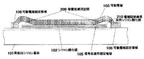
図1は本発明の実施の形態1の場合のスイッチの斜視図である。高抵抗シリコン基板101上のシリコン酸化膜102を介して、可動電極103、可動電極駆動用固定電極104、および信号伝達用固定電極105から構成される。可動電極側面は複数の可動電極側面凸部107を有している。本実施の形態1においては便宜上複数の凸部の形状は全て同じの形状としており、また凸部の配置は周期的に配置している。その結果、1つの可動電極側面凸部と隣接する可動電極側面凸部の間には凹部が形成され、各凹部も周期的に配置されている。一方、可動電極駆動用固定電極凸部108は可動電極側面の凸部と凹部に対応するように配置され、所定の空間を介して可動電極側面の凹部に取り囲まれるように配置されるため、本実施の形態1においては可動電極駆動用固定電極凸部も周期的に配置される構成となる。さらに、可動電極駆動用固定電極の凹部に関しても、可動電極側面の凹部の場合と同様、隣接する凸部間で形成されるため、周期的に配置される。
FIG. 1 is a perspective view of a switch according to
本実施の形態1においては、便宜上、可動電極側面凸部107および可動電極駆動用固定電極凸部の凸部の長さは共に同じ寸法としている。可動電極側面凸部は可動電極駆動用固定電極凹部により可動電極凸部の長さよりも短い距離からなる所定の空間を介して取り囲まれており、また可動電極駆動用固定電極の凸部は可動電極側面の凹部により可動電極駆動用固定電極の凸部の長さよりも短い距離からなる所定の空間を介して取り囲まれているため、図1に示すごとく可動電極側面凸部の一部は可動電極駆動用固定電極凹部の中に、可動電極駆動用固定電極凸部の一部は可動電極凹部の中に入り込むような形に配置される。 In the first embodiment, for convenience, the lengths of the convex portions of the movable electrode side surface convex portion 107 and the movable electrode driving fixed electrode convex portion are the same. The convex part of the movable electrode side surface is surrounded by a movable electrode driving fixed electrode concave part through a predetermined space having a distance shorter than the length of the movable electrode convex part, and the convex part of the movable electrode driving fixed electrode is the movable electrode. Since the concave portion on the side surface is surrounded by a predetermined space having a distance shorter than the length of the convex portion of the movable electrode driving fixed electrode, a part of the convex portion on the side surface of the movable electrode is movable electrode driving as shown in FIG. A portion of the movable electrode driving fixed electrode convex portion is disposed in the movable electrode concave portion so as to enter the movable electrode concave portion.
図2は図1のA−A’断面で、スイッチにおいて信号が信号伝達用固定電極から可動電極への接続がなされていない状態を示した断面図である。高抵抗シリコン基板101上のシリコン酸化膜102を介して信号伝達用固定電極105を配置する。信号伝達用固定電極上には電極間絶縁保持用シリコン酸化膜110が形成されており、さらに容量低減用空間209を介して可動電極103が配置されている。可動電極103は両端の可動電極固定領域106において基板上に固定されている。 FIG. 2 is a cross-sectional view taken along the line A-A ′ of FIG. 1, showing a state where a signal is not connected from the signal transmission fixed electrode to the movable electrode in the switch. A signal transmission fixed electrode 105 is disposed through a silicon oxide film 102 on the high resistance silicon substrate 101. On the signal transmission fixed electrode, an interelectrode insulating holding silicon oxide film 110 is formed, and a movable electrode 103 is arranged through a capacity reduction space 209. The movable electrode 103 is fixed on the substrate in the movable electrode fixed regions 106 at both ends.
図3は図1のB−B’断面で、スイッチにおいて信号が信号伝達用固定電極から可動電極への接続がなされていない状態を示した断面図である。高抵抗シリコン基板101上の
シリコン酸化膜102を介して、可動電極駆動用固定電極104、信号伝達用固定電極105を配置する。信号伝達用固定電極105上には電極間絶縁保持用シリコン酸化膜210が形成されており、さらに容量低減用空間209を介して可動電極103が配置されている。本実施の形態1においては、可動電極駆動用固定電極104の凸部と容量低減用空間209を介した位置での可動電極103の基板表面からの高さが同じになるように設計している。
FIG. 3 is a cross-sectional view taken along the line BB ′ of FIG. 1 and shows a state in which a signal is not connected from the signal transmission fixed electrode to the movable electrode in the switch. A movable electrode driving fixed electrode 104 and a signal transmission fixed electrode 105 are arranged via a silicon oxide film 102 on the high-resistance silicon substrate 101. An interelectrode insulating holding silicon oxide film 210 is formed on the signal transmission fixed electrode 105, and a movable electrode 103 is further disposed via a capacity reduction space 209. In the first embodiment, the height of the movable electrode 103 from the substrate surface at the position through the convex portion of the movable electrode driving fixed electrode 104 and the capacitance reduction space 209 is designed to be the same. .
図4は図1のA−A’断面で、スイッチにおいて信号が信号伝達用固定電極から可動電極へ接続されている状態を示した断面図である。高抵抗シリコン基板101上のシリコン酸化膜102を介して配置された信号伝達用固定電極105と、可動電極103間に電圧を印加することで、静電力により、可動電極103は信号伝達用固定電極105上の電極間絶縁保持用シリコン酸化膜210に接触し、容量低減用空間209は可動電極固定領域近傍に一部残るだけとなる。信号伝達用固定電極105上の電極間絶縁保持用シリコン酸化膜210は、信号伝達用固定電極105と可動電極103間に電圧を印加し、可動電極103が信号伝達用固定電極105に接触した場合においても、信号伝達用固定電極105と可動電極103が直接接触することで電位差が保てなくなり可動電極103が離れてしまうことを防ぐことを目的とする。 FIG. 4 is a cross-sectional view taken along the line A-A ′ of FIG. 1, showing a state where a signal is connected from the signal transmission fixed electrode to the movable electrode in the switch. By applying a voltage between the fixed electrode for signal transmission 105 disposed on the high-resistance silicon substrate 101 via the silicon oxide film 102 and the movable electrode 103, the movable electrode 103 is fixed to the fixed electrode for signal transmission by electrostatic force. The capacitance-reducing space 209 is only partially left in the vicinity of the movable electrode fixed region in contact with the inter-electrode insulating silicon oxide film 210 on 105. The inter-electrode insulating holding silicon oxide film 210 on the signal transmission fixed electrode 105 applies a voltage between the signal transmission fixed electrode 105 and the movable electrode 103, and the movable electrode 103 contacts the signal transmission fixed electrode 105. In this case, the signal transmission fixed electrode 105 and the movable electrode 103 are in direct contact with each other to prevent the potential difference from being maintained and the movable electrode 103 from being separated.
信号伝達用固定電極105と可動電極103により形成される容量は(式1)に従い、電極間絶縁保持用シリコン酸化膜210からなるコンデンサ容量(式2)と容量低減用空間からなるコンデンサ容量(式3)の直列接続容量となる。 The capacitance formed by the signal transmission fixed electrode 105 and the movable electrode 103 is in accordance with (Equation 1), and the capacitor capacitance (Equation 2) composed of the interelectrode insulating holding silicon oxide film 210 and the capacitor capacitance (Equation 2). 3) The series connection capacity.

(式2)および(式3)においてεsはシリコン酸化膜の比誘電率、ε0は真空中の誘電率Sは信号伝達用固定電極105と可動電極103により形成される電極の面積、tは電極間絶縁保持用シリコン酸化膜210の厚さ、dは容量低減用空間209の長さである。また、tは一般的にdの1/10以下の値である。さらに、(式3)は正確には真空中のコンデンサ容量であるが大気中においてもほぼ同等である。可動電極103が信号伝達用固定電極105に接触した場合、容量低減用空間からなるコンデンサ容量は無視できる値となり、電極間絶縁保持用シリコン酸化膜210からなるコンデンサ容量のみと考えて
問題はない。一方、可動電極103が信号伝達用固定電極105から所定の容量低減用空間を保った位置にある場合、コンデンサ容量は容量低減用空間からなるコンデンサ容量が支配的となる。
In (Expression 2) and (Expression 3), εs is the relative permittivity of the silicon oxide film, ε0 is the permittivity in vacuum S is the area of the electrode formed by the signal transmission fixed electrode 105 and the movable electrode 103, and t is the electrode The thickness d of the inter-insulation holding silicon oxide film 210 is the length of the capacity reducing space 209. Further, t is generally a value of 1/10 or less of d. Furthermore, (Equation 3) is precisely the capacitance of the capacitor in a vacuum, but is almost equivalent in the atmosphere. When the movable electrode 103 comes into contact with the signal transmission fixed electrode 105, the capacitor capacity formed by the capacity reducing space becomes a negligible value, and there is no problem considering only the capacitor capacity formed by the inter-electrode insulating holding silicon oxide film 210. On the other hand, when the movable electrode 103 is located at a position where a predetermined capacity reduction space is maintained from the signal transmission fixed electrode 105, the capacitor capacity formed by the capacity reduction space is dominant.
図5は図1のB−B’断面でスイッチにおいて信号が信号伝達用固定電極から可動電極へ接続されている状態を示した断面図である。 FIG. 5 is a cross-sectional view showing a state where a signal is connected from the signal transmission fixed electrode to the movable electrode in the switch in the B-B ′ cross section of FIG. 1.
高抵抗シリコン基板101上のシリコン酸化膜102を介して配置された信号伝達用固定電極105と、可動電極103間に電圧を印加することで、静電力により、可動電極103は信号伝達用固定電極105上の電極間絶縁保持用シリコン酸化膜210に接触し、可動電極駆動用固定電極105と可動電極103間には所定の容量低減用空間分の距離が増加する。 By applying a voltage between the fixed electrode for signal transmission 105 disposed on the high-resistance silicon substrate 101 via the silicon oxide film 102 and the movable electrode 103, the movable electrode 103 is fixed to the fixed electrode for signal transmission by electrostatic force. The distance between the fixed electrode 105 for driving the movable electrode 105 and the movable electrode 103 is increased by a distance corresponding to a predetermined capacity reduction space.
信号伝達用固定電極105から可動電極103へ接続された状態から切断状態への動作は、信号伝達用固定電極105と可動電極103間に印加した電圧を0とし、可動電極103と可動電極駆動用固定電極105間に電圧を印加することで、可動電極駆動用固定電極105と可動電極103間に生じた所定の容量低減用空間分の距離を0とするように静電力が働く。その結果、可動電極103のたわみが戻ろうとするバネの力だけでなく、静電力の両方の力により可動電極103を動かすことで、短時間で信号伝達用固定電極105から離れることが可能となり切断動作特性を向上できるという効果が得られる。 In the operation from the state where the signal transmission fixed electrode 105 is connected to the movable electrode 103 to the disconnected state, the voltage applied between the signal transmission fixed electrode 105 and the movable electrode 103 is set to 0, and the movable electrode 103 and the movable electrode drive are driven. By applying a voltage between the fixed electrodes 105, the electrostatic force acts so that the distance for a predetermined capacity reduction space generated between the movable electrode driving fixed electrode 105 and the movable electrode 103 is zero. As a result, it is possible to move away from the signal transmission fixed electrode 105 in a short time by moving the movable electrode 103 by both the electrostatic force as well as the spring force that the deflection of the movable electrode 103 tries to return. The effect that operational characteristics can be improved is obtained.
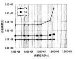
例えば、可動電極103の幅を5μm、長さを400μm、厚みを0.7μmとし、可動電極103と信号伝達用固定電極105とのギャップを0.6μmとした場合の応答特性を図20に示す。図20には、可動電極103と信号伝達用固定電極105が接触した状態から、時刻0で静電力を切り、信号伝達用固定電極105が元の位置の復元する様子を示している。参考のために同じ可動電極103の形状で、櫛歯がない場合も併せて示す。
For example, FIG. 20 shows response characteristics when the width of the movable electrode 103 is 5 μm, the length is 400 μm, the thickness is 0.7 μm, and the gap between the movable electrode 103 and the signal transmission fixed electrode 105 is 0.6 μm. . FIG. 20 shows how the electrostatic force is cut off at
また図21に櫛歯の形状を示す拡大図を示す。櫛歯の形状は、櫛の幅aを1μm、櫛の高さhを5μm、櫛と櫛の間隔を1μmとしている。櫛歯構造がない場合は、可動電極103は、自身が有するばね力のみでもとの位置に復元するため、必然的に応答時間が遅くなる特性であるのに対して、櫛歯構造では、可動電極103と可動電極駆動用固定電極105間に電圧を印加すれば、可動電極103に元の位置に復元する静電力が重畳されるため、より高速な応答が可能となる。 FIG. 21 is an enlarged view showing the shape of the comb teeth. The shape of the comb teeth is such that the width a of the comb is 1 μm, the height h of the comb is 5 μm, and the distance between the combs is 1 μm. When there is no comb-tooth structure, the movable electrode 103 is restored to its original position only by its own spring force, so the response time is inevitably slow. When a voltage is applied between the electrode 103 and the movable electrode driving fixed electrode 105, an electrostatic force that restores the original position is superimposed on the movable electrode 103, so that a faster response is possible.
なお、本実施の形態1においては高抵抗シリコン基板101上にシリコン酸化膜102を介してスイッチの各部品を配置したが、その他の絶縁材料例えばシリコン窒化膜を用いてもよい。また、高抵抗シリコン基板を用いたが、シリコン以外の材料例えばガリウム砒素基板等化合物半導体基板においても、さらに石英、アルミナ等絶縁性基板を用いた場合においても同様の効果が得られる。さらに、基板の抵抗が十分に高く、基板を通して可動電極、信号伝達用固定電極、可動電極駆動用固定電極間の電気的に影響が及ばない場合、シリコン酸化膜もしくは同等の絶縁材料の配置は省略することが可能である。 In the first embodiment, each component of the switch is arranged on the high resistance silicon substrate 101 via the silicon oxide film 102, but other insulating materials such as a silicon nitride film may be used. Further, although a high-resistance silicon substrate is used, the same effect can be obtained when a material other than silicon, for example, a compound semiconductor substrate such as a gallium arsenide substrate, or an insulating substrate such as quartz or alumina is used. Furthermore, if the resistance of the substrate is sufficiently high and there is no electrical influence between the movable electrode, the signal transmission fixed electrode, and the movable electrode driving fixed electrode through the substrate, the arrangement of the silicon oxide film or equivalent insulating material is omitted. Is possible.
また、実施の形態1において可動電極側面に形成された凸部および凹部と、可動電極側面の凸部と凹部に対応した、可動電極駆動用固定電極の凹部と凸部は図1では矩形にしているが、角の部分は曲率を有する形状でも同様の効果が得られる。
(実施の形態2)
以下本発明の実施の形態2について式と図面を用いて説明する。
Further, the convex portions and concave portions formed on the side surfaces of the movable electrode in
(Embodiment 2)
凸部と凹部を組み合わせた形の電極間に働く力は、例えばアイトリプルイー、マイクロ
・エレクトロ・メカニカル・システムズ・コンファレンス2002年予稿集532ページ(MEMS 2002 Tech. Dig., p532, 2002)が知られており、変位zの場合、z方向に働く力は(式4)で与えられる。
The force acting between electrodes with a combination of convex and concave parts is known, for example, from I-Triple, Micro Electro Mechanical Systems Conference 2002 Proceedings, page 532 (MEMS 2002 Tech. Dig., P532, 2002) In the case of the displacement z, the force acting in the z direction is given by (Equation 4).
(式4)において、Vは電極への印加電圧、Cは電極間で形成されるキャパシタンス容量、zは変位で与えられる。(式4)より、z方向の変位が変化した場合においても電極間で形成される容量が変化しない場合は静電力が発生しないことがわかる。従って図6に示すごとく例えば可動電極駆動用固定電極601の膜厚が可動電極602より厚い場合、可動電極駆動用固定電極601と、可動電極602により形成されるキャパシタンス形成領域603は、可動電極602がz方向に多少動いても面積が変化することがないため、z方向の力は発生せず、可動電極駆動用固定電極601の膜厚の範囲内では静電力による駆動ができない。 In (Expression 4), V is a voltage applied to the electrodes, C is a capacitance capacity formed between the electrodes, and z is given by a displacement. From (Equation 4), it can be seen that no electrostatic force is generated when the capacitance formed between the electrodes does not change even when the displacement in the z direction changes. Therefore, as shown in FIG. 6, for example, when the thickness of the movable electrode driving fixed electrode 601 is thicker than that of the movable electrode 602, the movable electrode driving fixed electrode 601 and the capacitance forming region 603 formed by the movable electrode 602 include the movable electrode 602. Since the area does not change even if the electrode moves slightly in the z direction, no force is generated in the z direction, and driving by electrostatic force is not possible within the range of the thickness of the movable electrode driving fixed electrode 601.
可動電極の膜厚をtm、可動電極駆動用固定電極の膜厚をtd、両者の関係をtd>tmとした場合、lu=td−tmなる制御不可能位置luが存在する。 When the film thickness of the movable electrode is tm, the film thickness of the movable electrode driving fixed electrode is td, and the relationship between them is td> tm, there is an uncontrollable position lu where lu = td−tm.
一方、可動電極駆動用固定電極601の膜厚と可動電極602の膜厚を同一にした場合、制御不可能位置は存在せず、可動電極駆動用固定電極601と可動電極602間に電圧を印加し、静電力を加えることで可動電極602は常に一定の位置に制御することが可能となる。
(実施の形態3)
以下、本発明の実施の形態3について図面を用いて説明する。図7(a)に示すごとく、設計上、可動電極702側面の凸部と両側に位置する可動電極駆動用固定電極701の凹部間の所定空間は、距離がdの均等な所定の空間703を介している。
On the other hand, when the film thickness of the movable electrode driving fixed electrode 601 and the film thickness of the movable electrode 602 are the same, there is no uncontrollable position, and a voltage is applied between the movable electrode driving fixed electrode 601 and the movable electrode 602. In addition, by applying an electrostatic force, the movable electrode 602 can always be controlled to a certain position.
(Embodiment 3)
The third embodiment of the present invention will be described below with reference to the drawings. As shown in FIG. 7A, by design, the predetermined space between the convex portion on the side surface of the movable electrode 702 and the concave portion of the movable electrode driving fixed electrode 701 located on both sides is a predetermined space 703 having an equal distance d. Through.
しかしながら、可動電極702と、可動電極駆動用固定電極701を異なるマスクで形成した場合、可動電極形成用のマスクと可動電極駆動用固定電極形成用のマスクとのマスク合わせずれが発生した場合は図7(b)のように、可動電極702側面の凸部と可動電極駆動用固定電極701の凹部の片側の空間は距離が近づきd−eとなり距離が小さい所定空間713を形成する。また、反対側に位置する凹部との距離はd+eと大きくなって距離が大きい所定空間714を形成する。つまり、図7(b)は、マスク合わせが図の上方向に距離eだけ発生した場合の可動電極側面の凸部と可動電極駆動用固定電極701の凹部の関係を示している。 However, when the movable electrode 702 and the movable electrode driving fixed electrode 701 are formed with different masks, a mask misalignment between the movable electrode forming mask and the movable electrode driving fixed electrode forming mask occurs. As shown in FIG. 7B, the space on one side of the convex portion on the side surface of the movable electrode 702 and the concave portion of the movable electrode driving fixed electrode 701 approaches and becomes de, and a predetermined space 713 with a small distance is formed. In addition, the distance from the concave portion located on the opposite side is increased to d + e to form a predetermined space 714 having a large distance. That is, FIG. 7B shows the relationship between the convex portion on the side surface of the movable electrode and the concave portion of the movable electrode driving fixed electrode 701 when mask alignment occurs in the upward direction in the figure by a distance e.
このようなマスクずれが発生した場合、可動電極702と可動電極駆動用固定電極701間に電圧を印加し、静電力を発生させた場合、図の上下方向に静電引力が働くことが知られており、静電引力の大きさは例えばアイトリプルイー、マイクロ・エレクトロ・メカニカル・システムズ・コンファレンス1996年予稿集216ページ(MEMS 1996 Tech. Dig., p.216, 1996)に述べられているように、(式5)に示す大きさの可動電極712への引力712、可動電極駆動用固定電極701への引力715が働いてしまう。 When such mask displacement occurs, it is known that electrostatic attraction works in the vertical direction in the figure when a voltage is applied between the movable electrode 702 and the movable electrode driving fixed electrode 701 to generate an electrostatic force. The magnitude of electrostatic attraction is as described in, for example, I Triple E, Micro Electro Mechanical Systems Conference 1996 Proceedings, page 216 (MEMS 1996 Tech. Dig., P.216, 1996) In addition, an attractive force 712 to the movable electrode 712 having a size shown in (Expression 5) and an attractive force 715 to the movable electrode driving fixed electrode 701 are applied.
この静電力が発生し、可動電極702のバネ定数から求められる力を越えてしまった場合、可動電極702と可動電極駆動用固定電極711間で接触し、可動電極702の動きを阻害するだけではなく破壊を起こすという問題が発生するが、本実施の形態を適用し、同一マスクで可動電極702と可動電極駆動用固定電極701を形成することでマスク合わせずれを0にする事が可能となる。
(実施の形態4)
以下本発明の実施の形態4について図面を用いて具体的に説明する。
When this electrostatic force is generated and exceeds the force required from the spring constant of the movable electrode 702, the movable electrode 702 and the movable electrode driving fixed electrode 711 are in contact with each other and only the movement of the movable electrode 702 is obstructed. However, by applying this embodiment and forming the movable electrode 702 and the movable electrode driving fixed electrode 701 with the same mask, the mask misalignment can be reduced to zero. .
(Embodiment 4)
Embodiment 4 of the present invention will be specifically described below with reference to the drawings.
図8は本発明のスイッチを製造する場合の工程断面図である。図8(a)において、高抵抗シリコン基板801上を熱酸化して、高抵抗シリコン基板801上にシリコン酸化膜802を形成する。その後、シリコン酸化膜802上に金属を形成し、さらにシリコン酸化膜を形成する。しかる後フォトリソグラフィーにより、所定の領域のみレジストが残るようにフォトレジストパターンを形成しフォトレジストをマスクとして金属上のシリコン酸化膜をドライエッチングし、続いて金属をエッチングすることで、信号伝達用固定電極803および電極間絶縁保持用シリコン酸化膜804が形成される。さらにレジストマスクを除去後、可動電極、可動電極側面の凸部ならび凹部、可動電極駆動用固定電極の凹部ならび凸部、可動電極駆動用固定電極の凹部ならび凸部に隣接する一部が形成される領域に犠牲層が残るように犠牲層805を堆積、パターニングする。その後図8(b)に示すごとく全面に金属806を形成した後、可動電極ならび可動電極駆動用固定電極を配置する所定の場所にレジストマスク807を形成する。 FIG. 8 is a process sectional view in the case of manufacturing the switch of the present invention. In FIG. 8A, the high resistance silicon substrate 801 is thermally oxidized to form a silicon oxide film 802 on the high resistance silicon substrate 801. Thereafter, a metal is formed on the silicon oxide film 802, and a silicon oxide film is further formed. After that, a photo resist pattern is formed by photolithography so that the resist remains only in a predetermined region, the silicon oxide film on the metal is dry-etched using the photoresist as a mask, and then the metal is etched to fix the signal transmission. An electrode 803 and a silicon oxide film 804 for interelectrode insulation are formed. Further, after removing the resist mask, the movable electrode, the convex part and concave part of the side surface of the movable electrode, the concave part and convex part of the movable electrode driving fixed electrode, and the concave part and convex part of the movable electrode driving fixed electrode are formed. A sacrificial layer 805 is deposited and patterned so that the sacrificial layer remains in the region. Then, after forming a metal 806 on the entire surface as shown in FIG. 8B, a resist mask 807 is formed at a predetermined location where the movable electrode and the movable electrode driving fixed electrode are disposed.
しかる後、図8(c)のようにレジストマスク807をマスクとして金属をエッチングし、可動電極808ならび可動電極駆動用固定電極809を形成する。さらにレジストマスク807を除去後、犠牲層805を除去することで容量低減用空間810が形成される。 Thereafter, as shown in FIG. 8C, the metal is etched using the resist mask 807 as a mask to form the movable electrode 808 and the movable electrode driving fixed electrode 809. Further, after removing the resist mask 807, the sacrificial layer 805 is removed, whereby a capacity reduction space 810 is formed.
なお、本実施の形態において信号伝達用固定電極、可動電極および可動電極駆動用固定電極の材料として金属を用いたが、高濃度不純物導入された半導体、導電性高分子材料などを用いても良い。 In this embodiment, the metal is used as the material for the fixed electrode for signal transmission, the movable electrode, and the fixed electrode for driving the movable electrode. However, a semiconductor doped with high-concentration impurities, a conductive polymer material, or the like may be used. .
また、高抵抗シリコン基板801上に絶縁膜としてシリコン酸化膜802を形成したが、実施の形態1と同様に他の絶縁材料でもよい。同様にガリウム砒素基板等他の基板材料の利用も可能であり、さらに基板の抵抗が十分高い場合シリコン酸化膜を除去して良いことは言うまでもない。
(実施の形態5)
以下本発明の実施の形態5について図面を用いて説明する。
Further, although the silicon oxide film 802 is formed as an insulating film on the high resistance silicon substrate 801, other insulating materials may be used as in the first embodiment. Similarly, other substrate materials such as a gallium arsenide substrate can be used, and it goes without saying that the silicon oxide film may be removed if the resistance of the substrate is sufficiently high.
(Embodiment 5)
Embodiment 5 of the present invention will be described below with reference to the drawings.
図9は段差緩和用のパターンを形成した場合のスイッチの製造工程断面図を示すものである。図9(a)は実施の形態4の場合と同様の工程で高抵抗シリコン基板上にシリコン酸化膜902、信号伝達用固定電極903および電極間絶縁保持用シリコン酸化膜904を形成したものである。次にフォトレジストをスピンコート、露光、現像し、ホットプレートでベークすることにより図9(b)に示すごとく、段差緩和用パターン905を所定の位置に形成する。段差緩和用パターン905の配置の位置は、以降の工程で形成される
可動電極駆動用固定電極が形成され、かつ犠牲層により形成される段差を分割できるような位置と膜厚で形成するものとする。
FIG. 9 is a sectional view of a manufacturing process of a switch when a step relief pattern is formed. FIG. 9A shows a case where a silicon oxide film 902, a signal transmission fixed electrode 903, and an interelectrode insulating holding silicon oxide film 904 are formed on a high resistance silicon substrate in the same process as in the fourth embodiment. . Next, a photoresist is spin-coated, exposed, developed, and baked on a hot plate to form a step relief pattern 905 at a predetermined position as shown in FIG. 9B. The step mitigation pattern 905 is arranged at a position and film thickness at which the movable electrode driving fixed electrode formed in the subsequent steps is formed and the step formed by the sacrificial layer can be divided. To do.
引き続き図9(c)に示すごとく、ポリイミドからなる犠牲層906を形成する。犠牲層端面907の周囲には段差緩和用パターン905があるため、段差緩和用パターン905がない場合、犠牲層表面からシリコン酸化膜902表面までの距離の段差が犠牲層端面に形成されるのに対して、段差緩和用パターン905により犠牲層表面からの段差は犠牲層表面から段差緩和用パターン表面までの段差と、段差緩和用パターン表面からシリコン酸化膜表面までの段差に2分割され、一カ所で大きな段差が形成されることを防ぐことが可能となる。 Subsequently, as shown in FIG. 9C, a sacrificial layer 906 made of polyimide is formed. Since there is a step mitigating pattern 905 around the sacrificial layer end surface 907, if there is no step mitigating pattern 905, a step having a distance from the sacrificial layer surface to the silicon oxide film 902 surface is formed on the sacrificial layer end surface. On the other hand, the step from the sacrificial layer surface is divided into two steps from the sacrificial layer surface to the step mitigating pattern surface and the step from the step mitigating pattern surface to the silicon oxide film surface by the step mitigating pattern 905. It is possible to prevent a large step from being formed.
しかる後に、図9(d)示すごとく、全面にALスパッタ堆積膜908をスパッタリング法により形成する。さらに、図9(e)に示すごとく、実施の形態4の場合と同様の工程で、可動電極909ならび可動電極駆動用固定電極910を配置する所定の場所にレジストマスクを形成し、前記レジストマスクをマスクとしてALをエッチングし、可動電極1109ならび可動電極駆動用固定電極1110を形成する。さらにレジストマスクと犠牲層906および段差緩和用パターン905を除去することで容量低減用空9111が形成される。容量低減用空間のための犠牲層の段差は、犠牲層と段差緩和用パターンの両方で緩和されるため、可動電極駆動用固定電極910において極端に膜が薄い強度不足領域は形成されない。 Thereafter, as shown in FIG. 9D, an AL sputter deposition film 908 is formed on the entire surface by sputtering. Further, as shown in FIG. 9E, a resist mask is formed at a predetermined location where the movable electrode 909 and the movable electrode driving fixed electrode 910 are arranged in the same process as in the fourth embodiment, and the resist mask is formed. The AL is etched using the mask as a mask to form the movable electrode 1109 and the movable electrode driving fixed electrode 1110. Further, by removing the resist mask, the sacrificial layer 906, and the step mitigating pattern 905, a capacity reducing sky 9111 is formed. Since the step of the sacrificial layer for the capacity reduction space is relaxed by both the sacrificial layer and the step mitigation pattern, the insufficiently weak region having an extremely thin film is not formed in the movable electrode driving fixed electrode 910.
酸素プラズマ処理を用いた工程では、溶媒中のウェットエッチングとは異なり、減圧雰囲気下で処理することが可能である。液体中の処理における吸着に関しては例えばジャーナル・オブ・バキューム・サイエンス・テクノロジ、B15巻1号1ページ、1997年(J. Vac. Sci. Technol., Vol. B, p. 1, 1997)に記されており、表面張力等の影響で乾燥工程中に意図しない部分が吸着することが知られている。従って、レジストからなる犠牲層を用いることで犠牲層除去後の工程に液体中の処理を行う必要がなくなり可動電極と信号伝達用固定電極の吸着を防ぐことを可能とする。
In the process using oxygen plasma treatment, unlike wet etching in a solvent, the treatment can be performed in a reduced pressure atmosphere. Adsorption in liquid processing is described in, for example, Journal of Vacuum Science Technology, Vol. 15, No. 1,
なお、本実施の形態において段差緩和用パターン905はフォトレジストを用いたが、ポリイミドを用いても問題ない。さらに、本実施の形態において犠牲層除去工程により除去される材料としたが、犠牲層除去工程で除去されない材料の場合、可動電極駆動用工程電極の強度はより一層強くなる。 In this embodiment, the step reducing pattern 905 uses a photoresist, but there is no problem even if polyimide is used. Furthermore, although the material removed in the sacrificial layer removal step in this embodiment is used, the strength of the movable electrode driving process electrode is further increased in the case of a material that is not removed in the sacrificial layer removal step.
図10(a)は段差緩和用のパターンを形成しなかった場合のスイッチの製造工程断面図を示しており、実施の形態4の場合と同様の工程で高抵抗シリコン基板1001上にシリコン酸化膜1002、信号伝達用固定電極1003および電極間絶縁保持用シリコン酸化膜1004を形成する。 FIG. 10A shows a cross-sectional view of the manufacturing process of the switch when the pattern for reducing the step is not formed. The silicon oxide film is formed on the high-resistance silicon substrate 1001 in the same process as in the fourth embodiment. 1002, a signal transmission fixed electrode 1003, and an interelectrode insulating holding silicon oxide film 1004 are formed.
電極間絶縁保持用シリコン酸化膜1004までを形成後、ポリイミドからなる犠牲層1005を形成している。本実施の形態では実施の形態4の場合と異なり犠牲層1005が容易除去にできるように犠牲層1005の幅を短く設計している。しかる後、図10(b)に示すごとく全面にALスパッタ堆積膜1006をスパッタリング法により形成する。スパッタリング法による金属膜の成膜では、比較的低温のプロセスにおいても安定した膜の形成が可能であるが、段差部側面には堆積しにくいという特性を有している。蒸着法も同様、段差部側面には堆積しにくい。一方、減圧雰囲気下のCVD法を用いた場合、段差部側面にも成膜することが可能であるがプロセス温度が高く利用範囲が限られる。従って、ALスパッタ堆積膜1006には段差部分に膜厚が薄い薄膜領域1007が形成される。 After the formation of the interelectrode insulating holding silicon oxide film 1004, a sacrificial layer 1005 made of polyimide is formed. In this embodiment mode, unlike the case of Embodiment Mode 4, the width of the sacrificial layer 1005 is designed to be short so that the sacrificial layer 1005 can be easily removed. Thereafter, an AL sputter deposition film 1006 is formed on the entire surface by sputtering as shown in FIG. In the metal film formation by sputtering, a stable film can be formed even in a process at a relatively low temperature, but it has a characteristic that it is difficult to deposit on the side surface of the stepped portion. Similarly, the vapor deposition method is difficult to deposit on the side surface of the stepped portion. On the other hand, when the CVD method under a reduced pressure atmosphere is used, it is possible to form a film on the side surface of the stepped portion, but the process temperature is high and the range of use is limited. Accordingly, a thin film region 1007 having a small film thickness is formed in the step portion of the AL sputter deposition film 1006.
しかる後、図10(c)に示すごとく、実施の形態4の場合と同様の工程で、可動電極ならび可動電極駆動用固定電極を配置する所定の場所にレジストマスクを形成し、前記レジストマスクをマスクとしてALをエッチングし、可動電極1008ならび可動電極駆動用固定電極1009を形成する。さらにレジストマスクと犠牲層を除去することで容量低減用空間1010が形成される。一方、犠牲層の段差部分の薄膜領域はそのまま可動電極駆動用固定電極1009の強度不足領域1011となる。
(実施の形態6)
以下本発明の実施の形態6について図面を用いて具体的に説明する。
Thereafter, as shown in FIG. 10 (c), a resist mask is formed at a predetermined location where the movable electrode and the movable electrode driving fixed electrode are arranged in the same process as in the fourth embodiment. AL is etched as a mask to form the movable electrode 1008 and the movable electrode driving fixed electrode 1009. Further, by removing the resist mask and the sacrificial layer, a capacity reduction space 1010 is formed. On the other hand, the thin film region at the step portion of the sacrificial layer becomes the insufficient strength region 1011 of the movable electrode driving fixed electrode 1009 as it is.
(Embodiment 6)
Embodiment 6 of the present invention will be specifically described below with reference to the drawings.
図11は段差緩和用のパターンを信号伝達用固定電極の短辺方向側面の位置に形成した場合のスイッチの製造工程断面図を示すものであり、図1におけるA−A’断面図を示したものである。図11(a)は実施の形態4の場合と同様の工程で高抵抗シリコン基板101上にシリコン酸化膜102、信号伝達用固定電極103および電極間絶縁保持用シリコン酸化膜210を形成する。 FIG. 11 is a cross-sectional view of the manufacturing process of the switch in the case where the pattern for reducing the step is formed at the position of the side surface in the short side direction of the fixed electrode for signal transmission, and shows the cross-sectional view along AA ′ in FIG. Is. In FIG. 11A, a silicon oxide film 102, a signal transmission fixed electrode 103, and an interelectrode insulating holding silicon oxide film 210 are formed on a high resistance silicon substrate 101 in the same process as in the fourth embodiment.
次に図11(b)に示すごとく、信号伝達用固定電極の短辺方向側面の位置に感光性のポリイミドをスピンコート、露光、現像し、ホットプレートでベークすることで段差緩和用パターン1105を形成する。段差緩和用パターン1105の配置の位置は、以降の工程で形成される可動電極が形成され、かつ犠牲層により形成される段差を分割できるような位置と膜厚で形成するものとする。
Next, as shown in FIG. 11B, a step-
引き続き図11(c)に示すごとく、ポリイミドからなる犠牲層1106を形成する。犠牲層端面1107下には前記段差緩和用パターンがあるため、犠牲層表面からの段差は複数の段差に分割され、一カ所で大きな段差が形成されることを防ぐことが可能となる。しかる後に、図11(d)示すごとく、全面にALスパッタ堆積膜1108をスパッタリング法により形成するが、実施の形態5の場合と同様、比較的低温で成膜可能であるが、段差部側面には堆積しにくいという特性を有している。蒸着法も同様の特徴を有する。 Subsequently, as shown in FIG. 11C, a sacrificial layer 1106 made of polyimide is formed. Since the step relief pattern is provided under the sacrificial layer end face 1107, the step from the surface of the sacrificial layer is divided into a plurality of steps, thereby preventing a large step from being formed at one place. Thereafter, as shown in FIG. 11D, an AL sputter deposition film 1108 is formed on the entire surface by a sputtering method, but can be formed at a relatively low temperature as in the case of the fifth embodiment. Has the property of being difficult to deposit. The vapor deposition method has the same characteristics.
さらに、図11(e)に示すごとく、実施の形態4の場合と同様の工程で、可動電極を配置する所定の場所にレジストマスクを形成し、前記レジストマスクをマスクとしてALをエッチングし、可動電極103を形成する。さらにレジストマスクと犠牲層1106および段差緩和用パターン1105を除去することで容量低減用空間1110が形成される。容量低減用空間1110のための犠牲層の段差は、犠牲層と段差緩和用パターンの両方で緩和されるため、可動電極103において極端に膜が薄い強度不足領域は形成されず、安定した動作を可能にする。なお本実施の形態では段差緩和用パターンをポリイミドにより形成したが、実施の形態5の場合と同様、犠牲層除去工程後に残っていても問題はない。
Further, as shown in FIG. 11E, a resist mask is formed at a predetermined place where the movable electrode is arranged in the same process as in the fourth embodiment, and the AL is etched using the resist mask as a mask. The electrode 103 is formed. Further, by removing the resist mask, the sacrificial layer 1106, and the
図12は段差緩和用のパターンを信号伝達用固定電極の長辺方向側面の位置に形成した場合のスイッチの製造工程断面図を示すものであり、図1におけるB−B’断面図を示したものである。 FIG. 12 is a cross-sectional view of the manufacturing process of the switch in the case where the pattern for level difference mitigation is formed at the position of the side surface in the long side direction of the fixed electrode for signal transmission, and shows the cross-sectional view along BB ′ in FIG. Is.
図12(a)は実施の形態4の場合と同様の工程で高抵抗シリコン基板101上にシリコン酸化膜102、信号伝達用固定電極103および電極間絶縁保持用シリコン酸化膜210を形成する。 12A, a silicon oxide film 102, a signal transmission fixed electrode 103, and an interelectrode insulating holding silicon oxide film 210 are formed on the high resistance silicon substrate 101 by the same process as in the fourth embodiment.
次に図12(b)に示すごとく、フォトレジストをスピンコート、露光、現像し、ホットプレートでベークすることで段差緩和用パターン1105を信号伝達用固定電極の長辺方向側面の位置に形成する。段差緩和用パターン1105は、以降の工程で形成される可動電極側面の凸部と凹部および可動電極駆動用固定電極の凹部と凸部が形成される部分の
下部に相当する位置に、信号伝達用固定電極の膜厚と電極間絶縁保持用シリコン酸化膜の膜厚を足し合わせた膜厚、言い換えると段差緩和用パターンと電極間絶縁保持用シリコン酸化膜の表面の基板表面からの高さが同じになる膜厚で形成する。
Next, as shown in FIG. 12B, the photoresist is spin-coated, exposed, developed, and baked with a hot plate to form a
引き続き図12(c)に示すごとく、ポリイミドからなる犠牲層1106を形成する。信号伝達用固定電極の膜厚と電極間絶縁保持用シリコン酸化膜の膜厚を足し合わせた膜厚で段差緩和用パターンを形成したことにより、犠牲層の表面は信号伝達用固定電極から段差緩和用パターンのほぼ端面にわたり基板表面からの高さが一定となる。 Subsequently, as shown in FIG. 12C, a sacrificial layer 1106 made of polyimide is formed. By forming the step relief pattern with the thickness of the signal transmission fixed electrode and the thickness of the inter-electrode insulation holding silicon oxide film, the surface of the sacrificial layer is stepped away from the signal transmission fixed electrode. The height from the substrate surface is constant over substantially the end face of the pattern for use.
しかる後に、図12(d)示すごとく、全面にALスパッタ堆積膜1108をスパッタリング法により形成する。さらに、実施の形態4の場合と同様の工程で、可動電極ならび可動電極駆動用固定電極を配置する所定の場所にフォトレジストからなる可動電極形成用マスク1201および可動電極駆動用固定電極形成用マスク1202を形成する。可動電極駆動用固定電極形成用マスク1202の一部は、段差緩和用パターン1105の上部に位置し、可動電極駆動用固定電極の凸部および凹部の形成領域1203となっており、段差緩和用パターン1105により可動電極マスク表面と同一の高さとなっている。
Thereafter, as shown in FIG. 12D, an AL sputter deposition film 1108 is formed on the entire surface by sputtering. Furthermore, in the same process as in the fourth embodiment, the movable electrode forming mask 1201 made of photoresist and the movable electrode driving fixed electrode forming mask are arranged at predetermined positions where the movable electrode and the movable electrode driving fixed electrode are arranged. 1202 is formed. A part of the movable electrode driving fixed electrode forming mask 1202 is located above the
図12(d)においては可動電極側面に形成された凸部と凹部は記されていないが、可動電極駆動用固定電極により形成される凸部および凹部と同じ位置である。その結果、可動電極駆動用固定電極の凸部および凹部および可動電極側面に形成される凸部と凹部の形成領域は同じ高さとなる。その結果、露光機の焦点深度の問題で、異なる高さの部分では形成できないような微細なパターンの形成も同じ高さの部分へのパターン形成となり、より微細なパターン形成が可能となる。 In FIG. 12D, the convex portions and the concave portions formed on the side surfaces of the movable electrode are not shown, but they are at the same positions as the convex portions and the concave portions formed by the movable electrode driving fixed electrode. As a result, the convex and concave portions of the movable electrode driving fixed electrode and the convex and concave formation regions formed on the side surfaces of the movable electrode have the same height. As a result, due to the depth of focus of the exposure apparatus, the formation of a fine pattern that cannot be formed at different height portions also results in the formation of a pattern at the same height portion, thereby enabling a finer pattern formation.
引き続き、図12(e)に示すごとく、レジストマスクをマスクとしてALをエッチングし、可動電極103ならび可動電極駆動用固定電極104を形成する。しかる後レジストマスクと犠牲層1106および段差緩和用パターン1105を除去することで容量低減用空間1110が形成される。
Subsequently, as shown in FIG. 12E, the AL is etched using the resist mask as a mask to form the movable electrode 103 and the movable electrode driving fixed electrode 104. Thereafter, the resist mask, the sacrificial layer 1106, and the
このように、本実施の形態を適用することで、可動電極側面の凸部と凹部および可動電極駆動用固定電極の凹部と凸部に関して、より微細なパターンの形成が可能となる。
(実施の形態7)
以下本発明の実施の形態7について図面を用いて具体的に説明する。
In this way, by applying this embodiment, it is possible to form a finer pattern with respect to the convex and concave portions on the side surface of the movable electrode and the concave and convex portions of the movable electrode driving fixed electrode.
(Embodiment 7)
図13は犠牲層除去用の穴を可動電極に形成した場合のスイッチを示す斜視図である。可動電極1503上に複数の犠牲層除去用穴1508を形成している。前記犠牲層除去用穴1508がない場合、犠牲層除去は可動電極側面凸部および凹部1507と可動電極駆動用固定電極1504の凹部と凸部1506からなる空間ならび、可動電極駆動用固定電極両端部1509の部分からのみ除去可能である。実際のスイッチでは低電圧で高速に接続・切断の動作を行うためには、犠牲層除去は可動電極側面の凸部および凹部1507と可動電極駆動用固定電極1504の凹部と凸部1506からなる空間は1μm以下、可動電極駆動用固定電極両端部1509の犠牲層の空間に関しても1μm以下に設計する必要がある。さらに可動電極1503の長さは約400μm程度となる。このような狭い領域の犠牲層除去を、可動電極側面の凸部および凹部と可動電極駆動用固定電極1504の凹部と凸部1506からなる空間および可動電極駆動用固定電極両端部1509からのみ行う場合、犠牲層除去工程の時間がかかるだけでなく、完全に犠牲層が除去できないという問題が発生するが、可動電極1503上に犠牲層除去用穴1508を形成することで、犠牲層除去が容易にできるようになる。とりわけ本実施の形態においては可動電極側面に可動電極駆動用固定電極1504を配置しているため、可動電極側面には犠牲層除去の障害となるものが何もない従来例であるアイトリプルイー、2001年インターナショナル・
エレクトロン・デバイス・ミーティング予稿集921ページ記載の犠牲層除去工程とは異なり、犠牲層除去用穴1508を設けない場合、より犠牲層除去が困難である。また、前記犠牲層除去用穴1508は1μm程度でも十分効果がある。この穴の寸法は可動電極1503に流す信号に影響を及ぼさない大きさに設計するのが望ましい。
FIG. 13 is a perspective view showing the switch when the sacrificial layer removal hole is formed in the movable electrode. A plurality of sacrificial layer removal holes 1508 are formed on the
Unlike the sacrificial layer removal process described in Electron Device Meeting Proceedings, page 921, the sacrificial layer removal is more difficult when the sacrificial layer removal hole 1508 is not provided. The sacrificial layer removal hole 1508 is sufficiently effective even at about 1 μm. It is desirable that the size of the hole is designed so as not to affect the signal flowing through the
さらに、犠牲層除去用穴1508は犠牲層除去後も本スイッチを大気中で動作させる場合、可動電極1503が信号伝達用固定電極へ接触する課程においては、可動電極下の空間内の気体の逃げ道となり、また、接触している可動電極が信号伝達用固定電極から離れる場合には気体の入り口となり、気体の粘性により可動電極の動きが阻害されることを防ぐ事が可能となる。
(実施の形態8)
以下本発明の実施の形態8について図面を用いて具体的に説明する。
Further, when the switch is operated in the atmosphere even after the sacrificial layer is removed, the sacrificial layer removing hole 1508 allows the gas in the space under the movable electrode to escape during the process in which the
(Embodiment 8)
図14は犠牲層除去用の穴を可動電極駆動用固定電極に形成した場合のスイッチを示す工程断面図である。本発明の実施の形態4と同様の工程で高抵抗シリコン基板1601上のシリコン酸化膜1602、信号伝達用固定電極1603、電極間絶縁保持用シリコン酸化膜1604、犠牲層1605を形成した後、図14(a)に示すごとく、基板全面に金属1606を形成した後、可動電極ならび可動電極駆動用固定電極を配置する所定の場所にレジストマスク1607を形成する。レジストマスク1607には可動電極駆動用固定電極が形成される所定の領域に犠牲層除去用穴形成のための犠牲層除去穴形成パターン1608を設けている。しかる後、前記レジストマスク1607をマスクとして金属をエッチングし、可動電極1609ならび可動電極駆動用固定電極1610を形成する。図14(b)のように、さらにレジストマスクを除去後、犠牲層を除去することで容量低減用空間1611が形成されるが、犠牲層は犠牲層除去穴1612からも除去されるため、犠牲層が残ることなく容易に除去可能となる。
(実施の形態9)
以下本発明の実施の形態9について図面を用いて具体的に説明する。
FIG. 14 is a process cross-sectional view showing the switch when the sacrificial layer removal hole is formed in the movable electrode driving fixed electrode. After forming the silicon oxide film 1602, the signal transmission fixed electrode 1603, the interelectrode insulating holding
(Embodiment 9)
Embodiment 9 of the present invention will be specifically described below with reference to the drawings.
図15は可動電極1702が信号伝達用固定電極1703に絶縁保持用酸化膜1704を介して接触した場合の、可動電極1702と可動電極駆動用固定電極1701の位置を模式的に示した図である。可動電極1702は信号伝達用固定電極1703に接触した状態においてもz方向の垂直方向に重なった部分を有することで平行平板のキャパシタンス形成領域1705を形成している。平行平板のキャパシタンス形成領域1705において、可動電極駆動用固定電極1701と可動電極間1702に電圧を印加した場合の静電力は、実施の形態2の場合と同様に(式4)により求められる。しかしながら、平行平板のキャパシタンスが形成されない場合、(式4)からなる力は発生せず可動電極1702を駆動する力は非常に小さくなってしまう。このように、可動電極が信号伝達用固定電極1703に接触した状態においても、可動電極側面に形成された複数の凸部と凹部と、可動電極駆動用固定電極に形成された凹部と凸部は垂直方向に重なった部分を有する構造とすることで、大きな静電力を発生することが可能となる。
(実施の形態10)
以下本発明の実施の形態10について図面を用いて具体的に説明する。
FIG. 15 is a diagram schematically showing the positions of the movable electrode 1702 and the movable electrode driving fixed electrode 1701 when the movable electrode 1702 is in contact with the signal transmission fixed electrode 1703 via the insulating holding oxide film 1704. . Even when the movable electrode 1702 is in contact with the signal transmission fixed electrode 1703, the movable electrode 1702 has a portion overlapping in the vertical direction in the z direction to form a parallel plate capacitance forming region 1705. In the parallel plate capacitance forming region 1705, the electrostatic force when a voltage is applied between the movable electrode driving fixed electrode 1701 and the movable electrode 1702 can be obtained by (Equation 4) as in the second embodiment. However, when the parallel plate capacitance is not formed, the force represented by (Equation 4) is not generated, and the force for driving the movable electrode 1702 becomes very small. As described above, even when the movable electrode is in contact with the signal transmission fixed electrode 1703, the plurality of convex portions and concave portions formed on the side surface of the movable electrode and the concave portion and convex portion formed on the movable electrode driving fixed electrode are A large electrostatic force can be generated by using a structure having a portion overlapping in the vertical direction.
(Embodiment 10)
図16は可動電極が信号伝達用固定電極へ接触した場合、可動電極が長手方向にgだけずれた場合の可動電極1802および可動電極駆動用固定電極1801の位置を模式的に示した図である。可動電極1803がずれたため本来の可動電極側面に形成された凸部と可動電極駆動用固定電極1801に形成した凹部とで形成される所定の空間dに対して、d−gだけ狭くなっている。この状態で、可動電極1802と可動電極駆動用固定電極1801に働く力は、実施の形態3の場合と同様の考え方が適用でき、可動電極1802および可動電極駆動用固定電極間1801にVの電圧を印加した場合の距離x移動した点で
の、両電極の基板平面方向に働く力は(式6)に従う力が働く。
FIG. 16 is a diagram schematically showing the positions of the
可動電極1802と可動電極駆動用固定電極1801間に電圧を印加し続けた場合、実施の形態3の場合と同様、可動電極1802の動きを阻害するだけではなく破壊を起こすという問題が発生するが、可動電極1802と可動電極駆動用固定電極間1801に電圧
を印加する時間を、可動電極1802の側面に形成された凸部と可動電極駆動用固定電極1801に形成した凹部とで形成される所定の空間と可動電極駆動用固定電極1801の凸部と可動電極1802の側面の凹部とで形成される所定の空間の中で最も短い距離、本実施の形態においてはd−gの距離の移動に必要な時間以下とすることで、可動電極1802が可動電極1802の長手方向にずれた状態で可動電極駆動用固定電極1801に接触した場合においても電極の接触による動作の阻害、破壊を防ぐことが可能となる。
(実施の形態11)
以下本発明の実施の形態11について図面を用いて具体的に説明する。
When a voltage is continuously applied between the
(Embodiment 11)
Embodiment 11 of the present invention will be specifically described below with reference to the drawings.
図17(a)は本発明を適用した場合の、図17(b)は適用しなかった場合のスイッチの接続切断の様子を示す。図17(a)に示すごとく本発明を適用した場合、信号伝達用固定電極に大きな信号が入力した場合においても可動電極は切断したままの状態である。一方適用しなかった場合、図17(b)に示すごとく可動電極と可動電極駆動用固定電極間への電圧の印加は可動電極と信号伝達用固定電極間の印加電圧を与えた状態から与えない状態へと変化させた時のみパルス的に与え、以降可動電極と可動電極駆動用固定電極間へは電圧を印加しなくても可動電極は切断状態を保ったままである。しかしながら、信号伝達用固定電極に流れる信号がある一定以上の電圧になった場合、可動電極と信号伝達用固定電極間に信号に起因する静電引力が働き、可動電極が接続状態となる誤動作を起こしてしまう。このように、本発明を適用することで、信号伝達用固定電極を通過する信号により可動電極が信号伝達用固定電極と接触することを防ぐことが可能となる。
(実施の形態12)
以下本発明の実施の形態12について図面を用いて具体的に説明する。
FIG. 17A shows a state of disconnection of a switch when the present invention is applied, and FIG. 17B shows a case where the switch is disconnected. When the present invention is applied as shown in FIG. 17 (a), the movable electrode remains disconnected even when a large signal is input to the signal transmission fixed electrode. On the other hand, when not applied, the voltage is not applied between the movable electrode and the movable electrode driving fixed electrode from the state where the applied voltage between the movable electrode and the signal transmitting fixed electrode is applied, as shown in FIG. Only when the state is changed to a state, it is given in a pulse form. Thereafter, the movable electrode remains in a disconnected state even if no voltage is applied between the movable electrode and the movable electrode driving fixed electrode. However, when the signal flowing through the signal transmission fixed electrode becomes a certain voltage or more, an electrostatic attraction caused by the signal acts between the movable electrode and the signal transmission fixed electrode, resulting in a malfunction in which the movable electrode is connected. I will wake you up. As described above, by applying the present invention, it is possible to prevent the movable electrode from coming into contact with the signal transmission fixed electrode due to the signal passing through the signal transmission fixed electrode.
(Embodiment 12)
図18は入出力スイッチに本発明のスイッチを適用した場合の無線回路の例である。アンテナ2007と入力側増幅器、および、アンテナ2007と出力側増幅器の切り替えを行うために、各増幅器の出力間に直列ならび対接地に2つのスイッチを形成したものである。各々1つのスイッチを配置することで、出力側増幅器接続点2001とアンテナ2007間の接続時は、出力側直列接続スイッチ2003が接続状態となり同時に出力側対接地接続スイッチ2004が切断状態となることで、出力側増幅器とアンテナ間が接続され、さらに入力側増幅器接続点2002とアンテナ間は入力側直列接続スイッチ2005が切断状態となり、さらに入力側対接地スイッチ2006が接続状態となることでより完全な切断状態が達成される。 FIG. 18 shows an example of a radio circuit when the switch of the present invention is applied to an input / output switch. In order to switch between the antenna 2007 and the input-side amplifier, and between the antenna 2007 and the output-side amplifier, two switches are formed in series and between the outputs of each amplifier in series and to ground. By arranging one switch each, when the output side amplifier connection point 2001 and the antenna 2007 are connected, the output side series connection switch 2003 is in a connected state, and the output side to ground connection switch 2004 is in a disconnected state at the same time. The output side amplifier and the antenna are connected, and further, the input side series connection switch 2005 is disconnected between the input side amplifier connection point 2002 and the antenna, and the input side to ground switch 2006 is connected. A disconnected state is achieved.
一方、入力側増幅器接続点とアンテナ間の接続時は、入力側直列接続スイッチ2005が接続状態となり、さらに入力側対接地スイッチ2006が切断状態となることで、入力側増幅器とアンテナ間が接続され、出力側増幅器接続点とアンテナ間は出力側直列接続スイッチ2003が切断状態となり同時に出力側対接地接続スイッチ2004が接続状態となることで、より完全な切断状態が達成される。 On the other hand, when the input side amplifier connection point and the antenna are connected, the input side series connection switch 2005 is connected, and the input side anti-ground switch 2006 is disconnected, thereby connecting the input side amplifier and the antenna. The output side series connection switch 2003 is disconnected between the output side amplifier connection point and the antenna, and at the same time, the output side to ground connection switch 2004 is connected, so that a more complete disconnected state is achieved.
本発明のスイッチを無線回路に適用する場合、入力側出力側共に直列接続スイッチの信号伝達用固定電極がアンテナ側に接続され、対接地スイッチの可動電極と接地側を接続することで、可動電極と可動電極駆動用固定電極間の寄生容量により発生する損失および切断不良を最小限に抑えることが可能となる。 When the switch of the present invention is applied to a radio circuit, the signal transmission fixed electrode of the series connection switch is connected to the antenna side on both the input side and the output side, and the movable electrode is connected to the ground side by connecting the movable electrode and the ground side. It is possible to minimize loss and cutting failure caused by parasitic capacitance between the movable electrode driving fixed electrodes.
図19は実施の形態12をスイッチに適用した斜視図である。図19は入力側もしくは出力側となる片側のみの記載である。直列接続スイッチ2101の信号伝達用固定電極がアンテナと接続され、可動電極は対接地接続スイッチ2102の信号伝達用固定電極および増幅器へと接続されている。一方、対接地接続スイッチ2102の可動電極は接地側へと接続されている。 FIG. 19 is a perspective view in which the twelfth embodiment is applied to a switch. FIG. 19 shows only one side of the input side or output side. The fixed electrode for signal transmission of the series connection switch 2101 is connected to the antenna, and the movable electrode is connected to the fixed electrode for signal transmission of the ground connection switch 2102 and the amplifier. On the other hand, the movable electrode of the ground connection switch 2102 is connected to the ground side.
増幅器とアンテナ間を接続する場合、直列接続スイッチ2101の可動電極、信号伝達用固定電極間は接続状態に、対接地接続スイッチ2102の可動電極、信号伝達用固定電極間は切断状態となる。この状態では、対接地接続スイッチ2102の可動電極と可動電極駆動用固定電極間の寄生容量の増加のみ信号の損失に関与する。一方、増幅器とアンテナ間を切断する場合、直列接続スイッチ2101の可動電極、信号伝達用固定電極間は切断状態に、対接地接続スイッチ2102の可動電極、信号伝達用固定電極間は接続状態となり、信号の損失や切断不良に寄与する寄生容量の増加は発生しない。このように、本実施の形態を適用することで寄生容量の増加が発生する部分が1カ所だけとなり損失および切断不良を最低限に抑えることが可能となる。
(実施の形態13)
以下本発明の実施の形態13について図面を用いて具体的に説明する。
When the amplifier and the antenna are connected, the movable electrode of the serial connection switch 2101 and the signal transmission fixed electrode are connected, and the movable electrode of the ground connection switch 2102 and the signal transmission fixed electrode are disconnected. In this state, only an increase in parasitic capacitance between the movable electrode of the ground connection switch 2102 and the movable electrode driving fixed electrode is involved in the signal loss. On the other hand, when the amplifier and the antenna are disconnected, the movable electrode of the series connection switch 2101 and the fixed electrode for signal transmission are disconnected, and the movable electrode of the ground connection switch 2102 and the fixed electrode for signal transmission are connected. There is no increase in parasitic capacitance that contributes to signal loss or disconnection failure. As described above, by applying the present embodiment, there is only one portion where the parasitic capacitance increases, and it is possible to minimize loss and disconnection failure.
(Embodiment 13)
Embodiment 13 of the present invention will be specifically described below with reference to the drawings.
一般的に、本発明のようなメカニカルなスイッチを構成する場合、梁構造を導電性材料、基板をシリコンなどの半導体材料で形成する場合が多い。このため、従来の課題で示したように、動作環境が変動し、温度変化が生じた場合、梁材料と基板材料の熱膨張係数の差から、応力が変化する。この応力変化を(式7)に示す。S‘11、S'12は、それぞれ結晶方向に対するコンプライアンスを示し、Δαは熱膨張係数の差、Δtは温度変化を示す。 In general, when a mechanical switch as in the present invention is configured, the beam structure is often formed of a conductive material and the substrate is formed of a semiconductor material such as silicon. For this reason, as shown in the conventional problem, when the operating environment fluctuates and a temperature change occurs, the stress changes due to the difference in thermal expansion coefficient between the beam material and the substrate material. This stress change is shown in (Formula 7). S′11 and S′12 each indicate compliance with the crystal direction, Δα indicates a difference in thermal expansion coefficient, and Δt indicates a temperature change.
いま、梁をアルミニウム、基板をシリコンとすると、それぞれ熱膨張係数は24×10-6[1/K]、3.0×10-6[1/K]となるため、温度差100℃が生じた場合、応力変化は238MPaにもなる。 If the beam is made of aluminum and the substrate is made of silicon, the coefficient of thermal expansion is 24 × 10 −6 [1 / K] and 3.0 × 10 −6 [1 / K], respectively. The stress change is 238MPa.
図22に梁の内部応力と応答時間の関係を示す。ここでは、梁の幅を5μm、長さ400μm、梁の厚みを0.7μmの場合を示している。梁の内部応力が変化すれば、梁のばね定数が変化するが、静電力に対して、ばね力が十分小さい範囲では、静電力が支配的になるため、応答時間には影響がでてこない。ただし、従来の例で示したように、内部応力が変化し、残留応力が0付近になると、重力の影響が無視できなくなり梁が撓む。このとき、従来例のような信号線の電極と可動電極のみで構成される構造では、最大撓み分を考慮して、可動電極と固定電極のギャップを設計をする必要がある。このため、内部応力が0となる温度でも、所望のギャップが得られるように、梁と電極間の距離を十分に離す必要がある。そのため、ある温度では必要以上のギャップがあるため、必然的に応答時間が
遅くなる。
FIG. 22 shows the relationship between the internal stress of the beam and the response time. Here, the case where the beam width is 5 μm, the length is 400 μm, and the beam thickness is 0.7 μm is shown. If the internal stress of the beam changes, the spring constant of the beam will change, but the electrostatic force will dominate in the range where the spring force is sufficiently small compared to the electrostatic force, so the response time will not be affected. . However, as shown in the conventional example, when the internal stress changes and the residual stress becomes near zero, the influence of gravity cannot be ignored and the beam bends. At this time, in the structure including only the signal line electrode and the movable electrode as in the conventional example, it is necessary to design the gap between the movable electrode and the fixed electrode in consideration of the maximum deflection. For this reason, it is necessary to sufficiently separate the distance between the beam and the electrode so that a desired gap can be obtained even at a temperature at which the internal stress becomes zero. Therefore, there is an unnecessarily large gap at a certain temperature, which inevitably slows the response time.
そこで、本実施の形態では、例えば、図3に示す状態において、温度が変化しても、ギャップが減少しないように、可動電極と可動電極駆動用固定電極間に静電力を印加しておけば、温度が変化しても、常に可動電極は可動電極駆動用電極に引っ張り上げられている。いわゆる温度補償機能を有することになる。
(実施の形態14)
以下本発明の実施の形態14について図面を用いて具体的に説明する。
Therefore, in the present embodiment, for example, in the state shown in FIG. 3, an electrostatic force is applied between the movable electrode and the movable electrode driving fixed electrode so that the gap does not decrease even if the temperature changes. Even if the temperature changes, the movable electrode is always pulled up by the movable electrode driving electrode. It has a so-called temperature compensation function.
(Embodiment 14)
実施の形態1から13までは、信号伝達用固定電極に信号を入力する構成をとっているが、これは図15に示したように、可動電極が信号伝達用固定電極と接触した状態において、可動電極駆動用固定電極との間に、キャパシタンス容量形成領域が生じるためである。つまり仮に可動電極に信号を入力して、固定電極に信号を伝達する構成をとった場合、可動電極と固定電極が接触している状態においても、可動電極が可動電極駆動用電極とも結合するので、信号の損失が発生する。しかしながら、レイアウトの自由度を高めるためには、可動電極側に信号を入力する構成をとる必要がある。 In the first to thirteenth embodiments, a signal is input to the signal transmission fixed electrode. However, as shown in FIG. 15, in the state where the movable electrode is in contact with the signal transmission fixed electrode, This is because a capacitance capacitance forming region is formed between the movable electrode driving fixed electrode. In other words, if the signal is input to the movable electrode and the signal is transmitted to the fixed electrode, the movable electrode is also coupled to the movable electrode driving electrode even when the movable electrode is in contact with the fixed electrode. , Signal loss occurs. However, in order to increase the degree of freedom in layout, it is necessary to adopt a configuration in which signals are input to the movable electrode side.
そのような場合は、図23に示すように、櫛歯電極の幅aを狭くし、線路からみて櫛歯のインピーダンスを高くすることで、櫛歯電極側に高周波信号が進行しないようにする。可動電極と可動電極駆動用電極間に静電力を発生させるためには、直流電位を印加するため、櫛歯には電位が印加されるが、櫛歯領域は、インピーダンスが高くなっているため、高周波信号が櫛歯には入っていかない構成となっている。このため、可動電極と可動電極駆動用電極が櫛歯部を介して、高周波信号が結合することはない。 In such a case, as shown in FIG. 23, the width a of the comb-tooth electrode is narrowed and the impedance of the comb-tooth is increased as viewed from the line, so that the high-frequency signal does not travel to the comb-tooth electrode side. In order to generate an electrostatic force between the movable electrode and the movable electrode driving electrode, a potential is applied to the comb teeth in order to apply a direct current potential, but since the impedance of the comb tooth region is high, The high frequency signal does not enter the comb teeth. Therefore, the high frequency signal is not coupled between the movable electrode and the movable electrode driving electrode via the comb tooth portion.
例えば櫛歯の幅aを10μm、長さhを20μm、櫛歯間のギャップbを0.6μmとした図12(a)の場合、櫛歯の形状を同じであるが、櫛歯の根元に幅0.5μmのステップ的なインピーダンスとなるような線路構造を持たせた図23(b)の場合において、櫛歯間に高周波信号が結合するため損失が変化する。図23(a)の状態と図23(b)の状態では損失が変化することになる。仮に櫛歯の数を200個とした場合、0.1dB程度の差が生じる。当然櫛歯の数が多いほどこの効果は有用となってくる。 For example, in the case of FIG. 12A in which the width a of the comb teeth is 10 μm, the length h is 20 μm, and the gap b between the comb teeth is 0.6 μm, the shape of the comb teeth is the same. In the case of FIG. 23B in which a line structure having a stepped impedance with a width of 0.5 μm is provided, the loss changes because high frequency signals are coupled between the comb teeth. The loss changes between the state of FIG. 23A and the state of FIG. If the number of comb teeth is 200, a difference of about 0.1 dB occurs. Naturally, this effect becomes more useful as the number of comb teeth increases.
また同様な理由として、図24に示すような構成も高周波信号の櫛歯間での結合を防ぐ目的で有用となる。 For the same reason, the configuration shown in FIG. 24 is also useful for the purpose of preventing the coupling between the high-frequency signals between the comb teeth.
当然、ステップ的な構造でなく、櫛歯の幅を小さくすることでインピーダンスを高める方法でもよい。また、櫛歯の部分だけ、抵抗成分が高い材質で構成することで、高周波信号の結合を防いでもよい。 Of course, not a step-like structure, but a method of increasing the impedance by reducing the width of the comb teeth may be used. Further, only the comb teeth may be made of a material having a high resistance component, thereby preventing high-frequency signal coupling.
本発明にかかるスイッチは、信号伝達時の伝達効率並びに切断時の絶縁性、または信号の接続切断の高速な動作が要求される無線回路等のスイッチとして有用である。 The switch according to the present invention is useful as a switch for a radio circuit or the like that requires transmission efficiency at the time of signal transmission, insulation at the time of disconnection, or high-speed operation of signal disconnection.
101、801、901、1001、1501、1601 高抵抗シリコン基板
102、802、902、1002、1502、1602 シリコン酸化膜
103、602、702、808、909、1008、1503、1609、1702、1802 可動電極
104、604、701、809、910、1009、1504、1604、1610、1701、1801 可動電極駆動用固定電極
105、803、903、1003、1505、1603、1703 信号伝達用固定電極
107 可動電極側面凸部
108 可動電極駆動用固定電極凸部
209、810、911、1010、1110、1611 容量低減用空間
210、804、904、1004、1704 電極間絶縁保持用シリコン酸化膜
805、906、1005、1106 犠牲層
806、1606 金属
807、1607 レジストマスク
905、1105、1108 段差緩和用パターン
908、1006 ALスパッタ堆積膜
1201 可動電極形成用マスク
1202 可動電極駆動用固定電極形成用マスク
1508、1612 犠牲層除去用穴
2001 出力側増幅器接続点
2002 入力側増幅器接続点
2003 出力側直列接続スイッチ
2004 出力側対接地接続スイッチ
2005 入力側直列接続スイッチ
2006 入力側対接地接続スイッチ
2007 アンテナ
2101 直列接続スイッチ
2102 対接地接続スイッチ
2103 アンテナ接続点
2104 増幅器接続点
2105 接地接続点
2106 直列接続スイッチ可動電極駆動用固定電極接続点
2107 対接地接続スイッチ可動電極駆動用固定電極接続点
101, 801, 901, 1001, 1501, 1601 High resistance silicon substrate 102, 802, 902, 1002, 1502, 1602 Silicon oxide film 103, 602, 702, 808, 909, 1008, 1503, 1609, 1702, 1802 Movable electrode 104, 604, 701, 809, 910, 1009, 1504, 1604, 1610, 1701, 1801 Movable electrode driving fixed electrode 105, 803, 903, 1003, 1505, 1603, 1703 Signal transmission fixed electrode 107 Movable electrode side convex Part 108 Fixed electrode convex part for movable electrode driving 209, 810, 911, 1010, 1110, 1611 Space for capacity reduction 210, 804, 904, 1004, 1704 Silicon oxide film 805, 906, 1005, 11 for insulating insulation between electrodes 6 Sacrificial layer 806, 1606 Metal 807, 1607 Resist mask 905, 1105, 1108 Step mitigation pattern 908, 1006 AL sputter deposition film 1201 Movable electrode forming mask 1202 Movable electrode driving fixed electrode forming mask 1508, 1612 Sacrificial layer removal Hole 2001 Output side amplifier connection point 2002 Input side amplifier connection point 2003 Output side series connection switch 2004 Output side ground connection switch 2005 Input side series connection switch 2006 Input side ground connection switch 2007 Antenna 2101 Series connection switch 2102 Ground connection Switch 2103 Antenna connection point 2104 Amplifier connection point 2105 Ground connection point 2106 Series connection switch movable electrode driving fixed electrode connection point 2107 Ground connection switch movable electrode driving fixed Pole connection point
Claims (13)
Priority Applications (5)
| Application Number | Priority Date | Filing Date | Title |
|---|---|---|---|
| JP2003279097A JP4206856B2 (en) | 2002-07-30 | 2003-07-24 | Switch and switch manufacturing method |
| US10/628,549 US6992551B2 (en) | 2002-07-30 | 2003-07-28 | Switch and method for manufacturing the same |
| DE60308609T DE60308609T2 (en) | 2002-07-30 | 2003-07-30 | MEMS switch and manufacturing process |
| EP03016626A EP1387380B1 (en) | 2002-07-30 | 2003-07-30 | Switch and method for manufacturing the same |
| CN03152236.XA CN1277282C (en) | 2002-07-30 | 2003-07-30 | Switch and method for mfg of same |
Applications Claiming Priority (3)
| Application Number | Priority Date | Filing Date | Title |
|---|---|---|---|
| JP2002221009 | 2002-07-30 | ||
| JP2003021852 | 2003-01-30 | ||
| JP2003279097A JP4206856B2 (en) | 2002-07-30 | 2003-07-24 | Switch and switch manufacturing method |
Publications (3)
| Publication Number | Publication Date |
|---|---|
| JP2004253365A JP2004253365A (en) | 2004-09-09 |
| JP2004253365A5 JP2004253365A5 (en) | 2006-06-29 |
| JP4206856B2 true JP4206856B2 (en) | 2009-01-14 |
Family
ID=30118932
Family Applications (1)
| Application Number | Title | Priority Date | Filing Date |
|---|---|---|---|
| JP2003279097A Expired - Fee Related JP4206856B2 (en) | 2002-07-30 | 2003-07-24 | Switch and switch manufacturing method |
Country Status (5)
| Country | Link |
|---|---|
| US (1) | US6992551B2 (en) |
| EP (1) | EP1387380B1 (en) |
| JP (1) | JP4206856B2 (en) |
| CN (1) | CN1277282C (en) |
| DE (1) | DE60308609T2 (en) |
Families Citing this family (14)
| Publication number | Priority date | Publication date | Assignee | Title |
|---|---|---|---|---|
| JP2006147540A (en) * | 2004-10-22 | 2006-06-08 | Matsushita Electric Ind Co Ltd | Electric mechanical switch |
| KR100661347B1 (en) * | 2004-10-27 | 2006-12-27 | 삼성전자주식회사 | Micro thin film structure, micro electro mechanical system switch using the same and manufacturing method of them |
| US7283030B2 (en) * | 2004-11-22 | 2007-10-16 | Eastman Kodak Company | Doubly-anchored thermal actuator having varying flexural rigidity |
| US7339454B1 (en) * | 2005-04-11 | 2008-03-04 | Sandia Corporation | Tensile-stressed microelectromechanical apparatus and microelectromechanical relay formed therefrom |
| US8053850B2 (en) | 2005-06-30 | 2011-11-08 | Semiconductor Energy Laboratory Co., Ltd. | Minute structure, micromachine, organic transistor, electric appliance, and manufacturing method thereof |
| US8093968B2 (en) | 2005-11-24 | 2012-01-10 | Panasonic Corporation | Microelectromechanical element and electromechanical switch using the same |
| KR100837741B1 (en) * | 2006-12-29 | 2008-06-13 | 삼성전자주식회사 | Micro switch device and method of manufacturing micro switch device |
| US8138859B2 (en) * | 2008-04-21 | 2012-03-20 | Formfactor, Inc. | Switch for use in microelectromechanical systems (MEMS) and MEMS devices incorporating same |
| FR2964243A1 (en) | 2010-08-27 | 2012-03-02 | Commissariat Energie Atomique | INTERMITTENT CONTACT DEVICE IMPROVED BY DIELECTROPHORESIS |
| US9165723B2 (en) * | 2012-08-23 | 2015-10-20 | Harris Corporation | Switches for use in microelectromechanical and other systems, and processes for making same |
| US9053874B2 (en) | 2012-09-20 | 2015-06-09 | Harris Corporation | MEMS switches and other miniaturized devices having encapsulating enclosures, and processes for fabricating same |
| US9053873B2 (en) | 2012-09-20 | 2015-06-09 | Harris Corporation | Switches for use in microelectromechanical and other systems, and processes for making same |
| US9203133B2 (en) | 2012-10-18 | 2015-12-01 | Harris Corporation | Directional couplers with variable frequency response |
| JP2016144261A (en) * | 2015-01-30 | 2016-08-08 | ソニー株式会社 | Electrostatic actuator and switch |
Family Cites Families (7)
| Publication number | Priority date | Publication date | Assignee | Title |
|---|---|---|---|---|
| JPH11274805A (en) * | 1998-03-20 | 1999-10-08 | Ricoh Co Ltd | High frequency switch, production thereof and integrated high frequency switch array |
| US6291922B1 (en) * | 1999-08-25 | 2001-09-18 | Jds Uniphase, Inc. | Microelectromechanical device having single crystalline components and metallic components |
| US6950223B2 (en) * | 2003-01-15 | 2005-09-27 | Reflectivity, Inc | Multiple hinge MEMS device |
| US6768403B2 (en) * | 2002-03-12 | 2004-07-27 | Hrl Laboratories, Llc | Torsion spring for electro-mechanical switches and a cantilever-type RF micro-electromechanical switch incorporating the torsion spring |
| US6919784B2 (en) * | 2001-10-18 | 2005-07-19 | The Board Of Trustees Of The University Of Illinois | High cycle MEMS device |
| US6794101B2 (en) * | 2002-05-31 | 2004-09-21 | Motorola, Inc. | Micro-electro-mechanical device and method of making |
| US6850133B2 (en) * | 2002-08-14 | 2005-02-01 | Intel Corporation | Electrode configuration in a MEMS switch |
-
2003
- 2003-07-24 JP JP2003279097A patent/JP4206856B2/en not_active Expired - Fee Related
- 2003-07-28 US US10/628,549 patent/US6992551B2/en not_active Expired - Fee Related
- 2003-07-30 CN CN03152236.XA patent/CN1277282C/en not_active Expired - Lifetime
- 2003-07-30 EP EP03016626A patent/EP1387380B1/en not_active Expired - Fee Related
- 2003-07-30 DE DE60308609T patent/DE60308609T2/en not_active Expired - Fee Related
Also Published As
| Publication number | Publication date |
|---|---|
| DE60308609D1 (en) | 2006-11-09 |
| EP1387380A1 (en) | 2004-02-04 |
| DE60308609T2 (en) | 2007-08-09 |
| US20040069608A1 (en) | 2004-04-15 |
| CN1484266A (en) | 2004-03-24 |
| US6992551B2 (en) | 2006-01-31 |
| JP2004253365A (en) | 2004-09-09 |
| EP1387380B1 (en) | 2006-09-27 |
| CN1277282C (en) | 2006-09-27 |
Similar Documents
| Publication | Publication Date | Title |
|---|---|---|
| JP4206856B2 (en) | Switch and switch manufacturing method | |
| US7242273B2 (en) | RF-MEMS switch and its fabrication method | |
| US6452124B1 (en) | Capacitive microelectromechanical switches | |
| US7132723B2 (en) | Micro electro-mechanical system device with piezoelectric thin film actuator | |
| US6753638B2 (en) | Electrostatic actuator for micromechanical systems | |
| EP1807855B1 (en) | Electronic device | |
| JP4186727B2 (en) | switch | |
| US7405635B2 (en) | MEMS switch | |
| JP4887466B2 (en) | MEMS switch and communication apparatus using the same | |
| US7843023B2 (en) | Electromechanical switch | |
| JP4820816B2 (en) | Micro electromechanical element and electromechanical switch using the same | |
| JP2007234582A (en) | Electromechanical switch | |
| WO2009104486A1 (en) | Microelectromechanical device and method for fabricating the same | |
| Asutkar et al. | A novel approach for optimized design of RF MEMS capacitive switch | |
| JP2007026804A (en) | Structure of high-frequency micromachine switch, and manufacturing method thereof | |
| US7026899B2 (en) | Push/pull actuator for microstructures | |
| JP5180683B2 (en) | Switched capacitor | |
| JP5130291B2 (en) | Electromechanical element and electrical equipment using the same | |
| KR100357164B1 (en) | Micro variable capacitor | |
| Zhengyuan et al. | Poly-Silicon Micromachined Switch |
Legal Events
| Date | Code | Title | Description |
|---|---|---|---|
| A521 | Request for written amendment filed |
Free format text: JAPANESE INTERMEDIATE CODE: A523 Effective date: 20060512 |
|
| A621 | Written request for application examination |
Free format text: JAPANESE INTERMEDIATE CODE: A621 Effective date: 20060512 |
|
| RD01 | Notification of change of attorney |
Free format text: JAPANESE INTERMEDIATE CODE: A7421 Effective date: 20060613 |
|
| A977 | Report on retrieval |
Free format text: JAPANESE INTERMEDIATE CODE: A971007 Effective date: 20080421 |
|
| A131 | Notification of reasons for refusal |
Free format text: JAPANESE INTERMEDIATE CODE: A131 Effective date: 20080507 |
|
| A521 | Request for written amendment filed |
Free format text: JAPANESE INTERMEDIATE CODE: A523 Effective date: 20080612 |
|
| A131 | Notification of reasons for refusal |
Free format text: JAPANESE INTERMEDIATE CODE: A131 Effective date: 20080701 |
|
| A521 | Request for written amendment filed |
Free format text: JAPANESE INTERMEDIATE CODE: A523 Effective date: 20080730 |
|
| A131 | Notification of reasons for refusal |
Free format text: JAPANESE INTERMEDIATE CODE: A131 Effective date: 20080826 |
|
| A521 | Request for written amendment filed |
Free format text: JAPANESE INTERMEDIATE CODE: A523 Effective date: 20080903 |
|
| TRDD | Decision of grant or rejection written | ||
| A01 | Written decision to grant a patent or to grant a registration (utility model) |
Free format text: JAPANESE INTERMEDIATE CODE: A01 Effective date: 20080924 |
|
| A01 | Written decision to grant a patent or to grant a registration (utility model) |
Free format text: JAPANESE INTERMEDIATE CODE: A01 |
|
| A61 | First payment of annual fees (during grant procedure) |
Free format text: JAPANESE INTERMEDIATE CODE: A61 Effective date: 20081007 |
|
| R151 | Written notification of patent or utility model registration |
Ref document number: 4206856 Country of ref document: JP Free format text: JAPANESE INTERMEDIATE CODE: R151 |
|
| FPAY | Renewal fee payment (event date is renewal date of database) |
Free format text: PAYMENT UNTIL: 20111031 Year of fee payment: 3 |
|
| FPAY | Renewal fee payment (event date is renewal date of database) |
Free format text: PAYMENT UNTIL: 20121031 Year of fee payment: 4 |
|
| FPAY | Renewal fee payment (event date is renewal date of database) |
Free format text: PAYMENT UNTIL: 20131031 Year of fee payment: 5 |
|
| LAPS | Cancellation because of no payment of annual fees |