EP1528670A1 - Transconductance amplifier - Google Patents
Transconductance amplifier Download PDFInfo
- Publication number
- EP1528670A1 EP1528670A1 EP03292679A EP03292679A EP1528670A1 EP 1528670 A1 EP1528670 A1 EP 1528670A1 EP 03292679 A EP03292679 A EP 03292679A EP 03292679 A EP03292679 A EP 03292679A EP 1528670 A1 EP1528670 A1 EP 1528670A1
- Authority
- EP
- European Patent Office
- Prior art keywords
- type fet
- current
- input circuit
- resistor
- coupled
- Prior art date
- Legal status (The legal status is an assumption and is not a legal conclusion. Google has not performed a legal analysis and makes no representation as to the accuracy of the status listed.)
- Granted
Links
Images


Classifications
-
- H—ELECTRICITY
- H03—ELECTRONIC CIRCUITRY
- H03F—AMPLIFIERS
- H03F3/00—Amplifiers with only discharge tubes or only semiconductor devices as amplifying elements
- H03F3/45—Differential amplifiers
- H03F3/45071—Differential amplifiers with semiconductor devices only
- H03F3/45479—Differential amplifiers with semiconductor devices only characterised by the way of common mode signal rejection
- H03F3/45632—Differential amplifiers with semiconductor devices only characterised by the way of common mode signal rejection in differential amplifiers with FET transistors as the active amplifying circuit
- H03F3/45744—Differential amplifiers with semiconductor devices only characterised by the way of common mode signal rejection in differential amplifiers with FET transistors as the active amplifying circuit by offset reduction
- H03F3/45766—Differential amplifiers with semiconductor devices only characterised by the way of common mode signal rejection in differential amplifiers with FET transistors as the active amplifying circuit by offset reduction by using balancing means
-
- H—ELECTRICITY
- H03—ELECTRONIC CIRCUITRY
- H03F—AMPLIFIERS
- H03F3/00—Amplifiers with only discharge tubes or only semiconductor devices as amplifying elements
- H03F3/45—Differential amplifiers
- H03F3/45071—Differential amplifiers with semiconductor devices only
- H03F3/45076—Differential amplifiers with semiconductor devices only characterised by the way of implementation of the active amplifying circuit in the differential amplifier
- H03F3/45179—Differential amplifiers with semiconductor devices only characterised by the way of implementation of the active amplifying circuit in the differential amplifier using MOSFET transistors as the active amplifying circuit
- H03F3/45183—Long tailed pairs
-
- H—ELECTRICITY
- H03—ELECTRONIC CIRCUITRY
- H03F—AMPLIFIERS
- H03F2203/00—Indexing scheme relating to amplifiers with only discharge tubes or only semiconductor devices as amplifying elements covered by H03F3/00
- H03F2203/45—Indexing scheme relating to differential amplifiers
- H03F2203/45288—Differential amplifier with circuit arrangements to enhance the transconductance
Definitions
- the present invention relates to a transconductance amplifier.
- Transconductance amplifiers are used for converting an input voltage into an output current.
- transconductance amplifier that has linear transfer characteristics and operates over a wide bandwidth.
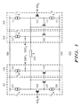
- FIG. 1 shows a transconductance amplifier 100 having a first input circuit 101, a second input circuit 102, a first output circuit 103 and a second output circuit 104, with the first input circuit 101 and the second input circuit 102 being coupled via a resistor 105.
- the first input circuit 101 has a first P-type FET 106 that has its source coupled to a first current source 107, which in turn is coupled to a supply line V DD , and its drain coupled to a second current source 108, which in turn is coupled to a reference line GND, for example ground.
- the gate of the P-type FET 106 acts as the input V in1 for the first input circuit 101.
- the input circuit 101 includes a first N-type FET 109 in which the source is coupled to the reference line GND, the gate is coupled to a point between the first P-type FET drain and the second current source 108, and the drain is coupled to a point between the P-type FET source and the first current source 107 to form a feedback loop.
- the drain of the first N-type FET 109 is additionally coupled to a first interface of the resistor 105.
- the second input circuit 102 is of similar design to the first input circuit 101 having a second P-type FET 110 that has its source coupled to a third current source 111, which in turn is coupled to the supply line V DD , and its drain coupled to a fourth current source 112, which in turn is coupled to the reference line GND, for example ground.
- the gate of the P-type FET 110 acts as the input V in2 for the second input circuit 102.
- the second input circuit 102 includes a second N-type FET 113 in which the source is coupled to the reference line GND, the gate is coupled to a point between the second P-type FET drain and the fourth current source 112, and the drain is coupled to a point between the second P-type FET source and the third current source 111 to form a feedback loop.
- the drain of the second N-type FET 113 is additionally coupled to a second interface of the resistor 105.
- the first output circuit 103 has a third N-type FET 114 that is arranged to form a current mirror with the feedback loop formed by the first N-type FET 109 where the third N-type FET 114 has its source coupled to the reference line GND, its drain couple to a fifth current source 115, which in turn is couple to the supply line V DD , and its gate is coupled to a point between the drain of the first P-type FET 106 and the second current source 108.
- the output I out1 for the first output circuit 103 is formed at a point between the drain of the third N-type FET 114 and the fifth current source 115.
- the second output circuit 104 is of similar design to the first output circuit 103 having a fourth N-type FET 116 that is arranged to form a current mirror with the feedback loop formed by the second N-type FET 113 where the fourth N-type FET 116 has its source coupled to the reference line GND, its drain couple to a sixth current source 117, which in turn is couple to the supply line V DD , and its gate is coupled to a point between the drain of the second P-type FET 110 and the fourth current source 112.
- the output I out2 for the second output circuit 104 is formed at a point between the drain of the fourth N-type FET 116 and the sixth current source 117.
- the voltage across the resistor 105 should be kept equal to the input voltage difference (i.e. V in1 - V in2 ). This is achieved by keeping the drain-source current of the first P-type FET 106 and the second P-type FET 110 constant by means of the feedback loops formed by the first N-type FET 109 and the second N-type FET 113 respectively.
- the feedback loops compensates for current diverted from the first current source 107 and third current source 111 through the resistor 105, thereby ensuring that the drain-source current of the first P-type FET 106 and the second P-type FET 110 is maintained.
- the third N-type FET 114 and fourth N-type FET 116 form current mirrors with the feedback loops their drain-source current will be identical to that for the first N-type FET 109 and second N-type FET 113 respectively, which forms the transconductance amplifier output current I out1 , I out2 .
- the transconductance of the transconductance amplifier 100 is given by 1/R.
- Figure 2 shows a first embodiment of a transconductance amplifier 200 having a fixed transconductance value.
- the transconductance amplifier 200 includes a first input circuit 201, a second input circuit 202, a first output circuit 203 and a second output circuit 204, with the first input circuit 201 and the second input circuit 202 being coupled via a resistor 205.
- the first input circuit 201 has a first P-type FET 206 that has its source coupled to a first current source 207, which in turn is coupled to a supply line V DD , and its drain coupled to a second current source 208, which in turn is coupled to a reference line GND, for example ground.
- the gate of the P-type FET 206 acts as the input V in1 for the first input circuit 201.
- the input circuit 201 includes a first N-type FET 209 that forms a first differential pair with a second N-type FET 210.
- the source of the first N-type FET 209 is coupled to the source of the second N-type FET 210 and to a third current source 211, which in turn is coupled to the reference line GND.
- the gate of the first N-type FET 209 is coupled to a point between the first P-type FET drain and the second current source 208, and the drain is coupled to a point between the P-type FET source and the first current source 207 to form a feedback loop.
- the drain of the first N-type FET 209 is additionally coupled to a first interface of the resistor 205.
- the second input circuit 202 is of similar design to the first input circuit 201 having a second P-type FET 212 that has its source coupled to a fourth current source 213, which in turn is coupled to the supply line V DD , and its drain coupled to a fifth current source 214, which in turn is coupled to the reference line GND, for example ground.
- the gate of the P-type FET 212 acts as the input V in2 for the second input circuit 202.
- the second input circuit 202 includes a third N-type FET 215 that forms a second differential pair with a fourth N-type FET 216.
- the source of the third N-type FET 215 is coupled to the source of the fourth N-type FET 216 and to a sixth current source 217, which in turn is coupled to the reference line GND.
- the gate of the third N-type FET 215 is coupled to a point between the second P-type FET drain and the fifth current source 214, and the drain is coupled to a point between the second P-type FET source and the fourth current source 213 to form a feedback loop.
- the drain of the third N-type FET 215 is additionally coupled to a second interface of the resistor 205.
- the first output circuit includes the second N-type FET 210 that forms a differential pair with the first N-type FET 209.
- the second N-type FET 210 has its source coupled to the source of the first N-type FET 209 and to the third current source 211.
- the gate of the second N-type FET 210 is coupled to a biasing voltage Vg where Vg is selected to accommodate the desired input voltage and required gain.
- the drain of the second N-type FET 210 is coupled to a seventh current source 218, which in turn is coupled to the supply line V DD .
- the output I out1 for the first output circuit 203 is formed at a point between the drain of the second N-type FET 210 and the seventh current source 218.
- the second output circuit 204 includes the fourth N-type FET 216 that forms a differential pair with the third N-type FET 215.
- the fourth N-type FET 216 has its source coupled to the source of the third N-type FET 215 and to the sixth current source 217.
- the gate of the fourth N-type FET 216 is coupled to the biasing voltage V g .
- the drain of the fourth N-type FET 216 is coupled to an eighth current source 219, which in turn is coupled to the supply line V DD .
- the output for the second output circuit 209 is formed at a point between the drain of the fourth N-type FET 216 and the eighth current source 219.
- the voltage across the resistor 205 should be kept equal to the input voltage difference (i.e. V in1 - V in2 ) to obtain a linear voltage to current transfer function.
- V in1 - V in2 the input voltage difference
- the feedback loops compensate for current diverted from the first current source 201 and fourth current source 213 through the resistor 205, thereby ensuring that the drain-source current of the first P-type FET 206 and the second P-type FET 212 is maintained.
- the output current is based upon current difference with respect to the feedback loops. Consequently, due to the use of the differential pairs the first output circuit current flow will be the negative of the current flow in the first feedback loop and the second output circuit current flow will be the negative of the current flow in the second feedback loop, thereby improving transfer linearity and bandwidth compared to the prior art.
- the current generated by the current sources are arranged to have the following multiples:
- the fourth N-type FET 216 i.e. the other half of the second differential pair
- the output current I out2 in the second output circuit 204 is equal to -((V in1 - Vin 2 )/R).
- the output current in the second output circuit 204 is equal to -((V in1 - V in2 )/R) the current flowing into the first N-type FET 209 is reduced by (V in1 - V in2 )/R and this reduced current causes an opposite current flow to flow in the second N-type FET 210 (i.e. the other half of the first differential pair) that is equal to (V in1 - V in2 )/R. Accordingly, the output current I out1 in the first output circuit 203 is equal to (V in1 - V in2 ) /R.
- the transconductance of the transconductance amplifier 200 is given by 1/R.
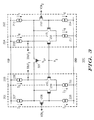
- Figure 3 shows a second embodiment of a transconductance amplifier 300 having a variable transconductance value.
- the transconductance amplifier 300 includes a first input circuit 201, a second input circuit 202, a first output circuit 203 and a second output circuit 204, which are the same as those shown in figure 2 and described above.
- the same reference numerals used in figure 3 as those in figure 1 represent the same features.
- the first input circuit 201 and the second input circuit 202 are coupled via a variable resistor 301 where the variable resistor 301 has a control input V gv .
- the variable resistor is a P-type FET, however, other forms of variable resistor can be used.
- the source and drain of the P-type FET act as the resistors first interface and second interface respectively.
- the gate of the P-type FET acts as the input for the control input V gv , wherein the resistance of the variable resistor is varied via a control voltage applied to the P-type FET gate.
- the transconductance of the transconductance amplifier 300 shown in figure 3 corresponds to the inverse of the resistance of the resistor 301. Accordingly, by varying the value of the resistance, via the control voltage V gv applied to the P-type FET gate, the transconductance of the transconductance amplifier 300 can be varied.
- Figure 4 shows a third embodiment of a transconductance amplifier 400 having a variable transconductance value.
- the transconductance amplifier 400 includes a first input circuit 201, a second input circuit 202, a first output circuit 203 and a second output circuit 204, which are the same as shown in figure 2 and 3 and described above where the same reference numerals used in figure 4 as those in figure 2 and 3 represent the same features.
- the source of a fifth N-type FET 401 is coupled to the source of the first N-type FET 209 and the second N-type FET 210, which form the first differential pair
- the source of a sixth N-type FET 402 is coupled to the source of the third N-type FET 215 and the fourth N-type FET 216, which form the second differential pair.
- the drains of the fifth N-type FET 401 and the sixth N-type FET 402 are coupled to the supply line V DD .
- the gates of the fifth N-type FET 401 and the sixth N-type FET 402 are both coupled to a control voltage V c .
- the first N-type FET 209, the second N-type FET 210 and the fifth N-type FET 401 form a first differential pair and the third N-type FET 215, the fourth N-type FET 216 and the seventh N-type FET 402 form a second differential pair.
- a common mode loop 403 is coupled to the seventh current source 218 and eighth current source 219.
- the common mode loop 403 is an amplifier that corrects the current flow in the seventh current source 218 and the eighth current source 219 if the output common mode voltage moves away from an input reference voltage Vref.
- the transconductance amplifier 400 shown in figure 4 operates in a similar matter to the transconductance amplifier 200 shown in figure 2, however, by changing the control voltage V c applied to the gates of the fifth N-type FET 401 and the sixth N-type FET 402 the amount of current that flows in the fifth N-type FET 401 and the sixth N-type FET 402 correspondingly changes, thereby changing the amount of current that flows in the first N-type FET 209, the second N-type FET 210, the third N-type FET 215 and the fourth N-type FET 216.
- the higher the control voltage V c applied to the gates of the fifth N-type FET 401 and the sixth N-type FET 402 the higher the current flow through the fifth N-type FET 401 and the sixth N-type FET 402 and correspondingly the less current flow through the first N-type FET 209, the second N-type FET 210, the third N-type FET 215 and the fourth N-type FET 216, thereby reducing the transconductance of the transconductance amplifier 400.
- control voltage V c applied to the gates of the fifth N-type FET 401 and the sixth N-type FET 402 is set low then no current will flow through the fifth N-type FET 401 and the sixth N-type FET 402 and the transconductance amplifier 400 will operate in the same manner as that shown and described in figure 2.
- the common mode loop 403 is used to maintain the current flow from the seventh current source 218 equal to the DC current in the second N-type FET 210 and correspondingly the current flow from the eighth current source 219 equal to the DC current in the fourth N-type FET 216.
Landscapes
- Engineering & Computer Science (AREA)
- Power Engineering (AREA)
- Amplifiers (AREA)
- Networks Using Active Elements (AREA)
Abstract
Description
- The present invention relates to a transconductance amplifier.
- Transconductance amplifiers are used for converting an input voltage into an output current.
- Many applications require a transconductance amplifier that has linear transfer characteristics and operates over a wide bandwidth.
- One solution, shown in figure 1, shows a
transconductance amplifier 100 having afirst input circuit 101, asecond input circuit 102, afirst output circuit 103 and asecond output circuit 104, with thefirst input circuit 101 and thesecond input circuit 102 being coupled via aresistor 105. - The
first input circuit 101 has a first P-type FET 106 that has its source coupled to a firstcurrent source 107, which in turn is coupled to a supply line VDD, and its drain coupled to a secondcurrent source 108, which in turn is coupled to a reference line GND, for example ground. The gate of the P-type FET 106 acts as the input Vin1 for thefirst input circuit 101. Additionally, theinput circuit 101 includes a first N-type FET 109 in which the source is coupled to the reference line GND, the gate is coupled to a point between the first P-type FET drain and the secondcurrent source 108, and the drain is coupled to a point between the P-type FET source and the firstcurrent source 107 to form a feedback loop. The drain of the first N-type FET 109 is additionally coupled to a first interface of theresistor 105. - The
second input circuit 102 is of similar design to thefirst input circuit 101 having a second P-type FET 110 that has its source coupled to a thirdcurrent source 111, which in turn is coupled to the supply line VDD, and its drain coupled to a fourthcurrent source 112, which in turn is coupled to the reference line GND, for example ground. The gate of the P-type FET 110 acts as the input Vin2 for thesecond input circuit 102. Additionally, thesecond input circuit 102 includes a second N-type FET 113 in which the source is coupled to the reference line GND, the gate is coupled to a point between the second P-type FET drain and the fourthcurrent source 112, and the drain is coupled to a point between the second P-type FET source and the thirdcurrent source 111 to form a feedback loop. The drain of the second N-type FET 113 is additionally coupled to a second interface of theresistor 105. - The
first output circuit 103 has a third N-type FET 114 that is arranged to form a current mirror with the feedback loop formed by the first N-type FET 109 where the third N-type FET 114 has its source coupled to the reference line GND, its drain couple to a fifthcurrent source 115, which in turn is couple to the supply line VDD, and its gate is coupled to a point between the drain of the first P-type FET 106 and the secondcurrent source 108. The output Iout1 for thefirst output circuit 103 is formed at a point between the drain of the third N-type FET 114 and the fifthcurrent source 115. - The
second output circuit 104 is of similar design to thefirst output circuit 103 having a fourth N-type FET 116 that is arranged to form a current mirror with the feedback loop formed by the second N-type FET 113 where the fourth N-type FET 116 has its source coupled to the reference line GND, its drain couple to a sixthcurrent source 117, which in turn is couple to the supply line VDD, and its gate is coupled to a point between the drain of the second P-type FET 110 and the fourthcurrent source 112. The output Iout2 for thesecond output circuit 104 is formed at a point between the drain of the fourth N-type FET 116 and the sixthcurrent source 117. - In order to obtain a linear voltage to current transfer function the voltage across the
resistor 105 should be kept equal to the input voltage difference (i.e. Vin1 - Vin2). This is achieved by keeping the drain-source current of the first P-type FET 106 and the second P-type FET 110 constant by means of the feedback loops formed by the first N-type FET 109 and the second N-type FET 113 respectively. The feedback loops compensates for current diverted from the firstcurrent source 107 and thirdcurrent source 111 through theresistor 105, thereby ensuring that the drain-source current of the first P-type FET 106 and the second P-type FET 110 is maintained. - As the third N-
type FET 114 and fourth N-type FET 116 form current mirrors with the feedback loops their drain-source current will be identical to that for the first N-type FET 109 and second N-type FET 113 respectively, which forms the transconductance amplifier output current Iout1, Iout2. - By way of illustration, when the input voltage difference is zero (i.e. Vin1 - Vin2 = 0) no current will flow through the
resistor 105 and consequently the current that flows through the first N-type FET 109 and the second N-type FET 113 is identical to the current flow in the output circuits and consequently there will be no output current. - When the input voltage difference is positive (i.e. Vin1 - Vin2 >0) a current (i.e. Vin1 - Vin2 /R) will flow into the
resistor 105 and increase the current in the second N-type FET 113 by the same amount. This current is copied by the second N-type FET/fourth N-type FET current mirror arrangement into the fourth N-type FET 116 to provide an output current in thesecond output circuit 104 that is equal to (Vin1 - Vin2)/R. - Correspondingly, when the output current in the
second output circuit 104 is equal to (Vin1 - Vin2)/R the current flowing into the first N-type FET 109 is reduced by (Vin1 - Vin2)/R and this reduced current is copied into the third N-type FET 114 to provide an output current in thefirst output circuit 103 that is equal to -(Vin1 - Vin2)/R. - As the output current from the
first output circuit 103 equals the negative of thesecond output circuit 104 the transconductance of thetransconductance amplifier 100 is given by 1/R. - However, even though current mirrors are well suited for mirroring fixed currents they are not so suitable for mirroring variable currents. Consequently, the use of a current mirror to generate the transconductance amplifier's output current can limit the linearity of the voltage to current transfer function.
- It is desirable to improve this situation.
- In accordance with an aspect of the present invention there is provided a transconductance amplifier according to
claim 1. - An embodiment of the invention will now be described, by way of example, with reference to the drawings, of which:
- Figure 1 illustrates a prior art transconductance amplifier;
- Figure 2 illustrates a transconductance according to a first embodiment of the present invention;
- Figure 3 illustrates a transconductance according to a second embodiment of the present invention;
- Figure 4 illustrates a transconductance according to a third embodiment of the present invention.
-
- Figure 2 shows a first embodiment of a
transconductance amplifier 200 having a fixed transconductance value. - The
transconductance amplifier 200 includes afirst input circuit 201, asecond input circuit 202, afirst output circuit 203 and asecond output circuit 204, with thefirst input circuit 201 and thesecond input circuit 202 being coupled via aresistor 205. - The
first input circuit 201 has a first P-type FET 206 that has its source coupled to a firstcurrent source 207, which in turn is coupled to a supply line VDD, and its drain coupled to a secondcurrent source 208, which in turn is coupled to a reference line GND, for example ground. The gate of the P-type FET 206 acts as the input Vin1 for thefirst input circuit 201. Additionally, theinput circuit 201 includes a first N-type FET 209 that forms a first differential pair with a second N-type FET 210. The source of the first N-type FET 209 is coupled to the source of the second N-type FET 210 and to a thirdcurrent source 211, which in turn is coupled to the reference line GND. The gate of the first N-type FET 209 is coupled to a point between the first P-type FET drain and the secondcurrent source 208, and the drain is coupled to a point between the P-type FET source and the firstcurrent source 207 to form a feedback loop. The drain of the first N-type FET 209 is additionally coupled to a first interface of theresistor 205. - The
second input circuit 202 is of similar design to thefirst input circuit 201 having a second P-type FET 212 that has its source coupled to a fourthcurrent source 213, which in turn is coupled to the supply line VDD, and its drain coupled to a fifthcurrent source 214, which in turn is coupled to the reference line GND, for example ground. The gate of the P-type FET 212 acts as the input Vin2 for thesecond input circuit 202. Additionally, thesecond input circuit 202 includes a third N-type FET 215 that forms a second differential pair with a fourth N-type FET 216. The source of the third N-type FET 215 is coupled to the source of the fourth N-type FET 216 and to a sixthcurrent source 217, which in turn is coupled to the reference line GND. The gate of the third N-type FET 215 is coupled to a point between the second P-type FET drain and the fifthcurrent source 214, and the drain is coupled to a point between the second P-type FET source and the fourthcurrent source 213 to form a feedback loop. The drain of the third N-type FET 215 is additionally coupled to a second interface of theresistor 205. - The first output circuit includes the second N-type FET 210 that forms a differential pair with the first N-
type FET 209. As stated above, the second N-type FET 210 has its source coupled to the source of the first N-type FET 209 and to the thirdcurrent source 211. The gate of the second N-type FET 210 is coupled to a biasing voltage Vg where Vg is selected to accommodate the desired input voltage and required gain. The drain of the second N-type FET 210 is coupled to a seventhcurrent source 218, which in turn is coupled to the supply line VDD. The output Iout1 for thefirst output circuit 203 is formed at a point between the drain of the second N-type FET 210 and the seventhcurrent source 218. - The
second output circuit 204 includes the fourth N-type FET 216 that forms a differential pair with the third N-type FET 215. As stated above, the fourth N-type FET 216 has its source coupled to the source of the third N-type FET 215 and to the sixthcurrent source 217. The gate of the fourth N-type FET 216 is coupled to the biasing voltage Vg. The drain of the fourth N-type FET 216 is coupled to an eighthcurrent source 219, which in turn is coupled to the supply line VDD. The output for the second output circuit 209is formed at a point between the drain of the fourth N-type FET 216 and the eighthcurrent source 219. - As with the prior art solution, the voltage across the
resistor 205 should be kept equal to the input voltage difference (i.e. Vin1 - Vin2) to obtain a linear voltage to current transfer function. This is achieve by keeping the drain-source current of the first P-type FET 206 and the second P-type FET 212 constant by means of the feedback loops formed by the first N-type FET 209 and the third N-type FET 215 respectively. The feedback loops compensate for current diverted from the firstcurrent source 201 and fourthcurrent source 213 through theresistor 205, thereby ensuring that the drain-source current of the first P-type FET 206 and the second P-type FET 212 is maintained. - However, rather than the output current mirroring the current flowing in the feedback loops, as with the prior art, the output current is based upon current difference with respect to the feedback loops. Consequently, due to the use of the differential pairs the first output circuit current flow will be the negative of the current flow in the first feedback loop and the second output circuit current flow will be the negative of the current flow in the second feedback loop, thereby improving transfer linearity and bandwidth compared to the prior art.
- For the purposes of this embodiment the current generated by the current sources are arranged to have the following multiples:
- Third current source = 2 x Seventh current source ; First current source = Second current source + Seventh current source ; Sixth current source = 2 x Eighth current source ; Fourth current source = Fifth current source + Eighth current source.
- By way of illustration, when the input voltage difference is zero (i.e. Vin1 - Vin2 0) no current will flow through the
resistor 205 and consequently the current that flows through the first N-type FET 209 and the third N-type FET 215 is identical to the current flow in the output circuits and consequently there will be no output current. - When the input voltage difference is positive (i.e. Vin1 - Vin2 >0) a current (i.e. (Vin1 - Vin2)/R) will flow into the
resistor 205 and add to the current in the third N-type FET 215. - To compensate for the increase in current flow in the third N-
type FET 215 an opposite current flow flows in the fourth N-type FET 216 (i.e. the other half of the second differential pair) to provide an output current Iout2 in thesecond output circuit 204 that is equal to -((Vin1 - Vin2)/R). Accordingly, the output current Iout2 in thesecond output circuit 204 is equal to -((Vin1 - Vin2)/R). - Correspondingly, when the output current in the
second output circuit 204 is equal to -((Vin1 - Vin2)/R) the current flowing into the first N-type FET 209 is reduced by (Vin1 - Vin2)/R and this reduced current causes an opposite current flow to flow in the second N-type FET 210 (i.e. the other half of the first differential pair) that is equal to (Vin1 - Vin2)/R. Accordingly, the output current Iout1 in thefirst output circuit 203 is equal to (Vin1 - Vin2) /R. - As the output current from the
first output circuit 203 equals the negative of thesecond output circuit 204 the transconductance of thetransconductance amplifier 200 is given by 1/R. - Figure 3 shows a second embodiment of a
transconductance amplifier 300 having a variable transconductance value. - The
transconductance amplifier 300 includes afirst input circuit 201, asecond input circuit 202, afirst output circuit 203 and asecond output circuit 204, which are the same as those shown in figure 2 and described above. The same reference numerals used in figure 3 as those in figure 1 represent the same features. - The
first input circuit 201 and thesecond input circuit 202 are coupled via a variable resistor 301 where the variable resistor 301 has a control input Vgv. For the purpose of this embodiment the variable resistor is a P-type FET, however, other forms of variable resistor can be used. The source and drain of the P-type FET act as the resistors first interface and second interface respectively. The gate of the P-type FET acts as the input for the control input Vgv, wherein the resistance of the variable resistor is varied via a control voltage applied to the P-type FET gate. - As described above, the transconductance of the
transconductance amplifier 300 shown in figure 3 corresponds to the inverse of the resistance of the resistor 301. Accordingly, by varying the value of the resistance, via the control voltage Vgv applied to the P-type FET gate, the transconductance of thetransconductance amplifier 300 can be varied. - Figure 4 shows a third embodiment of a
transconductance amplifier 400 having a variable transconductance value. - As with figure 2 and figure 3 the
transconductance amplifier 400 includes afirst input circuit 201, asecond input circuit 202, afirst output circuit 203 and asecond output circuit 204, which are the same as shown in figure 2 and 3 and described above where the same reference numerals used in figure 4 as those in figure 2 and 3 represent the same features. - As shown in figure 4 the source of a fifth N-
type FET 401 is coupled to the source of the first N-type FET 209 and the second N-type FET 210, which form the first differential pair, and the source of a sixth N-type FET 402 is coupled to the source of the third N-type FET 215 and the fourth N-type FET 216, which form the second differential pair. The drains of the fifth N-type FET 401 and the sixth N-type FET 402 are coupled to the supply line VDD. The gates of the fifth N-type FET 401 and the sixth N-type FET 402 are both coupled to a control voltage Vc. - Accordingly, the first N-
type FET 209, the second N-type FET 210 and the fifth N-type FET 401 form a first differential pair and the third N-type FET 215, the fourth N-type FET 216 and the seventh N-type FET 402 form a second differential pair. - Additionally, a
common mode loop 403 is coupled to the seventhcurrent source 218 and eighthcurrent source 219. In this embodiment thecommon mode loop 403 is an amplifier that corrects the current flow in the seventhcurrent source 218 and the eighthcurrent source 219 if the output common mode voltage moves away from an input reference voltage Vref. - The
transconductance amplifier 400 shown in figure 4 operates in a similar matter to thetransconductance amplifier 200 shown in figure 2, however, by changing the control voltage Vc applied to the gates of the fifth N-type FET 401 and the sixth N-type FET 402 the amount of current that flows in the fifth N-type FET 401 and the sixth N-type FET 402 correspondingly changes, thereby changing the amount of current that flows in the first N-type FET 209, the second N-type FET 210, the third N-type FET 215 and the fourth N-type FET 216. - Accordingly, the higher the control voltage Vc applied to the gates of the fifth N-
type FET 401 and the sixth N-type FET 402 the higher the current flow through the fifth N-type FET 401 and the sixth N-type FET 402 and correspondingly the less current flow through the first N-type FET 209, the second N-type FET 210, the third N-type FET 215 and the fourth N-type FET 216, thereby reducing the transconductance of thetransconductance amplifier 400. - If the control voltage Vc applied to the gates of the fifth N-
type FET 401 and the sixth N-type FET 402 is set low then no current will flow through the fifth N-type FET 401 and the sixth N-type FET 402 and thetransconductance amplifier 400 will operate in the same manner as that shown and described in figure 2. - A consequence of reducing the transconductance by increasing the control voltage to the gates of the fifth N-
type FET 401 and the sixth N-type FET 402 results in a reduction in DC current flow into the second N-type FET 210 and the fourth N-type FET 216. Accordingly, thecommon mode loop 403 is used to maintain the current flow from the seventhcurrent source 218 equal to the DC current in the second N-type FET 210 and correspondingly the current flow from the eighthcurrent source 219 equal to the DC current in the fourth N-type FET 216.
Claims (6)
- A transconductance amplifier comprising a first input circuit having a first feedback loop; a second input circuit having a second feedback loop; a resistor having a first interface connected to the first input circuit and a second interface connected to the second input circuit; a first differential pair having a first transistor arranged to control current flow in the first feedback loop to maintain a voltage at the first interface of the resistor at substantially a constant voltage relative to an input voltage applied to the first input circuit and a second transistor arranged to control current flow for a first output; and a second differential pair having a third transistor arranged to control current flow in the second feedback loop to maintain a voltage at the second interface of the resistor at substantially a constant voltage relative to an input voltage applied to the second input circuit and a fourth transistor arranged to control current flow for a second output.
- A transconductance amplifier according to claim 1, wherein the transconductance is the inverse of the resistance of the resistor.
- A transconductance amplifier according to claim 1 or 2, wherein the resistor is a fixed resistor.
- A transconductance amplifier according to claim 1 or 2, wherein the resistor is a variable resistor to allow the transconductance of the transconductance amplifier to be varied.
- A transconductance amplifier according to any preceding claim, wherein the first differential pair further comprises a fifth transistor and the second differential pair further comprises a sixth transistor, wherein the fifth transistor and sixth transistor are arranged to be coupled to a control signal for varying the current flow for the first output and the current flow for the second output respectively, thereby allowing the transconductance to be varied.
- A transconductance amplifier according to claim 5, further comprising a common-mode loop arranged to maintain an output current substantially equal to zero when the voltage difference between the input voltage applied to the first input circuit and the input voltage applied to the second input circuit is substantially zero.
Priority Applications (4)
| Application Number | Priority Date | Filing Date | Title |
|---|---|---|---|
| DE60314754T DE60314754T2 (en) | 2003-10-27 | 2003-10-27 | transconductance amplifier |
| AT03292679T ATE366482T1 (en) | 2003-10-27 | 2003-10-27 | TRANSCONDUCTANCE AMPLIFIER |
| EP03292679A EP1528670B1 (en) | 2003-10-27 | 2003-10-27 | Transconductance amplifier |
| US10/973,728 US7183848B2 (en) | 2003-10-27 | 2004-10-26 | Transconductance amplifier |
Applications Claiming Priority (1)
| Application Number | Priority Date | Filing Date | Title |
|---|---|---|---|
| EP03292679A EP1528670B1 (en) | 2003-10-27 | 2003-10-27 | Transconductance amplifier |
Publications (2)
| Publication Number | Publication Date |
|---|---|
| EP1528670A1 true EP1528670A1 (en) | 2005-05-04 |
| EP1528670B1 EP1528670B1 (en) | 2007-07-04 |
Family
ID=34400583
Family Applications (1)
| Application Number | Title | Priority Date | Filing Date |
|---|---|---|---|
| EP03292679A Expired - Lifetime EP1528670B1 (en) | 2003-10-27 | 2003-10-27 | Transconductance amplifier |
Country Status (4)
| Country | Link |
|---|---|
| US (1) | US7183848B2 (en) |
| EP (1) | EP1528670B1 (en) |
| AT (1) | ATE366482T1 (en) |
| DE (1) | DE60314754T2 (en) |
Families Citing this family (2)
| Publication number | Priority date | Publication date | Assignee | Title |
|---|---|---|---|---|
| JP5315981B2 (en) * | 2008-12-24 | 2013-10-16 | 富士通セミコンダクター株式会社 | CURRENT GENERATION CIRCUIT, CURRENT GENERATION METHOD, AND ELECTRONIC DEVICE |
| CN108900169A (en) * | 2018-09-18 | 2018-11-27 | 上海新进半导体制造有限公司 | A kind of Hall amplifier |
Citations (1)
| Publication number | Priority date | Publication date | Assignee | Title |
|---|---|---|---|---|
| US20030052731A1 (en) * | 2000-08-30 | 2003-03-20 | Nec Corporation | Linear voltage subtractor/adder circuit and MOS differential amplifier circuit therefor |
Family Cites Families (1)
| Publication number | Priority date | Publication date | Assignee | Title |
|---|---|---|---|---|
| US5307024A (en) * | 1992-07-27 | 1994-04-26 | Tektronix, Inc. | Linearized level-shifting amplifier |
-
2003
- 2003-10-27 DE DE60314754T patent/DE60314754T2/en not_active Expired - Lifetime
- 2003-10-27 EP EP03292679A patent/EP1528670B1/en not_active Expired - Lifetime
- 2003-10-27 AT AT03292679T patent/ATE366482T1/en not_active IP Right Cessation
-
2004
- 2004-10-26 US US10/973,728 patent/US7183848B2/en not_active Expired - Lifetime
Patent Citations (1)
| Publication number | Priority date | Publication date | Assignee | Title |
|---|---|---|---|---|
| US20030052731A1 (en) * | 2000-08-30 | 2003-03-20 | Nec Corporation | Linear voltage subtractor/adder circuit and MOS differential amplifier circuit therefor |
Non-Patent Citations (2)
| Title |
|---|
| ISMAIL A M ET AL: "NOVEL CMOS LINEARISED BALANCED OUTPUT TRANSCONDUCTANCE AMPLIFIER BASED ON DIFFERENTIAL PAIRS EIN NEUER LINEARISIERTER DIFFERENTIALVERSTAERKER FUER CMOS TECHNOLOGIE MIT SYMMETRISCHEN AUSGANGSUEBERTRAGUNGSLEITWERT", FREQUENZ, SCHIELE UND SCHON GMBH. BERLIN, DE, VOL. 53, NR. 7/8, PAGE(S) 170-174, ISSN: 0016-1136, XP000920024 * |
| TOWERS T D: "BALANCED TRANSISTOR D.C. AMPLIFIERS HOW MODERN DIFFUSED SILICON TRANSISTORS AND F.E.TS ARE USED TO AMPLIFY D.C. LOW-LEVEL CURRENTS AND VOLTAGES", WIRELESS WORLD, IPC BUSINESS PRESS LTD. HAYWARDS HEATH, GB, VOL. 74, NR. 1394, PAGE(S) 269-274, XP001127064 * |
Also Published As
| Publication number | Publication date |
|---|---|
| EP1528670B1 (en) | 2007-07-04 |
| US20050088234A1 (en) | 2005-04-28 |
| DE60314754T2 (en) | 2007-12-06 |
| US7183848B2 (en) | 2007-02-27 |
| DE60314754D1 (en) | 2007-08-16 |
| ATE366482T1 (en) | 2007-07-15 |
Similar Documents
| Publication | Publication Date | Title |
|---|---|---|
| US7911244B2 (en) | Differential drive circuit and communication device | |
| CN101447785B (en) | Differential drive circuit and communication device | |
| US20120001605A1 (en) | Differential amplifier circuit and series regulator | |
| US7652535B2 (en) | Continuous time common mode feedback circuit, system, and method | |
| JP2008288900A (en) | Differential amplifier | |
| US7446607B2 (en) | Regulated cascode circuit, an amplifier including the same, and method of regulating a cascode circuit | |
| US8587287B2 (en) | High-bandwidth linear current mirror | |
| US7253685B2 (en) | Class AB amplifier having adjustable quiescent current and output current | |
| US6756841B2 (en) | Variable offset amplifier circuits and their applications | |
| US20090184752A1 (en) | Bias circuit | |
| CN108964617A (en) | Operational amplifier circuit | |
| US6653894B2 (en) | Integrated current mirror in output stage of operational amplifier | |
| US11742812B2 (en) | Output pole-compensated operational amplifier | |
| US7183848B2 (en) | Transconductance amplifier | |
| EP1626496B1 (en) | Differential gain stage for low voltage supply | |
| US6366169B1 (en) | Fast rail-to-rail class AB output stage having stable output bias current and linear performance | |
| US6803819B2 (en) | Variable gain amplifier having improved gain slope characteristic and linearity | |
| CN105897183A (en) | Circuit and amplifier with deterministic noise cancellation | |
| EP1017164A2 (en) | Current mirror with a constant current for a wide range of output load impedance | |
| US12601767B2 (en) | Current sense amplifier | |
| US20220069790A1 (en) | Operational Amplifier | |
| WO2021124450A1 (en) | Differential amplification circuit, reception circuit and semiconductor integrated circuit | |
| US20260100685A1 (en) | Current mirror operational transconductance amplifier | |
| JP2021164055A (en) | Fully differential amplifier | |
| US20260098879A1 (en) | Current sense amplifier |
Legal Events
| Date | Code | Title | Description |
|---|---|---|---|
| PUAI | Public reference made under article 153(3) epc to a published international application that has entered the european phase |
Free format text: ORIGINAL CODE: 0009012 |
|
| AK | Designated contracting states |
Kind code of ref document: A1 Designated state(s): AT BE BG CH CY CZ DE DK EE ES FI FR GB GR HU IE IT LI LU MC NL PT RO SE SI SK TR |
|
| AX | Request for extension of the european patent |
Extension state: AL LT LV MK |
|
| 17P | Request for examination filed |
Effective date: 20051104 |
|
| AKX | Designation fees paid |
Designated state(s): AT BE BG CH CY CZ DE DK EE ES FI FR GB GR HU IE IT LI LU MC NL PT RO SE SI SK TR |
|
| GRAP | Despatch of communication of intention to grant a patent |
Free format text: ORIGINAL CODE: EPIDOSNIGR1 |
|
| 17Q | First examination report despatched |
Effective date: 20060213 |
|
| GRAS | Grant fee paid |
Free format text: ORIGINAL CODE: EPIDOSNIGR3 |
|
| GRAA | (expected) grant |
Free format text: ORIGINAL CODE: 0009210 |
|
| AK | Designated contracting states |
Kind code of ref document: B1 Designated state(s): AT BE BG CH CY CZ DE DK EE ES FI FR GB GR HU IE IT LI LU MC NL PT RO SE SI SK TR |
|
| REG | Reference to a national code |
Ref country code: GB Ref legal event code: FG4D |
|
| REG | Reference to a national code |
Ref country code: CH Ref legal event code: EP |
|
| REG | Reference to a national code |
Ref country code: IE Ref legal event code: FG4D |
|
| REF | Corresponds to: |
Ref document number: 60314754 Country of ref document: DE Date of ref document: 20070816 Kind code of ref document: P |
|
| ET | Fr: translation filed | ||
| NLV1 | Nl: lapsed or annulled due to failure to fulfill the requirements of art. 29p and 29m of the patents act | ||
| REG | Reference to a national code |
Ref country code: CH Ref legal event code: PL |
|
| PG25 | Lapsed in a contracting state [announced via postgrant information from national office to epo] |
Ref country code: PT Free format text: LAPSE BECAUSE OF FAILURE TO SUBMIT A TRANSLATION OF THE DESCRIPTION OR TO PAY THE FEE WITHIN THE PRESCRIBED TIME-LIMIT Effective date: 20071204 Ref country code: BG Free format text: LAPSE BECAUSE OF FAILURE TO SUBMIT A TRANSLATION OF THE DESCRIPTION OR TO PAY THE FEE WITHIN THE PRESCRIBED TIME-LIMIT Effective date: 20071004 Ref country code: SI Free format text: LAPSE BECAUSE OF FAILURE TO SUBMIT A TRANSLATION OF THE DESCRIPTION OR TO PAY THE FEE WITHIN THE PRESCRIBED TIME-LIMIT Effective date: 20070704 Ref country code: ES Free format text: LAPSE BECAUSE OF FAILURE TO SUBMIT A TRANSLATION OF THE DESCRIPTION OR TO PAY THE FEE WITHIN THE PRESCRIBED TIME-LIMIT Effective date: 20071015 Ref country code: FI Free format text: LAPSE BECAUSE OF FAILURE TO SUBMIT A TRANSLATION OF THE DESCRIPTION OR TO PAY THE FEE WITHIN THE PRESCRIBED TIME-LIMIT Effective date: 20070704 Ref country code: NL Free format text: LAPSE BECAUSE OF FAILURE TO SUBMIT A TRANSLATION OF THE DESCRIPTION OR TO PAY THE FEE WITHIN THE PRESCRIBED TIME-LIMIT Effective date: 20070704 |
|
| PG25 | Lapsed in a contracting state [announced via postgrant information from national office to epo] |
Ref country code: LI Free format text: LAPSE BECAUSE OF FAILURE TO SUBMIT A TRANSLATION OF THE DESCRIPTION OR TO PAY THE FEE WITHIN THE PRESCRIBED TIME-LIMIT Effective date: 20070704 Ref country code: AT Free format text: LAPSE BECAUSE OF FAILURE TO SUBMIT A TRANSLATION OF THE DESCRIPTION OR TO PAY THE FEE WITHIN THE PRESCRIBED TIME-LIMIT Effective date: 20070704 Ref country code: CH Free format text: LAPSE BECAUSE OF FAILURE TO SUBMIT A TRANSLATION OF THE DESCRIPTION OR TO PAY THE FEE WITHIN THE PRESCRIBED TIME-LIMIT Effective date: 20070704 |
|
| PG25 | Lapsed in a contracting state [announced via postgrant information from national office to epo] |
Ref country code: BE Free format text: LAPSE BECAUSE OF FAILURE TO SUBMIT A TRANSLATION OF THE DESCRIPTION OR TO PAY THE FEE WITHIN THE PRESCRIBED TIME-LIMIT Effective date: 20070704 |
|
| PG25 | Lapsed in a contracting state [announced via postgrant information from national office to epo] |
Ref country code: GR Free format text: LAPSE BECAUSE OF FAILURE TO SUBMIT A TRANSLATION OF THE DESCRIPTION OR TO PAY THE FEE WITHIN THE PRESCRIBED TIME-LIMIT Effective date: 20071005 Ref country code: DK Free format text: LAPSE BECAUSE OF FAILURE TO SUBMIT A TRANSLATION OF THE DESCRIPTION OR TO PAY THE FEE WITHIN THE PRESCRIBED TIME-LIMIT Effective date: 20070704 |
|
| PLBE | No opposition filed within time limit |
Free format text: ORIGINAL CODE: 0009261 |
|
| STAA | Information on the status of an ep patent application or granted ep patent |
Free format text: STATUS: NO OPPOSITION FILED WITHIN TIME LIMIT |
|
| PG25 | Lapsed in a contracting state [announced via postgrant information from national office to epo] |
Ref country code: MC Free format text: LAPSE BECAUSE OF NON-PAYMENT OF DUE FEES Effective date: 20071031 Ref country code: SK Free format text: LAPSE BECAUSE OF FAILURE TO SUBMIT A TRANSLATION OF THE DESCRIPTION OR TO PAY THE FEE WITHIN THE PRESCRIBED TIME-LIMIT Effective date: 20070704 Ref country code: CZ Free format text: LAPSE BECAUSE OF FAILURE TO SUBMIT A TRANSLATION OF THE DESCRIPTION OR TO PAY THE FEE WITHIN THE PRESCRIBED TIME-LIMIT Effective date: 20070704 |
|
| 26N | No opposition filed |
Effective date: 20080407 |
|
| PG25 | Lapsed in a contracting state [announced via postgrant information from national office to epo] |
Ref country code: SE Free format text: LAPSE BECAUSE OF FAILURE TO SUBMIT A TRANSLATION OF THE DESCRIPTION OR TO PAY THE FEE WITHIN THE PRESCRIBED TIME-LIMIT Effective date: 20071004 Ref country code: RO Free format text: LAPSE BECAUSE OF FAILURE TO SUBMIT A TRANSLATION OF THE DESCRIPTION OR TO PAY THE FEE WITHIN THE PRESCRIBED TIME-LIMIT Effective date: 20070704 |
|
| PG25 | Lapsed in a contracting state [announced via postgrant information from national office to epo] |
Ref country code: IE Free format text: LAPSE BECAUSE OF NON-PAYMENT OF DUE FEES Effective date: 20071030 |
|
| PG25 | Lapsed in a contracting state [announced via postgrant information from national office to epo] |
Ref country code: EE Free format text: LAPSE BECAUSE OF FAILURE TO SUBMIT A TRANSLATION OF THE DESCRIPTION OR TO PAY THE FEE WITHIN THE PRESCRIBED TIME-LIMIT Effective date: 20070704 |
|
| PG25 | Lapsed in a contracting state [announced via postgrant information from national office to epo] |
Ref country code: CY Free format text: LAPSE BECAUSE OF FAILURE TO SUBMIT A TRANSLATION OF THE DESCRIPTION OR TO PAY THE FEE WITHIN THE PRESCRIBED TIME-LIMIT Effective date: 20070704 |
|
| PG25 | Lapsed in a contracting state [announced via postgrant information from national office to epo] |
Ref country code: LU Free format text: LAPSE BECAUSE OF NON-PAYMENT OF DUE FEES Effective date: 20071027 |
|
| PG25 | Lapsed in a contracting state [announced via postgrant information from national office to epo] |
Ref country code: HU Free format text: LAPSE BECAUSE OF FAILURE TO SUBMIT A TRANSLATION OF THE DESCRIPTION OR TO PAY THE FEE WITHIN THE PRESCRIBED TIME-LIMIT Effective date: 20080105 Ref country code: TR Free format text: LAPSE BECAUSE OF FAILURE TO SUBMIT A TRANSLATION OF THE DESCRIPTION OR TO PAY THE FEE WITHIN THE PRESCRIBED TIME-LIMIT Effective date: 20070704 |
|
| PG25 | Lapsed in a contracting state [announced via postgrant information from national office to epo] |
Ref country code: IT Free format text: LAPSE BECAUSE OF NON-PAYMENT OF DUE FEES Effective date: 20071031 |
|
| PGFP | Annual fee paid to national office [announced via postgrant information from national office to epo] |
Ref country code: FR Payment date: 20131017 Year of fee payment: 11 Ref country code: GB Payment date: 20131028 Year of fee payment: 11 |
|
| GBPC | Gb: european patent ceased through non-payment of renewal fee |
Effective date: 20141027 |
|
| PG25 | Lapsed in a contracting state [announced via postgrant information from national office to epo] |
Ref country code: GB Free format text: LAPSE BECAUSE OF NON-PAYMENT OF DUE FEES Effective date: 20141027 |
|
| REG | Reference to a national code |
Ref country code: FR Ref legal event code: ST Effective date: 20150630 |
|
| PG25 | Lapsed in a contracting state [announced via postgrant information from national office to epo] |
Ref country code: FR Free format text: LAPSE BECAUSE OF NON-PAYMENT OF DUE FEES Effective date: 20141031 |
|
| REG | Reference to a national code |
Ref country code: DE Ref legal event code: R082 Ref document number: 60314754 Country of ref document: DE Representative=s name: SCHUMACHER & WILLSAU PATENTANWALTSGESELLSCHAFT, DE Ref country code: DE Ref legal event code: R081 Ref document number: 60314754 Country of ref document: DE Owner name: NXP USA, INC. (N.D.GES.D.STAATES DELAWARE), AU, US Free format text: FORMER OWNER: FREESCALE SEMICONDUCTOR, INC., AUSTIN, TEX., US |
|
| PGFP | Annual fee paid to national office [announced via postgrant information from national office to epo] |
Ref country code: DE Payment date: 20200917 Year of fee payment: 18 |
|
| REG | Reference to a national code |
Ref country code: DE Ref legal event code: R119 Ref document number: 60314754 Country of ref document: DE |
|
| PG25 | Lapsed in a contracting state [announced via postgrant information from national office to epo] |
Ref country code: DE Free format text: LAPSE BECAUSE OF NON-PAYMENT OF DUE FEES Effective date: 20220503 |