EP1528661A1 - Circuit de commande d'un transistor MOS pour redresseur synchrone - Google Patents
Circuit de commande d'un transistor MOS pour redresseur synchrone Download PDFInfo
- Publication number
- EP1528661A1 EP1528661A1 EP04105379A EP04105379A EP1528661A1 EP 1528661 A1 EP1528661 A1 EP 1528661A1 EP 04105379 A EP04105379 A EP 04105379A EP 04105379 A EP04105379 A EP 04105379A EP 1528661 A1 EP1528661 A1 EP 1528661A1
- Authority
- EP
- European Patent Office
- Prior art keywords
- voltage
- switch
- circuit
- terminals
- transistor
- Prior art date
- Legal status (The legal status is an assumption and is not a legal conclusion. Google has not performed a legal analysis and makes no representation as to the accuracy of the status listed.)
- Granted
Links
Images

Classifications
-
- H—ELECTRICITY
- H02—GENERATION; CONVERSION OR DISTRIBUTION OF ELECTRIC POWER
- H02M—APPARATUS FOR CONVERSION BETWEEN AC AND AC, BETWEEN AC AND DC, OR BETWEEN DC AND DC, AND FOR USE WITH MAINS OR SIMILAR POWER SUPPLY SYSTEMS; CONVERSION OF DC OR AC INPUT POWER INTO SURGE OUTPUT POWER; CONTROL OR REGULATION THEREOF
- H02M7/00—Conversion of AC power input into DC power output; Conversion of DC power input into AC power output
- H02M7/02—Conversion of AC power input into DC power output without possibility of reversal
- H02M7/04—Conversion of AC power input into DC power output without possibility of reversal by static converters
- H02M7/12—Conversion of AC power input into DC power output without possibility of reversal by static converters using discharge tubes with control electrode or semiconductor devices with control electrode
- H02M7/21—Conversion of AC power input into DC power output without possibility of reversal by static converters using discharge tubes with control electrode or semiconductor devices with control electrode using devices of a triode or transistor type requiring continuous application of a control signal
- H02M7/217—Conversion of AC power input into DC power output without possibility of reversal by static converters using discharge tubes with control electrode or semiconductor devices with control electrode using devices of a triode or transistor type requiring continuous application of a control signal using semiconductor devices only
-
- H—ELECTRICITY
- H02—GENERATION; CONVERSION OR DISTRIBUTION OF ELECTRIC POWER
- H02M—APPARATUS FOR CONVERSION BETWEEN AC AND AC, BETWEEN AC AND DC, OR BETWEEN DC AND DC, AND FOR USE WITH MAINS OR SIMILAR POWER SUPPLY SYSTEMS; CONVERSION OF DC OR AC INPUT POWER INTO SURGE OUTPUT POWER; CONTROL OR REGULATION THEREOF
- H02M1/00—Details of apparatus for conversion
- H02M1/08—Circuits specially adapted for the generation of control voltages for semiconductor devices incorporated in static converters
- H02M1/083—Circuits specially adapted for the generation of control voltages for semiconductor devices incorporated in static converters for the ignition at the zero crossing of the voltage or the current
Definitions
- the present invention relates to rectifying elements an alternating voltage.
- the invention relates more particularly performing a turnaround function (diode) by means of a MOS transistor.
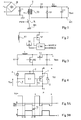
- FIG. 1 represents, very schematically, a first circuit example using rectifying elements of the type to which the present invention can apply.
- a converter is essentially constituted of a transformer T of which a primary winding T1 receives a DC voltage supplied by a capacitor C1 connected in output of a diode bridge B powered by an alternating voltage.
- the winding T1 is connected by a switch K to the mass.
- the switch K is controlled in width modulation impulse by a PWM signal (high frequency compared to alternative power supply) established to regulate a voltage continues Vout supplied by the converter.
- This tension Vout is provided on the secondary side T2 across a capacitor C2 storing energy transferred from primary T1 to secondary T2 of the transformer during periods when the switch K is closed.
- a first end of the secondary winding T2 is connected, by a diode D1 in series with an inductance L1, to a first electrode of the capacitor C2 defining a terminal positive output, while its other end is connected directly to the other electrode of capacitor C2 defining the mass M2 on the voltage side Vout.
- a freewheel diode D2 connects the midpoint of the series association between diode D1 and the inductance L1 to the ground M2, the anode of the diode being mass. The operation of such a converter is known.
- the recovery elements here consist of diodes D1 and D2 which have the drawback of presenting a voltage threshold of between 0.3 and 1.5 volts, detrimental to the converter efficiency, especially in applications low tension.
- Figure 2 illustrates partially and schematically, a modification applied to a PWM converter the FIG. 1 in order to reduce the threshold voltage of the elements of recovery.
- Figure 2 only a part of secondary school has been represented, the rest being similar to Figure 1.
- N1 and N2 To decrease the threshold voltage of the diodes D1 and D2, we replace these by two MOS transistors N channel N1 and N2 that we adequately controlled by a particular CTRL circuit.
- the N1 transistor replacing the diode D1 must however be placed on the branch of converter mass, the transistor N2 can be placed in the same way as diode D2 in FIG.
- CTRL command also receives a supply voltage SUPPLY as well as a synchronization signal SYNCH with respect to the cutting of the DC voltage operated on the primary side, in order to synchronize the respective openings and closures of the transistors N1 and N2 with the openings and closures of the switch K (not shown in FIG. 2).
- a disadvantage of the synchronous rectifying circuit of Figure 2 is that transistors N1 and N2 can not have autonomous operation. They need a signal from synchronization from the primary as well as a voltage Power.
- Another disadvantage is the presence of a transistor MOS on the mass line and not on the high side line secondary.
- Figure 3 illustrates another example of a converter voltage to which the present invention applies. It's about of a DC-DC converter whose role is to raise a output voltage Vout with respect to the level of a voltage V1 input provided, for example, by a battery.
- the electrode positive of the V1 battery is connected to a first end of an inductance L whose other end is connected, by a first MOS transistor N1, at a first electrode of a output capacitor C at the terminals of which is taken the output voltage Vout.
- the midpoint of the series association of inductance L and transistor N1 is also connected, by a transistor N2, at the mass defined by the electrode negative of the battery V1 to which is connected the second capacitor C electrode.
- the control of N1 and N2 transistors is particularly delicate since it requires a level shifter for to control the transistor N1 which has no reference to the mass.
- the present invention aims to propose a circuit of autonomous control of a MOS transistor providing a function of recovery.
- the invention also aims to propose a circuit of autonomous recovery, that is to say, two terminals, including a MOS transistor and its control circuit.
- said predetermined duration is chosen according to the variations expected maximum of the duty cycle.
- a capacitor and a diode are connected in series between the switch terminals to provide a supply voltage to the control circuit, the capacitor being charged when the switch is open.
- a first delay element brings a minimum delay to a opening instruction of the switch following its closure.
- a second delay element brings a delay to the closure of the switch in relation to the inversion of the voltage at its terminals.
- an output amplifier providing the control signal of the switch is controlled by detection means of a reversal of the direction of the tension, to cause the opening of the switch in case of accidental voltage reversal.
- the switch is a MOS transistor.
- a diode in parallel on the switch is used for starting.
- the invention also provides a circuit for low voltage threshold recovery including a switch in parallel with a diode preferably consisting of its diode parasite, and a control circuit associated with a circuit supplying power directly to the terminals of the controlled transistor while it is closed.
- the rectifying circuit has only two terminals of external connection.
- a feature of the present invention is to control a MOS transistor, including the drain and the source define two end terminals of the rectification circuit, by synchronizing his conduction periods exclusively in function of the voltage present at its terminals (between drain and source).
- control circuit is autonomous, that is to say, it takes the energy necessary for its operation at both terminals of the MOS transistor.
- the invention thus achieves a diode function at means of an autonomous circuit having exclusively two terminals to connect to the rest of the application.
- FIG. 4 shows, schematically and under block shape, a MOS transistor rectifying circuit according to the invention.
- This circuit essentially comprises a transistor N-channel MOS 1 whose source defines the anode A of the rectifying circuit and whose drain defines the cathode K.
- a diode 2 is connected in parallel on the transistor 1 with its anode mixed with the source of transistor 1.
- the diode 2 may be constituted by the diode parasite of transistor 1.
- the gate of transistor 1 receives a control voltage Vc supplied by a circuit 3 (CT) which sets the conduction periods of transistor 1 as a function of the voltage detected at its terminals.
- CT circuit 3
- circuit 3 includes two terminals respectively connected to the electrodes K and A.
- the circuit 3 is also powered independently by a voltage Vcc extracted directly from the voltage between the terminals K and A.
- the circuit power supply consists of a diode 4 whose anode is connected to the cathode K of the circuit and whose cathode is connected by a storage capacitor 5 to the anode A.
- voltage Vcc to the circuit 3 is taken from the terminals of capacitor 5.
- alternations are used during which transistor 1 is blocked because the voltage Vd between its K and A terminals is positive (with the conventions taken in the figures) to charge the capacitor 5, the diode 4 being during these periods polarized live.
- the transistor 1 is passed through circuit 3 and diode 4 prevents the capacitor 5 to discharge otherwise than by feeding the circuit 3.
- the invention fulfills a function of rectification in the case where the voltage present between the terminals K and A is a voltage that changes direction, that is, comes from from an alternative source. More particularly, the invention applies in the case where the voltage Vd is of the switching type at relatively high frequency (several tens of kilohertz) so as not to require a capacitor 5 of size too important, as it must maintain a sufficient during the periods when the transistor 1 leads.
- the voltage Vcc needed for operation of circuit 3 could be provided by other means, including for the case where adequate voltage is available in the rest of the circuit.
- getting the voltage Vcc directly by the voltage across the circuit of the invention is preferable to the extent that it allows to obtain a fully autonomous circuit and without reference problem of voltage.
- Figures 5A and 5B respectively illustrate, under form of timing diagrams, an example of a voltage step Vd at terminals of transistor 1 and the corresponding control voltage Vc provided by circuit 3.
- transistor 1 is blocked regardless of the voltage Vd (circuit 3 is not powered and can not the command). Possible conduction during periods when the potential of the terminal A is greater than the potential of the K terminal (negative Vd voltage with the conventions taken at figures) is then ensured by the diode 2 then polarized in direct. Some alternations of the voltage Vd can be necessary to sufficiently charge capacitor 5 and allow the system to boot.
- FIGS 5A and 5B illustrate an example in regime established and, for simplicity, assume a voltage Vd rectangular (for example, from a switching power supply). Everything that will be discussed later also applies in the case of a sinusoidal voltage Vd or the like, provided that it is alternative.
- Vd rectangular for example, from a switching power supply
- the inverse negative voltage in the orientation of the figure
- a first threshold TH1 corresponding to the threshold voltage (of the order of 0.7 volts) of the diode 2.
- Circuit 3 is designed to detect the appearance of this negative voltage and to cause the transistor 1 to close at a time t2 which follows the time t1 with a predetermined duration.
- transistor 1 is turned on, which reduces the voltage drop directly to the voltage of threshold TH2 of this transistor.
- this voltage drop is, at worst, less than 0.2 and can even be reduced to about 50 mV. It is related to the resistance of the MOS transistor to the passing state (RdsON) and therefore depends on the current set by the application. It also depends on the size of the transistor and the avalanche voltage of the technology.
- transistor 1 The opening of transistor 1 must intervene at a moment t3 which precedes a moment (in principle unknown) t4 of change of alternation (transition to the new alternation positive).
- the circuit 3 determines a closing time (t3-t2) compared to the previous period of the voltage Vd.
- the opening of transistor 1 in advance with respect to the appearance of positive alternation is essential for avoid conduction of the system during this alternation positive, which would cancel the desired recovery effect.
- the dead time difference between instants t1 and t2 may be the case should be deleted if the application allows for conduction from the beginning of the negative alternation.
- Figure 6 shows the diagram of an example of embodiment of a circuit 3 according to the invention implementing these functions.
- the transistor 1 we find the transistor 1 to be controlled as well as the diode 2 in parallel.
- the means of Supply of the supply voltage Vcc have not been represented in figure 6. These are, for example, made up of the diode 4 and the capacitor 5 as in FIG.
- FIGS 7A to 7H will be described together with Figure 6 which they explain the operation by chronograms representing examples of gaits in points characteristics of the circuit.
- the detection of the direction of the voltage Vd is carried out at means of a resistive divider bridge R1-R2 connected to terminals K and A and whose midpoint is connected to the input of an inverter 10.
- Inverter 10 serves to digitally shape the signal of detection.
- the voltage V10 (FIG. 7B) at the output of the inverter 10 is at a positive level (state 1 substantially corresponding to the voltage Vcc power supply of the inverter) from moment t1 and during all the duration of the negative alternation voltage Vd, that is to say until time t4.
- the output of the inverter 10 attacks a differentiator 11 (for example, a resistive and capacitive RC cell) whose output is connected to the base of a bipolar transistor type NPN (or equivalent) whose role is to bypass a capacitor 13 otherwise receiving a current from a source of current 14 pulling its energy from the supply Vcc.
- the transmitter of transistor 12 is connected to terminal A while its collector is connected to the midpoint of the association in series of the source 14 and the capacitor 13.
- the signal V11 ( Figure 7C) at the output of the differentiator presents a pulse of short duration at each moment t1 of disappearance of the voltage Vd. This pulse closes the transistor 12, which causes the discharge of the capacitor 13 (voltage V13, FIG. 7D).
- the voltage V13 is applied to the inverting input of a operational amplifier 15.
- the output of the amplifier 15 is sent to the input of two delay elements (for example of delay lines) 16 and 17 bringing delays respective predetermined values td1 and td2.
- the V15 output ( Figure 7E) of the amplifier 15 goes high at time t1 where the potential of its inverting input disappears.
- Figure 7F illustrates the pace of the voltage V16 at the output of the element of 16.
- the delay td1 corresponds to the time interval predetermined minimum between instants t3 and t4 while the delay td2 corresponds to the predetermined delay at the closure of switch 1 (difference between times t1 and t2).
- FIG. 7G illustrates the shape of the voltage Vc which corresponds to the output of element 17.
- a "buffer” or level adapter amplifier 18 is provided between the output of the element 17 and the gate of the transistor 1. This amplifier 18 is then, preferably, controllable as this will be described later in connection with FIG. 8.
- FIG. 7H illustrates the result of this combination (signal V19) which passes through a front integrator 20 to be looped back to the non-inverting input of the amplifier 15.
- the value of the error provided by integrator 20 is visible in figure 7D (level V20) and the moment when the ramp of signal V13 reaches this value V20 corresponds to the time t3 where the interval td1 starts to be counted by element 16.
- the possible variation of the duration ter at the constant td1 in order to avoid that, when the error ter subtracts from the constant td1, transistor 1 is conduct while the voltage Vd is positive.
- An advantage of the invention is that the circuit of transistor control is completely autonomous and does not require no fixed voltage reference (for example, ground) of the circuit to which the rectification element is connected.
- the only constraint is that, to allow its feeding (supply voltage Vcc) and correct operation, it is necessary that the signal applied across the terminals of transistor 1 is a signal alternative.
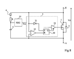
- Figure 8 partially represents elements of the circuit of FIGS. 4 and 6 according to a mode of preferred embodiment of the invention.
- Circuit 3 of Figure 8 includes the elements described in relation with FIG. only the controllable buffer 18 has been represented.
- the circuit 18 is controlled (enabled or disabled) to block the control signal of the transistor 1 under the effect of a flip-flop 30 of the RS type.
- the entrance 1 (S) of the flip-flop 30 is connected by an inverter 31, at the cathode K and its reset input (R) is connected to the output of an operational amplifier 32.
- Inverter inputs and non-inverting respective amplifier 32 are connected to K and A terminals.
- the role of such an assembly is to open the MOS transistor if, accidentally, the voltage at the terminals K and A reverses during a negative alternation. Indeed, as soon that the voltage Vd becomes positive, the output of the amplifier 22 switches to a high state, which blocks the amplifier 18. On the other hand, at each falling edge of the voltage Vd, the signal S goes to state 1, which activates amplifier 18.
- Figure 8 illustrates another variant concerning the supply circuit. This is to insert a resistance R between the diode 4 and the capacitor 5. This resistance R allows that the charging current of the capacitor 5 is of current type leakage while it is of the current type of recovery in the absence of resistance R. If necessary, the supplied voltage by the capacitor 5 can be regulated by a circuit 33 (REG) before supplying the voltage Vcc to block 3.
- REG circuit 33
- An advantage of the invention is that it allows have a unidirectional and autonomous rectification circuit likely to replace a diode in many applications.
- the invention makes it possible to replace a transistor in synchronous operation to the extent that the circuit makes an automatic synchronization with respect to the voltage present between terminals A and K.
- the invention makes it possible to preserve the position of the switch on the positive line (unlike the figure 2 where the transistor N1 is on the ground line). This avoids to cut the line of mass, which greatly improves the respect for electromagnetic constraints.
- Another advantage of the invention is that (with the exception short switching times (durations td2 and td1 + ter), the series voltage drop of the rectification element of the invention corresponds to that of a MOS transistor and is therefore considerably lower than that of a diode.
- connection of a recovery circuit according to the invention in a conventional converter is at the scope of the skilled person from the functional indications data above.
- MOS transistor is preferred, other switches are possible.
- bipolar transistor by providing a current control and oversizing capacity 5 power supply system.
Landscapes
- Engineering & Computer Science (AREA)
- Power Engineering (AREA)
- Dc-Dc Converters (AREA)
- Rectifiers (AREA)
Abstract
Description
Claims (11)
- Circuit de commande (3) d'un commutateur (1) à commander de façon unidirectionnelle alors que la tension présente à ses bornes est une tension alternative, caractérisé en ce qu'il comporte :des moyens pour retarder la fermeture du commutateur par rapport à un passage par zéro de la tension (Vd) à ses bornes ; etdes moyens pour déclencher l'ouverture du commutateur suite à sa fermeture, à l'issu d'un intervalle de temps prédéterminé (td1) majoré ou minoré d'un temps d'erreur (ter) asservi sur le rapport cyclique de la tension alternative aux bornes du commutateur, lors d'une ou plusieurs périodes précédentes.
- Circuit selon la revendication 1, dans lequel ladite durée prédéterminée (td1) est choisie en fonction des variations maximales attendues du rapport cyclique.
- Circuit selon la revendication 1, dans lequel un condensateur (5) et une diode (4) sont connectés en série entre les bornes (K, A) du commutateur (1) pour fournir une tension d'alimentation (Vcc) au circuit de commande (3), le condensateur étant chargé quand l'interrupteur (1) est ouvert.
- Circuit selon la revendication 1, comprenant :un circuit (R1, R2, 10) de détection du signe de la tension aux bornes du commutateur (1) ;un générateur de rampe (11, 12, 13, 14) réinitialisé à chaque changement de signe de la tension aux bornes du commutateur dans un sens où il doit devenir conducteur, ledit générateur étant commandé par le circuit de détection ;un moyen (15, 17, 18) pour provoquer la fermeture du commutateur suite à la détection d'un changement de signe de la tension à ses bornes ; etun circuit (15, 16, 19, 20) d'asservissement de la durée de fermeture sur une valeur prédéterminée.
- Circuit selon la revendication 4, dans lequel un premier élément retardateur (16) apporte un retard minimal (td1) à une consigne d'ouverture du commutateur (1) qui suit sa fermeture.
- Circuit selon la revendication 5, dans lequel un deuxième élément retardateur (17) apporte un retard à la fermeture du commutateur (1) par rapport à l'inversion de la tension à ses bornes.
- Circuit selon la revendication 1, dans lequel un amplificateur de sortie (18) fournissant le signal de commande du commutateur (1) est commandé par des moyens (30, 31, 32) de détection d'une inversion de sens de la tension, pour provoquer l'ouverture du commutateur en cas d'inversion accidentelle de tension.
- Circuit selon la revendication 1, dans lequel le commutateur est un transistor MOS.
- Circuit selon la revendication 1, dans lequel une diode en parallèle sur le commutateur sert au démarrage.
- Circuit de redressement à faible tension de seuil comprenant un commutateur (1) en parallèle avec une diode (2) constituée de préférence de sa diode parasite, et un circuit de commande (3) conforme à l'une quelconque des revendications 1 à 9, associé à un circuit d'alimentation (4, 5) prélevant son alimentation directement aux bornes du transistor commandé pendant que celui-ci est fermé.
- Circuit selon la revendication 10, comportant exclusivement deux bornes de connexion externe.
Applications Claiming Priority (2)
| Application Number | Priority Date | Filing Date | Title |
|---|---|---|---|
| FR0312816 | 2003-10-31 | ||
| FR0312816A FR2861916A1 (fr) | 2003-10-31 | 2003-10-31 | Commande d'un transistor mos en element de redressement |
Publications (2)
| Publication Number | Publication Date |
|---|---|
| EP1528661A1 true EP1528661A1 (fr) | 2005-05-04 |
| EP1528661B1 EP1528661B1 (fr) | 2008-07-09 |
Family
ID=34400894
Family Applications (1)
| Application Number | Title | Priority Date | Filing Date |
|---|---|---|---|
| EP04105379A Expired - Lifetime EP1528661B1 (fr) | 2003-10-31 | 2004-10-28 | Circuit de commande d'un transistor MOS pour redresseur synchrone |
Country Status (5)
| Country | Link |
|---|---|
| US (2) | US20050094424A1 (fr) |
| EP (1) | EP1528661B1 (fr) |
| JP (1) | JP2005137195A (fr) |
| DE (1) | DE602004014877D1 (fr) |
| FR (1) | FR2861916A1 (fr) |
Families Citing this family (12)
| Publication number | Priority date | Publication date | Assignee | Title |
|---|---|---|---|---|
| EP1722466A1 (fr) * | 2005-05-13 | 2006-11-15 | STMicroelectronics S.r.l. | Procédé et circuit correspondant pour générer une tension de commande d'un redresseur synchrone |
| CN100464486C (zh) * | 2006-04-30 | 2009-02-25 | 武汉万鹏科技有限公司 | 一种电源整流电路 |
| US8222874B2 (en) | 2007-06-26 | 2012-07-17 | Vishay-Siliconix | Current mode boost converter using slope compensation |
| DE102007060219A1 (de) * | 2007-12-14 | 2009-06-18 | Robert Bosch Gmbh | Gleichrichterschaltung |
| JP5817113B2 (ja) * | 2010-12-24 | 2015-11-18 | ソニー株式会社 | 音声信号出力装置、音声出力システム、音声信号出力方法 |
| JP6019553B2 (ja) | 2011-08-31 | 2016-11-02 | ソニー株式会社 | イヤホン装置 |
| JP5919686B2 (ja) | 2011-08-31 | 2016-05-18 | ソニー株式会社 | 音響再生装置 |
| CN102735914B (zh) * | 2012-05-10 | 2014-12-31 | 成都芯源系统有限公司 | 同步整流电路以及过零检测方法 |
| US9236809B2 (en) * | 2013-10-16 | 2016-01-12 | Texas Instruments Incorporated | Automatic timing adjustment for synchronous rectifier circuit |
| CN106130510B (zh) * | 2016-07-27 | 2023-04-07 | 山东省科学院自动化研究所 | 一种可调谐触发式超宽带窄脉冲产生装置及方法 |
| US10128736B1 (en) | 2017-06-23 | 2018-11-13 | Infineon Technologies Ag | Rectifier device |
| CN109149968B (zh) * | 2018-08-27 | 2020-07-28 | 重庆西南集成电路设计有限责任公司 | 一种同步整流二极管及同步整流控制电路 |
Citations (4)
| Publication number | Priority date | Publication date | Assignee | Title |
|---|---|---|---|---|
| US5268833A (en) * | 1991-05-14 | 1993-12-07 | U.S. Philips Corporation | Rectifier circuit including FETs of the same conductivity type |
| US5744994A (en) * | 1996-05-15 | 1998-04-28 | Siliconix Incorporated | Three-terminal power mosfet switch for use as synchronous rectifier or voltage clamp |
| EP0884829A1 (fr) * | 1997-06-11 | 1998-12-16 | International Rectifier Corporation | Convertisseur de passage monophasé avec un redressenent synchrone et un circuit de délai avec verrouillage de phase |
| EP0891038A1 (fr) * | 1996-11-13 | 1999-01-13 | Seiko Epson Corporation | Dispositif d'alimentation en energie et materiel electronique portatif |
Family Cites Families (6)
| Publication number | Priority date | Publication date | Assignee | Title |
|---|---|---|---|---|
| KR960016605B1 (ko) * | 1992-11-20 | 1996-12-16 | 마쯔시다 덴꼬 가부시끼가이샤 | 전원 공급 장치 |
| EP0723331B1 (fr) * | 1995-01-17 | 2003-05-07 | Vlt Corporation | Contrôle de l'énergie magnétique stockée dans les transformateurs des convertisseurs de puissance |
| US5781420A (en) * | 1996-07-18 | 1998-07-14 | International Power Devices, Inc. | Single ended forward DC-to-DC converter providing enhanced resetting for synchronous rectification |
| US6239994B1 (en) * | 1998-05-26 | 2001-05-29 | International Rectifier Corp | Secondary side switching regulator having a phase lock loop control circuit |
| US6768655B1 (en) * | 2003-02-03 | 2004-07-27 | System General Corp. | Discontinuous mode PFC controller having a power saving modulator and operation method thereof |
| US6839247B1 (en) * | 2003-07-10 | 2005-01-04 | System General Corp. | PFC-PWM controller having a power saving means |
-
2003
- 2003-10-31 FR FR0312816A patent/FR2861916A1/fr not_active Withdrawn
-
2004
- 2004-10-22 JP JP2004308057A patent/JP2005137195A/ja not_active Withdrawn
- 2004-10-28 EP EP04105379A patent/EP1528661B1/fr not_active Expired - Lifetime
- 2004-10-28 DE DE602004014877T patent/DE602004014877D1/de not_active Expired - Lifetime
- 2004-10-29 US US10/978,316 patent/US20050094424A1/en not_active Abandoned
-
2007
- 2007-09-20 US US11/903,192 patent/US7440299B2/en not_active Expired - Lifetime
Patent Citations (4)
| Publication number | Priority date | Publication date | Assignee | Title |
|---|---|---|---|---|
| US5268833A (en) * | 1991-05-14 | 1993-12-07 | U.S. Philips Corporation | Rectifier circuit including FETs of the same conductivity type |
| US5744994A (en) * | 1996-05-15 | 1998-04-28 | Siliconix Incorporated | Three-terminal power mosfet switch for use as synchronous rectifier or voltage clamp |
| EP0891038A1 (fr) * | 1996-11-13 | 1999-01-13 | Seiko Epson Corporation | Dispositif d'alimentation en energie et materiel electronique portatif |
| EP0884829A1 (fr) * | 1997-06-11 | 1998-12-16 | International Rectifier Corporation | Convertisseur de passage monophasé avec un redressenent synchrone et un circuit de délai avec verrouillage de phase |
Also Published As
| Publication number | Publication date |
|---|---|
| JP2005137195A (ja) | 2005-05-26 |
| US7440299B2 (en) | 2008-10-21 |
| FR2861916A1 (fr) | 2005-05-06 |
| US20080165556A1 (en) | 2008-07-10 |
| DE602004014877D1 (de) | 2008-08-21 |
| EP1528661B1 (fr) | 2008-07-09 |
| US20050094424A1 (en) | 2005-05-05 |
Similar Documents
| Publication | Publication Date | Title |
|---|---|---|
| EP1528661B1 (fr) | Circuit de commande d'un transistor MOS pour redresseur synchrone | |
| EP0722212B1 (fr) | Convertisseurs de tension bidirectionnels du type continu-continu et capteur de courant | |
| EP1334551A1 (fr) | Convertisseur de tension a circuit de commande autooscillant | |
| EP0002983A1 (fr) | Circuit de commande de puissance et alimentation à découpage l'utilisant | |
| EP0680245A2 (fr) | Ensemble comprenant un convertisseur statique à interrupteur commandé et un circuit de commande | |
| FR2596927A1 (fr) | Circuit de protection d'alimentation a decoupage | |
| EP0329571B1 (fr) | Dispositif de surveillance de démagnétisation pour alimentation à découpage à régulation primaire et secondaire | |
| EP3346597B1 (fr) | Convertisseur de puissance ac-dc | |
| FR2587155A1 (fr) | Circuit de commande pour des transistors mos de puissance a canal n montes dans des etages push-pull | |
| CA2723123A1 (fr) | Circuit de pre-charge pour convertisseur ac/dc | |
| EP1953904A1 (fr) | Circuit d'aide à la commutation pour un convertisseur à découpage | |
| EP1376843A2 (fr) | Commande d'un thyristor d'un pont redresseur | |
| EP1320919B1 (fr) | Limitation du mode continu d'un convertisseur de puissance | |
| EP1473818B1 (fr) | Circuit de commande d'un triac | |
| EP0265322B1 (fr) | Circuit de commande en mode veille d'une alimentation à découpage | |
| FR2662869A1 (fr) | Procede de limitation d'une surcharge base sur la technique de controle pwm (ou lc3) et dispositif electronique de mise en óoeuvre de ce procede. | |
| FR2778286A1 (fr) | Circuit convertisseur de tension | |
| EP3502826A1 (fr) | Circuit de recherche du point de puissance maximum | |
| EP0200600B1 (fr) | Circuit de commande de base de transistor fonctionnant à fréquence élevée | |
| EP2595279B1 (fr) | Dispositif d'alimentation à découpage et aéronef comprenant au moins un tel dispositif | |
| EP0176377B1 (fr) | Dispositif d'alimentation autonome pour dispositif d'observation, notamment à effet stéréoscopique | |
| EP0021867B1 (fr) | Dispositif d'alimentation à découpage régulé contre les variations de tension d'entrée et de puissance de sortie, notamment pour récepteur de télévision | |
| EP2781023A1 (fr) | Variateur de puissance | |
| FR2969864A1 (fr) | Circuit d'alimentation a faibles pertes en mode veille | |
| EP1493522A1 (fr) | Dispositif d'usinage par électroérosion |
Legal Events
| Date | Code | Title | Description |
|---|---|---|---|
| PUAI | Public reference made under article 153(3) epc to a published international application that has entered the european phase |
Free format text: ORIGINAL CODE: 0009012 |
|
| AK | Designated contracting states |
Kind code of ref document: A1 Designated state(s): AT BE BG CH CY CZ DE DK EE ES FI FR GB GR HU IE IT LI LU MC NL PL PT RO SE SI SK TR |
|
| AX | Request for extension of the european patent |
Extension state: AL HR LT LV MK |
|
| 17P | Request for examination filed |
Effective date: 20051103 |
|
| AKX | Designation fees paid |
Designated state(s): DE FR GB IT |
|
| GRAP | Despatch of communication of intention to grant a patent |
Free format text: ORIGINAL CODE: EPIDOSNIGR1 |
|
| GRAS | Grant fee paid |
Free format text: ORIGINAL CODE: EPIDOSNIGR3 |
|
| GRAA | (expected) grant |
Free format text: ORIGINAL CODE: 0009210 |
|
| AK | Designated contracting states |
Kind code of ref document: B1 Designated state(s): DE FR GB IT |
|
| REG | Reference to a national code |
Ref country code: GB Ref legal event code: FG4D Free format text: NOT ENGLISH |
|
| REF | Corresponds to: |
Ref document number: 602004014877 Country of ref document: DE Date of ref document: 20080821 Kind code of ref document: P |
|
| PLBE | No opposition filed within time limit |
Free format text: ORIGINAL CODE: 0009261 |
|
| STAA | Information on the status of an ep patent application or granted ep patent |
Free format text: STATUS: NO OPPOSITION FILED WITHIN TIME LIMIT |
|
| 26N | No opposition filed |
Effective date: 20090414 |
|
| PG25 | Lapsed in a contracting state [announced via postgrant information from national office to epo] |
Ref country code: IT Free format text: LAPSE BECAUSE OF FAILURE TO SUBMIT A TRANSLATION OF THE DESCRIPTION OR TO PAY THE FEE WITHIN THE PRESCRIBED TIME-LIMIT Effective date: 20080709 |
|
| PGFP | Annual fee paid to national office [announced via postgrant information from national office to epo] |
Ref country code: GB Payment date: 20110926 Year of fee payment: 8 |
|
| GBPC | Gb: european patent ceased through non-payment of renewal fee |
Effective date: 20121028 |
|
| PG25 | Lapsed in a contracting state [announced via postgrant information from national office to epo] |
Ref country code: GB Free format text: LAPSE BECAUSE OF NON-PAYMENT OF DUE FEES Effective date: 20121028 |
|
| PGFP | Annual fee paid to national office [announced via postgrant information from national office to epo] |
Ref country code: FR Payment date: 20131028 Year of fee payment: 10 |
|
| REG | Reference to a national code |
Ref country code: FR Ref legal event code: ST Effective date: 20150630 |
|
| PG25 | Lapsed in a contracting state [announced via postgrant information from national office to epo] |
Ref country code: FR Free format text: LAPSE BECAUSE OF NON-PAYMENT OF DUE FEES Effective date: 20141031 |
|
| PGFP | Annual fee paid to national office [announced via postgrant information from national office to epo] |
Ref country code: DE Payment date: 20230920 Year of fee payment: 20 |
|
| REG | Reference to a national code |
Ref country code: DE Ref legal event code: R071 Ref document number: 602004014877 Country of ref document: DE |